

Abstract
Due to its ultra-thin nature, the study of graphene quantum optoelectronics, like gate-dependent graphene Raman properties, is obscured by interactions with substrates and surroundings. For instance, the use of doped silicon with a capping thermal oxide layer limited the observation to low temperatures of a well-defined Kohn-anomaly behavior, related to the breakdown of the adiabatic Born–Oppenheimer approximation. Here, we design an optoelectronic device consisting of single-layer graphene electrically contacted with thin graphite leads, seated on an atomically flat hexagonal boron nitride substrate and gated with an ultra-thin gold layer. We show that this device is optically transparent, has no background optical peaks and photoluminescence from the device components, and no generation of laser-induced electrostatic doping (photodoping). This allows for room-temperature gate-dependent Raman spectroscopy effects that have only been observed at cryogenic temperatures so far, above all the Kohn-anomaly phonon energy normalization. The new device architecture, by decoupling graphene optoelectronic properties from the substrate effects, allows for observing quantum phenomena at room temperature.
Export citation and abstract BibTeX RIS
1. Introduction
Due to its two-dimensional nature and its electronic and optoelectronic properties, graphene is a promising material to be integrated into hybrid optoelectronic devices [1]. For instance, graphene/hexagonal boron nitride (hBN) heterostructure was used to confine light with small losses [2]. Besides, a 99.6% light absorption was presented using a device made of a polymethyl methacrylate grid, graphene, silica, and a gold layer [3]. A pursuit for alternative devices that detect and collect low-energy photons led Massicotte et al to make a heterostructure based on graphene  and hBN that converts low-energy photons into electricity through a photothermoelectric effect [4]. Graphene-based heterostructures were also applied in photoelectric modulators [5], photodetectors [6, 7], and light-emitting devices [8].
Two-dimensional field-effect transistors (2D-FETs) use gate voltages to probe electric field, charge carriers and quantum properties of 2D materials [9–16]. Especially, the combination of the non-destructive Raman technique, that probes the inelastic scattering of light, with graphene FETs unravels fascinating physics, like the Kohn-anomaly related to the breakdown of adiabatic Born–Oppenheimer approximation, electron-phonon coupling tuning and phonon softening [12, 14, 15]. However, the theoretically expected tendencies for gated-Raman measurements are not clearly observed at room temperature [12]. Fact that is attributed to temperature and charge inhomogeneity in graphene devices [12–15, 17]. Curiously, such problems were not solved after improvements in device quality, mainly achieved after incorporating hBN crystals on graphene field-effect devices [18], and the main reason is that transparent devices commonly show photodoping effects, which is the name attributed to changes on the density of free charge carriers in 2D FETs attained after light interaction [19–21]. Here, we present a device that decouples the graphene properties from its surroundings, allowing the observation of quantum properties at room temperature. The device shows transparency, no photodoping effects, and a clear and straightforward expected Raman dependency with gate-voltage. We observe the well-defined expected behavior due to the Kohn-anomaly, related to the breakdown of the adiabatic Born–Oppenheimer approximation, at room temperature. Such observations were only achieved because the graphene heterostructures are prepared by combining suitable transparent materials to avoid photodoping effects and background optical peaks; improvement that can be extrapolated to other 2D materials. Our work provides new insights into optoelectronic devices and allows the observation of quantum physics at room temperature with the proposed high-quality graphene device.
2. Device preparation
To implement field-effect graphene transistor for optoelectronics, graphene is deposited on one side of an insulating material, and another conducting material is placed on the other side to work as a gate electrode. From an optical perspective, several problems can occur: optical activity of any of the materials involved on the heterostructure can generate background or overlapping signals; the gate material is usually opaque, absorbing the optical-active peaks from graphene; interfaces between materials can be photo-active, impacting the field-effect performance, etc. Below, we describe a device that transcends these limitations.
Figure 1(a) shows a sketch of the device used in this work. We first pattern three thin (10 nm) gold (Au) leads by e-beam lithography, then we stack a heterostructure of graphite, graphene, and hBN (in this order) using the pick-up method and transfer it to the pre-patterned Au leads (see figure 1(a)). The Au leads were confectioned by e-beam lithography followed by thermal evaporation of 1 nm Cr sticking layer followed by the 10 nm Au layer on a coverslip (SiO2) substrate. We use the graphite to contact the graphene to the source (S) and drain (D) leads, while we use the gate (G) Au lead to apply a gate voltage ( ) to graphene. We use a confocal optical setup with backscattering illumination geometry (laser coming from the bellow). The laser wavelength is 632.8 nm and a laser power smaller than 1 mW to avoid laser damage. In most experiments, we focus our laser beam reaching a spotsize of 500 nm. Nonetheless, we defocused the laser in the measurements from figure 2 to ensure a large-area illumination. We prepared many devices of this kind, but in this manuscript, we present data of four, which we label Au1, Au2, Au3, and Au4. Au1 has a capping hBN layer, and the other devices are not encapsulated. We provide atomic force microscopy images of the gold layer that shows a uniform film, see figure S8. We use a thin 10 nm Au layer because of its transparency and absence of significant background reflection, being adequate for optical measurements. Notably, the heterostructure from figure 1(a) is expected to exhibit hybrid hyperbolic plasmon phonon-polaritons. However, we do not expect to observe any influence of this phenomenon in our results because it is active in the infra-red spectral region [22]. In contrast, our results are measured in the visible. Figure 1(b) shows an optical image of the device Au1. Figure 1(c) exhibits a Raman spectrum of this device, where we observe the hBN and the graphene C–C stretching G mode and the second-order breathing 2D mode Raman peaks. Although we measure a small background from the 10 nm thick Au layer, the graphene peaks are clearly observed, see figure 1(c). Hence, the device presented in figure 1 exhibits transparency and the absence of significant background optical peaks and luminescence. For completeness, we present investigations with devices using
  ,
,  , and
, and  gate electrodes, which do not show better results than the Au, see figures S1 and S2.
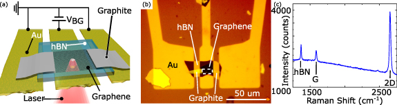
Figure 1. Device configuration. (a) Sketch of the device configuration. (b) Optical micrograph of the device. (c) Raman spectrum of the Au1 device.
Download figure:
Standard image High-resolution image
Figure 2. Photodoping generation in Au devices. (a) R vs  curves measured after laser exposures with the applied gate shown on legend. Exposure time of 2 min and laser power of 200 µW. (b) Photodoping model for the graphene–hBN–Au junction.
Download figure:
Standard image High-resolution image3. Absence of photodoping generation
Photodoping effects are typically observed when transistors made of 2D materials are exposed to light exposure [19–21, 23]. Although a photodoping effect permits applications on 2D photomemory devices [19], it is a critical problem for high-performance optoelectronic devices based on 2D-FETs. On a 2D-FET, the h-BN crystals work as insulators between the graphene and gate. Because hBN crystal has an energy gap of ∼5.9 eV [24], we do not expect any optoelectronic activity with the visible light. However, hBN loses its insulating property under interaction with visible light in some 2D-FETs. The reason is that the visible light photons excite the electronic states at the interface between hBN and the gate, breaking hBN insulating performance. Thus, the field-effect performance is affected, and charges are trapped in the heterostructure giving rise to photodoping [19].
So, photodoping hinders a proper investigation of the intrinsic properties of graphene, as well as its field-effect performance. For instance, [12] does not provide a data for G frequency and FWHM as a function of  that reveals clear Kohn-anomalies and electron–phonon coupling results. They use silicon with thermally grown SiO2 layer as substrate which is known to present photodoping [20, 23]. Figure 2(a) shows resistance (R) as a function of
  curves for the Au1 device to inspect its possible photodoping generation. For each curve, we keep
  at each potential and expose the device to the laser for 2 min. Then, we turn the laser off and repeat the R vs
  curve. This procedure was used to investigate photodoping, translated as shifts of the charge neutrality point (CNP) [19–21, 23]. During the measurements, we defocused our laser beam to increase the spotsize area and ensure we exposed to the laser a graphene region larger than 1 µm in accordance with [20, 23].
Because there are no CNP shifts for all exposures in figure 2(a), our device induces no photodoping in graphene. Thus, in such device the gate-voltage application does not compromise the measurement of graphene optoelectronic properties. We present in figure 2(b) the energy diagram of the graphene/hBN/Au junction as proposed in [19] to understand why our device has no photodoping. For negative gate voltages, photoexcited electrons from Au tend to flow towards graphene. However, this process only occurs if the laser energy ( ) is larger than the difference between Au work function (
 ) and hBN electron affinity (
 ). Thus, we expect metals with higher work functions to generate lower photodoping. Au work function is
  5.5 eV [25], which is the largest in this work, making Au a less photodoping gate material. Recall that the calculated work functions for WS2, MoS2 and WTe2 are approximately 4.5 eV, 4.75 eV 4 eV [26]. In figure 2(b),
  , while
  , points out the absence of photodoping generation in the proposed device. The reason to use a capping hBN on Au1 device in figure 2(b) measurement is to avoid laser-induced doping from air-contaminants. We also provide in figure S7 a leakage current test for Au1 device.
4. Room-temperature observation of well-defined Kohn-anomaly
To test the quality of the Au optoelectronic device, we analyze the frequency and full-width at half maximum (FWHM) of the G mode, see figures 3(a) and (b), and the frequency of the 2D mode (see figure 3(c)) as a function of Fermi-level for the Au2 device. We plot Fermi-level ( ) instead of
  to provide a better picture of the graphene's physical properties. Besides, we only plot the G FWHM and G and 2D frequencies in figure 3 because they have well-known physical mechanisms [12]. We evaluate the Fermi-level from the
  using the formula:

where  is the graphene's Fermi velocity [27],
  is the potential at graphene's charge neutrality point,
  is the hBN dielectric constant [28], and
  is the hBN thickness.

Figure 3. Raman feature properties as a function of the graphene Fermi level. (a) and (b) Frequency and FWHM as a function of Fermi energy for the G band, respectively. (c) Frequency as a function of Fermi level for the 2D band. This measurements are from the Au2 device.
Download figure:
Standard image High-resolution image
Figure 3(a) exhibits an expected modulation of the G frequency when changing  . Interestingly, for
  we observe two dips on the G frequency, which clearly show theoretically predicted details of the Kohn anomaly. The energy difference between these two dips is
  , as defined by the G phonon energy [29]. Figure 3(a) shows the raw data, with no treatment and no guide to the eyes nor modeling. Figure 3(b) shows a peak of G FHWM around 0 eV with a width of
  , again clearly delimitating the G phonon energy. For
  , G phonons cannot generate electron–hole pairs, increasing their lifetime and decreasing their energy linewidth [15] (approximately, since this is only absolute for T = 0 K). For completeness, figure 3(c) presents the 2D frequency vs
  . Here the Kohn-anomaly is not so well-defined, as expected, since the 2D peaks are related to phonons out of the high symmetry K-point, where the Kohn-anomaly is well marked. We provide similar data for the Au1, Au3, and Au4 devices in figures S3–S6. In total, we measured five datasets of gate-dependent Raman. Among them, four show a clear expected G frequency vs
  dependency due to the breakdown of the adiabatic approximation, with an 80% success rate. However, all the devices exhibit similar Raman features. Therefore, figure 3 provides unprecedented data with features that have only been experimentally observed so far at cryogenic temperature. Such clear data is achieved because the graphene FET is composed of suitable materials to be 'gateble' and photo-gating free.
5. Conclusion
In summary, we studied a high-quality graphene device made of hBN and a thin Au gate. We showed that this device allowed deep and clear data from the G Raman peak frequency and FWHM as a function of Fermi level. Accordingly, we observed the well-defined W-shaped Kohn-anomaly effects, related to the breakdown of adiabatic Born–Oppenheimer approximation, at room temperature. We attributed this achievement to our device aspects, which included transparency, absence of optical peaks close to G and 2D peaks, and lack of photodoping. Our work points toward the easier observation of graphene and other 2D materials intrinsic properties by using a high-quality and specific optoelectronic device.
6. Methods
6.1. Optical setup
We use a 632.8 nm radially polarized excitation laser focused by an oil-immersion objective (1.4 numerical aperture). We use laser power smaller than 1 mW to avoid damage to the heterostructure. The back-scattered light is collected by a spectrometer equipped with a charge-coupled device. We focus our laser on reaching a 500 nm spot size for the gate-dependent Raman experiments. For the photodoping measurements, we defocus the laser, reaching spot sizes larger than 1 µm.
6.2. Sample preparation
To prepare the Au devices, we first do e-beam lithography on a coverslip substrate. Then, we thermally evaporate 1 nm Cr sticking layer followed by the 10 nm Au layer. Next, we do a lift-off in acetone bath at 80 ∘C for 20 min and rinse in isopropanol and N2 blow-dry. Next, we use the pick-up method described in [30] to stack the heterostructure and transfer it to the pre-patterned coverslip substrate. The hBN and graphite thicknesses are typically 30 nm and 20 nm, respectively. For the heterostructures that use TMDs as the gate, their thickness is 20–30 nm.
Acknowledgments
This work was supported by CNPq (302775/2018-8, 436381/2018-4, 305881/2019-1, and INCT/Nanomaterials de Carbono), Finep (SibratecNano 21040), CAPES (RELAII and 88881.198744/2018-01) and FAPEMIG, Brazil. A C G and M B R acknowledge partial support from DoE Award No. DE-SC0008807.
Data availability statement
The data that support the findings of this study are available upon reasonable request from the authors. The experimental data related to this work can be obtained upon request to the contact authors.
Authors contribution
Sample preparation: Andreij C Gadelha and Tiago C Barbosa. Raman measurements: Andreij C Gadelha and Rafael Nadas. Data Analysis: Andreij C Gadelha, Rafael Nadas and Ado Jorio. Project idealization and guidance: Ado Jorio, Andreij C Gadelha, Leonardo C Campos and Markus B Raschke. Paper writing: Ado Jorio, Andreij C Gadelha and Rafael Nadas.
Conflict of interest
The authors declare no competing financial interests.
Supplementary data (4.4 MB PDF)