
Abstract
The doping of quasi-freestanding graphene (QFG) on H-terminated, Si-face 6H-, 4H-, and 3C-SiC is studied by angle-resolved photoelectron spectroscopy close to the Dirac point. Using semi-insulating as well as n-type doped substrates we shed light on the contributions to the charge carrier density in QFG caused by (i) the spontaneous polarization of the substrate, and (ii) the band alignment between the substrate and the graphene layer. In this way we provide quantitative support for the previously suggested model of polarization doping of graphene on SiC (Ristein et al 2012 Phys. Rev. Lett. 108 246104).
Export citation and abstract BibTeX RIS
1. Introduction
Silicon carbide (SiC) crystals have evolved as the substrates of choice for graphene growth [1–3]. Epitaxial graphene (EG) on SiC has been a subject of intensive research due to various promising applications, such as, e.g., high frequency transistors [4–6], frequency mixers [7] or resistance standards [8]. The process of precisely controlling the number of graphene layers [2] and the determination of the basic parameters of the band structure and its dependence on the number of layers [10] or on interface modification is of great importance for the future of carbon-based nanoelectronics. Although different polytypes such as 3C-, 4H- and 6H-SiC are available, such fundamental questions as how the charge carrier concentration and type in the graphene layers varies with the substrate polytype and substrate doping remain largely unanswered. This issue plays a very important role in the research of graphene on SiC, as well as in its industrial applications. In this study we experimentally address this issue and create a rational basis for the choice of substrate for future graphene-on-SiC applications.
It is well known that EG on SiC(0001), which is situated on top of the so-called buffer layer (denoted by  in the figures of this work) is intrinsically n-type doped [1, 9, 10]. Note that the buffer layer is already a honeycomb lattice of carbon atoms, but on account of hybridization with SiC states it does not exhibit the Dirac-like dispersion at the K-point of the Brillouin zone [9, 11–13]. A model by Kopylov et al [14] explained the n-type doping by either bulk or interface donor states.
The situation changes when going from EG on the buffer layer to quasi-freestanding graphene (QFG) on H-terminated SiC(0001) [15–20]. The latter is obtained—as was first shown by Riedl et al [15, 16]—by annealing the buffer layer in an atmosphere of hydrogen. Hydrogen intercalates between the SiC surface and the buffer layer, saturating the dangling bonds of the topmost Si atoms [21, 22]. In that way, the buffer layer is decoupled from the SiC surface. On account of the dramatically reduced interaction of the now H-terminated SiC(0001) surface with the carbon atoms, an almost undisturbed graphene layer emerges which is referred to as QFG. For details about the preparation see also section 2. In contrast to EG, QFG has an excess of holes. This p-type doping cannot be explained by the model of Kopylov [14]. Instead, it has been attributed to the influence of the spontaneous polarization of the hexagonal SiC substrate [23].
The spontaneous polarization (which is a bulk property) leads to a polarization charge on the polar surfaces of hexagonal semiconductor compounds, such as SiC and GaN, which is usually compensated by internal charge formation due to depletion/accumulation of charge carriers or by external buildup of ionic charge on the surfaces. Only the modulation of the polarization charge at a surface upon an external perturbation can be measured [24–26], making the effect itself difficult to address experimentally. The existence of various SiC polytypes offers an excellent opportunity to address the question. While spontaneous polarization is absent for the cubic polytype 3C-SiC due to symmetry, it is mainly induced at the inversion of the stacking sequence of the SiC double layers in the hexagonal polytypes. Consequently, varying the hexagonality of the SiC polytype changes the polarization proportionally. Thus, for 4H-SiC(0001) it is expected to be  times larger than for 6H-SiC(0001) [27–30].
In order to test this hypothesis, we have carried out systematic angle-resolved photoelectron spectroscopy (ARPES) measurements close to the Dirac point. In particular, the comparison of the total charge densities of QFG on 6H-SiC(0001), 4H-SiC(0001) and 3C-SiC(111) provides a quantitative confirmation of the polarization doping proposed earlier [23]. In addition, by comparing n-type and semi-insulating substrates with identical graphene layers on top we provide further additional insights into the question how the charge carrier density in graphene overlayers is influenced by the doping level of the SiC bulk.
2. Sample preparation and characterization
EG was formed by sublimation growth in argon atmosphere [2] on the Si-face of various SiC substrates. Nitrogen doped n-type 6H-SiC(0001) was purchased from SiCrystal AG while semi-insulating 6H-SiC wafers were obtained from II–VI Inc. Semi-insulating (SI) as well as N-doped, n-type 4H-SiC wafers were purchased from Cree Inc. Finally, a sample of 3C-SiC with (111) surface orientation grown on a 6H-SiC(0001) substrate was prepared at Linköping University. Growth of EG (including samples covered by the buffer layer only) was performed using a custom built reactor which is described elsewhere [31]. By adjusting the temperature and the Ar pressure, the thickness of EG can be controlled from the pure buffer layer ( ) to up to three monolayers on the buffer layer. The different EG samples are denoted as MLG, BLG, and TLG for one, two, or three layers of graphene on top of the buffer layer, respectively. Growth parameters are summarized in table 1.
Table 1.
Parameters (annealing temperature T, argon pressure pAr, Ar flow rate  , hydrogen pressure
  , hydrogen flow rate
  , and annealing time t) used for the preparation of the samples. Note that parameters vary between different growth setups so that the values given here cannot be transferred directly to other equipment.
| Growth of EG | ||||
|---|---|---|---|---|
| Sample | T(°C) | pAr/mbar |
 /slm /slm |
t/min |

|
1450 | 1000 | 0.1 | 15 |
| MLG | 1650 | 1000 | 0.1 | 15 |
| BLG | 1750 | 400 | 0.1 | 15 |
| TLGa | 1800 | 400 | 0.1 | 15 |
| Intercalation | ||||
| Sample | T(°C) | pH2/mbar | ϕH2/slm | t/min |
| QFMLG | 540 | 900 | 0.9 | 90 |
| QFBLG | 840 | 900 | 0.9 | 90 |
| QFTLG | 880 | 900 | 0.9 | 120 |

QFG was prepared by annealing in ultra-pure hydrogen [15–18] using a custom built setup and parameters also listed in table 1. As mentioned above, hydrogen saturates the SiC surface, thereby releasing the buffer layer. Hence, carrying out H-intercalation with a sample that consists only of the buffer layer, quasi-freestanding monolayer graphene (QFMLG) is obtained. In the same way, MLG and BLG are converted into quasi-freestanding bilayer graphene (QFBLG) and quasi-freestanding trilayer graphene (QFTLG), respectively. In other words, the conversion of the buffer layer adds one graphene layer to the stack. Note that this process is not hydrogenation of graphene, as only the SiC substrate surface is saturated with hydrogen.
Following preparation the samples were characterized by photoelectron spectroscopy. X-ray induced photoelectron spectroscopy (XPS) was carried out using a SPECS PHOIBOS 150 MCD 9 analyzer in conjunction with a monochromatized Al  source (SPECS FOCUS 500). ARPES spectra were collected with the help of a SPECS PHOIBOS 100 2D CCD system operated at beam line UE56/2-PGM1 of the synchrotron radiation source BESSY II. All measurements were carried out at a pressure of
  mbar or lower. While XPS was performed at room temperature, the ARPES data was collected with the sample held at a temperature of 80 K. Prior to the measurements, the ex situ prepared samples were carefully annealed at 350°C to remove possible contaminations from exposure to air. Note that a comparative study like the present one can only be carried out when identical preparation techniques and analytical tools are used.
3. Results and discussion
3.1. XPS analysis
The process of conversion of EG films to QFG layers is illustrated in figure 1 by a series of XPS spectra. The C1s core-level spectra shown in that figure are comprised of various components, which can be attributed to C atoms in the SiC substrate ('SiC'), the buffer layer ('S1' and 'S2' [9]), and the graphene layer ('graphene'). It is clear from figure 1 that in all three cases components S1 and S2 vanish after H-intercalation, which confirms the transformation from epitaxial graphene to QFG. The shift of the SiC signal upon H-intercalation is caused by a different surface band bending which will be commented on later. Most importantly, the position of the graphene component also differs depending on the interface. For EG on the buffer layer, the position is at a higher binding energy than for QFG. In fact, the C1s core line of graphene indicates already a change from n-type doping for EG to p-type doping for QFG, as already observed before [15–18]. The experimental uncertainty of the XPS core level spectra (approximately  eV) is, however, too large to perform a more precise analysis of the charge carrier concentration. This will be done with the help of the ARPES measurements described in the next section.
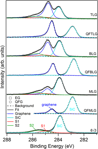
Figure 1. C1s core-level spectra of graphene on 6H-SiC(0001) before ( , MLG, BLG) and after H-intercalation (QFMLG, QFBLG, QFTLG). Each spectrum is analyzed in terms of components arising from the SiC substrate ('SiC'), the graphene ('graphene'), and (where applicable) from the two buffer layer components ('S1', 'S2'). In addition, the spectrum of trilayer graphene (TLG) is also shown for comparison.
Download figure:
Standard image High-resolution image3.2. ARPES
Figure 2 shows ARPES measurements of QFG on n-type (bulk carrier concentration of  ) and semi-insulating (bulk carrier concentration of less than
  ) 6H-SiC(0001) (a)–(d) and 4H-SiC(0001) (e)–(h) substrates. As expected, the number of π-bands increases from one for QFMLG to two for QFBLG. It is obvious that the Dirac point (
 ) is located above the Fermi energy (
 ) for all hexagonal substrates. In order to learn more about the position of
  , the observed bands were fitted with a tight binding model as already used in earlier work [10]. The Fermi velocity turns out to be
  and the interlayer hopping matrix element, which is important for bilayers, is
  eV, in agreement with previous work [10]. The position of the bands observed for QFBLG indicates the presence of a small band gap due to an asymmetry
  in the onsite Coulomb potentials
  on the two layers [32, 33]. The band gap is above
  and therefore not directly visible in ARPES. However, recent two-photon photoemission (2PPE) experiments [34] have given direct evidence for its existence. The fitting parameters are collected in table 2.

Figure 2. π-bands near  for QFMLG and QFBLG on (a), (b) n-type 6H-SiC(0001), (c), (d) semi-insulating 6H-SiC(0001), (e), (f) n-type 4H-SiC(0001), (g), (h) semi-insulating 4H-SiC(0001) and (i) n-type 3C-SiC(111). The photon energy was
  eV. The blue lines show fitted tight binding bands. The insets depict the corresponding Fermi surfaces. Schematic representation of graphene in reciprocal space on the right shows directions of kx and ky vectors.
Download figure:
Standard image High-resolution imageTable 2.
Properties of QFG on the different SiC substrates.  is the position of the Dirac point with respect to
  determined by fitting a tight-binding model to the ARPES data.
  is the difference in the onsite Coulomb potentials and γ the interlayer coupling constant of the QFBLG samples. p is the hole concentration. Its value is given per unit cell and per
  .
.
| Sample |
 /eV /eV |
 /eV /eV |
γ/eV | p/unit cell | p/ |
|---|---|---|---|---|---|
| QFMLG/6H-n | 0.24 |

|

|
||
| QFBLG/6H-n | 0.14 | 0.12 | 0.38 |

|

|
| QFMLG/6H-SI | 0.28 |

|

|
||
| QFBLG/6H-SI | 0.22 | 0.12 | 0.38 |

|

|
| QFMLG/4H-n | 0.30 |

|

|
||
| QFBLG/4H-n | 0.22 | 0.12 | 0.38 |

|

|
| QFMLG/4H-SI | 0.34 |

|

|
||
| QFBLG/4H-SI | 0.28 | 0.12 | 0.40 |

|

|
| QFMLG/3C−n | −0.1 |

|

|
The hole density p (per unit cell) was determined from the π-band Fermi surface area  from figure 2 using the simple relationship

where  is the area of the first Brillouin zone of graphene and coefficient gs = 2 due to the spin degeneracy. It is worth noting that a part of the photoemission intensity at the Fermi surface is suppressed by the 'dark corridor' effect due to the influence of the pseudospin [35, 36]. Fermi surfaces were approximated by circles. The total charge carrier concentration calculated from the Dirac point position from the fit was consistent with that extracted from the Fermi surface area as shown in table 2. Note that the charge density hardly changes with the thickness of the graphene stack, in agreement with the behavior observed with EG on SiC(0001) [10]. From figure 2 the reason for this becomes immediately obvious: even for multilayer QFG (shown here only QFBLG) only the uppermost of the π-bands is emptied of electrons, i.e. involved in the doping process by equilibrating with the (pyroelectric!) substrate. The additional π-bands are far enough below the Fermi level to be completely occupied. This clarifies how the position of
  changes with the addition of graphene layers on SiC. It becomes lower in order to adjust to the hole concentration values of
  and
and  for QFG on semi-insulating 4H-SiC(0001) and 6H-SiC(0001), respectively.
The doping level of QFG does, however, depend on the polytype of the substrate. For QFMLG layers on semi-insulating 4H-SiC(0001) the hole concentration extracted from the Fermi surface measurement is  , in comparison to
  for QFMLG layers on semi-insulating 6H-SiC(0001) with the same bulk doping level. This is in very good agreement with the spontaneous polarization doping model [23] which predicts that the doping should be 1.5 times larger for QFMLG on 4H-SiC(0001) than for QFMLG on 6H-SiC(0001) due to the larger polarization of the substrate [27–30]. This observation strongly corroborates the polarization doping model. We note in passing that this model was also corroborated by a previous report of mild n-type doping of
  for QFMLG on 3C-SiC(111) [37], which is confirmed by our measurement in figure 2(i), where we get a n-doping of
  . This mild n-type doping on cubic substrates is explained by substrate bulk doping below.
Finally we would like to address the influence of the substrate bulk doping level on the hole concentration in QFG layers on top. For QFG on both 6H-SiC and 4H-SiC polytypes, doping was observed to be systematically lower for n-type than for semi-insulating substrates. This effect can be explained by a depletion layer areal charge density in the SiC. In the spirit of the polarization doping model [23], the negative pseudo polarization charge—which is a fixed number characteristic for the polytype of the SiC substrate—is balanced by the holes in the QFG layers and a positive space charge in the substrate depletion layer. For the latter one, the areal charge density  is given by

where  is the vacuum permittivity,
  the dielectric constant of SiC,
  the SiC doping concentration, and
  the surface band bending of the substrate. The latter can be extracted [38, 39] from the XPS core level measurements shown in figure 1. The band alignment between the substrate and graphene for QFMLG on 4H- and 6H-SiC substrates with different bulk donor doping is shown in figure 3. It is worth noting that band bending is almost invariant with addition of extra layers, thus calculations below are true for multilayer systems as well.

Figure 3. Band diagrams of QFMLG on SiC(0001). (a) n-type 6H-SiC, (b) semi-insulating 6H-SiC, (c) n-type 4H-SiC, and (d) semi-insulating 6H-SiC. The bulk doping concentration of the n-type and semi-insulating substrates are  and
and  , respectively. Note that the accuracy of the core level binding energies (approximately
  eV) is worse than that of the ARPES measurements (about
  eV).
eV).
Download figure:
Standard image High-resolution image
By substituting the parameters into equation (2) one obtains  for QFG on n-type 6H-SiC(0001) with
  and
and  for semi-insulating 6H-SiC with
  . Using the same formula we obtain
  for QFG on n-type 4H-SiC(0001) with
  and
and  for semi-insulating 4H-SiC with
  . One should note that the number for bulk carrier concentration contains a rather large uncertainty (
 for n-type samples). Whereas
  is negligible for the semi-insulating substrates, its magnitude for the n-type case is within the uncertainty we have conceded consistent with the difference of around
  in the areal hole density of semi-insulating and n-type SiC substrates (see last column in table 1). The electron transfer due to the depletion of the n-type 3C-SiC substrate also naturally explains the n-type doping of the QFMLG layer on that substrate.
4. Conclusions
Multilayer EG and QFG on the Si-face of three different polytypes of SiC was investigated by XPS and ARPES. The hole concentration was observed to depend in a characteristic manner on the SiC polytype as predicted by the polarization doping model [23]. 4H-SiC, which has the largest spontaneous polarization, induces the largest carrier concentration in QFG, followed by 6H-SiC whose polarization and induced hole concentration are approximately 1.5 times smaller. 3C-SiC, which has no spontaneous polarization, induces a negligible n-type doping in QFG which is presumably due to bulk doping, i.e. the depletion of the n-type SiC substrate. The experiments provide strong evidence in favor of the polarization doping model [23]. The model also provides a roadmap for the choice of substrates for QFG. Clearly, 3C-SiC would be the substrate material of choice because it allows the lowest charge carrier concentration. On the other hand it was shown previously that the deposition parameters for the growth of dielectrics can be tuned to vary surface transfer doping of graphene [40]. This together with the polytype-dependent polarization doping could provide a basis for tuning the charge carrier concentration in QFG on hexagonal SiC polytypes.
The effect of polarization doping as well as bulk doping on graphene overlayers naturally takes place not only for QFG, but also for EG on SiC. In that case, the magnitude of this effect is apparently overcompensated by charge transfer from interface states such as, e.g., dangling bonds.
Finally it is worth noting that polarization doping should also be considered for graphene and other 2D materials on pyroelectric substrates. In conjunction with piezoelectric substrates, where the polarization is changed by external forces, this effect could lead to novel applications in electronic devices.
Acknowledgments
The authors are grateful to Karsten Horn, Hendrik Vita and Stefan Böttcher from the Fritz-Haber-Institute for their ongoing support during beam times at BESSY II as well as for fruitful discussions. The research leading to these results has received funding from the European Union Seventh Framework Programme under grant agreement n°604391 Graphene Flagship, from the DFG within the Collaborative Research Centre SFB 953 Synthetic Carbon Allotropes and within the Priority Programme SPP 1459 Graphene (SE 1087/10-1), as well as from the European Science Foundation under the EUROCORES Programme EuroGraphene (SE 1087/9-1).