


Abstract
Resistive switching (RS) is studied in a memristor based on a ZrO2(Y)/Ta2O5 stack under a white Gaussian noise voltage signal. We have found that the memristor switches between the low resistance state and the high resistance state in a random telegraphic signal (RTS) mode. The effective potential profile of the memristor shows from two to three local minima and depends on the input noise parameters and the memristor operation. These observations indicate the multiplicative character of the noise on the dynamical behavior of the memristor, that is the noise perceived by the memristor depends on the state of the system and its electrical properties are influenced by the noise signal. The detected effects manifest the fundamental intrinsic properties of the memristor as a multistable nonlinear system.
Export citation and abstract BibTeX RIS
1. Introduction
In recent years, the investigations of resistive switching (RS) have attracted a lot of attention [1]. The effect of RS consists of the bistable, or multistable, switching of the resistance of thin dielectric films inserted between two conductive electrodes under the external voltage applied between the electrodes [2]. The thickness of the films ranges from several nanometers to several tens nanometers. Within the context of nanotechnologies, production of nanostructures by diffusion is a subject largely investigated [3–5]. The electronic devices, whose operation is based on RS, are called memristors [6]. Memristors are considered promising for application in the next non-volatile generation computer memory, that is resistive random access memory (ReRAM) [7], in the neuromorphic computer systems [8], etc.
The current understanding of the RS mechanism in metal oxides is based on the concept of formation of conductive filaments constituted by the diffusion of the oxygen vacancies between the conductive electrodes in the electric field between the electrodes (shortcutting these ones) in so-called forming process [9]. Switching of a memristor from the low resistance state (LRS) to the high resistance state (HRS) is obtained from the rupture of the filament by a voltage pulse, the so-called reset process. The filament can be restored by a voltage pulse of the opposite polarity that causes the transition from HRS to LRS, the so-called set process. The phenomena described above constitute a physical basis of the so-called bipolar RS.
It should be emphasized here that the RS is essentially a random process. The typical size of the filament cross section is in the range of 1–10 nm [10]. Usually, the rupture and the restoration of the filaments in the oxides takes place near the filament interface with one of the electrodes, through the jumps of the O2 − ions through the oxygen vacancies in a small volume, several cubic nanometers, near the filament tip. A very limited (countable) number of O2 − ions (or oxygen vacancies) is involved in RS [11]. So far, a memristor appears to be essentially a mesoscopic system. The dispersion and natural randomness of the parameters of the memristor, which is a fundamental property of the RS, currently limits the application of the memristor [12].
The memristor can be treated as a nonlinear bistable system, in the simplest case, or multistable. It should be noted that the coexistence of different stable states for a given set of parameters has been observed in many natural and experimental systems in various fields such as laser and semiconductor physics, chemistry, ecology, neuroscience, and climate dynamics (see the review [13] and references therein). Multistable systems are characterized by a high degree of complexity in their behavior due to the 'interaction' between attractors. Moreover such systems can be described with the methods of statistical physics. In particular, in such systems, a well-known phenomenon, that is stochastic resonance [14–17] can occur, in which noise plays a constructive role [18–23]. Indeed, there are many known examples in classical and quantum physics, where the interplay between noise and nonlinearity can give rise to counterintuitive dynamical behaviors [24–34]. In particular, in [35] the authors analyzed theoretically how the average state of a resistor could be changed by simply applying white noise, in [33] it was shown that internal noise helps increase the contrast ratio between low and high resistance states, and in [34] a phenomenon similar to stochastic resonance was experimentally observed, showing the beneficial role of noise in resistive switching. The authors of [34] interpreted their results in terms of stochastic resonance. However, it is still unclear whether the statistical physics approach is applicable to the description of the memristor. In particular, it is not clear how many local minima are in the memristor's potential profile. Therefore, Karpov with co-workers [36] proposed the conductive transformation of the filament in the memristors through nucleation and growth stages, similar to standard phase transitions, and assumed that a nucleation could evolve in two steps, through an intermediate metastable state. Indeed, metastability and nonequilibrium steady states are very general features in the physics of complex systems [37–39].
As a result, two thermodynamics barriers separating two stable states and a metastable state appear in some configuration spaces. A possibility of tristability in memristor behavior has also been discussed in [40]. A conceptual solution has been suggested for a three-state adder based on tristable memristive devices to take advantage of the multi-bit storage capabilities of the memristor for digital arithmetic circuits.
In this paper, we experimentally analyze the response of a memristor based on a ZrO2(Y)/Ta2O5 stack into a white Gaussian noise signal. The bilayer ZrO2(Y)/Ta2O5 stack-based memristors have been selected as sample objects for experimental studies because of the longer duration of such memristors [41]. The objective of the present work is the search for the fundamental phenomena that characterize the memristor as a complex nonlinear multistable system. We have observed a random switching of the memristor between the HRS and LRS, as in the random telegraph signal (RTS), under an external Gaussian white noise voltage signal. The potential profiles of memristors extracted from their response to Gaussian white noise signal show from two to three local minima. Moreover, these potential profiles depend on the input noise parameters and, of course, on the time because of the transient dynamics of the memristors. These observations indicate the multiplicative character of the impact of noise on the memristor, that is the noise perceived by the system depends on the state of the memristor and its electrical properties are influenced by the noise signal. Moreover these properties together with the noise change during the memristor aging. These observations manifest the fundamental intrinsic properties of the memristor as a multistable nonlinear stochastic system.
The paper is organized as follows. In section 2, the details of the preparation of the sample memristor are described, as well as the experimental techniques to analyze the memristor response to an external white Gaussian noise. In section 3, the experimental results are presented and discussed. The conclusions section summarizes the results of the present study.
2. Experimental setup
The memristors investigated in the present study are fabricated from the ZrO2(Y)/Ta2O5 thin-film stacks (each layer is  10 nm in thickness) formed by radio-frequency magnetron sputtering using Torr International® 2G1-1G2-EB4-TH1 vacuum setup for thin film deposition. Standard factory-made Si(0 0 1) substrates are used with pre-deposited SiO2 layers (500 nm in thickness), the adhesion Ti layers and the conductive TiN ones (each 25 nm thick). The substrate temperature when depositing the functional dielectric stacks is 300 °C, the pressure of Ar–O2 (50:50% mol.) gas mixture inside the deposition chamber is ∼10−2 Torr. The molar fraction of the stabilizing oxide Y2O3 in the pressed powder ZrO2(Y) target material is
  0.12.
0.12.
After the deposition of the ZrO2(Y) layers, the 8 nm thick Ta adhesion layers and the contact 20 nm thick Au ones are deposited by direct current magnetron sputtering at 200 °C. From these stacks, the cross-point memristors are fabricated by standard optical photolithography with wet chemical etching. The lateral sizes of the active area of the memristors are 
 m2. Finally, the devices are packaged into standard closed metal/ceramic integrated circuit packages. More details on the memristor fabrication procedure as well as on the characterization of their electrical parameters can be found in [41]. The forming and preliminary electrical characterization of the memristors are performed using Agilent® 1500A semiconductor device analyzer. The cyclic current–voltage (I–
 ) curves of the memristor are measured by sweeping the ramp voltage
  from
from  up to
up to  and back down to
  and so forth. The compliance of the current, when forming and measuring the cyclic I–
 curves, is set to 300
  A.
A.
The response of the memristors to the noise signal is investigated using a home-made setup shown schematically in figure 1. The bias voltage  applied to the memristor is supplied by the digital-to-analog converter (DAC) of National Instruments® TnUSB 6211 computer-controlled DAC/ADC unit operated as a programmable voltage source under LabView® 2016 software. The output voltage range of the DAC is
  10 V, the maximum output bitrate is 250 kHz. The voltage from the DAC output is then amplified up to the maximum magnitude 25 V by a wide bandpass dc operation voltage amplifier. The bandpass of the amplifier is 0 to 2 MHz. The output signal is taken from the load resistor Rn = 1 k
 and is supplied to the analog-to-digital converter (ADC) of the National Instruments® TnUSB 6211 DAC/ADC unit. The maximum sampling rate of the ADC is 250 kHz. The output signal waveform is monitored by Agilent® 3000A digital oscilloscope.
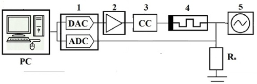
Figure 1. Schematic representation of the experimental setup. 1—DAC/ADC unit, 2—amplifier, 3—current compliance, 4—memristor, 5—oscilloscope,  —load resistor.
Download figure:
Standard image High-resolution imageFirst, several cyclic I– curves of the memristor are measured in order to ensure the RS. The I–
 curves are measured with the current compliance of 300
  A provided by a field effect transistor (FET) shunted by a diode. Afterwards, the compliance of the current unit is switched off, and the artificial noise signal
  with the predefined magnitude is supplied directly to the memristor. The external noise signal is generated using a random number generator ADSViewer-2 (v.015) [42] and is saved in a control computer. The noise data array contains up to 106 random numbers. Before measurements, noise data are read into the random access memory (RAM) of the control computer. The magnitude of the noise signal is characterized by the output voltage standard deviation
  . Finally, a constant offset voltage
  is added to the noise data. The resulting noise signal is played back, sent to the DAC of the DAC/ADC unit, in an endless cycle with predefined bit rate equal to the maximum bit rate provided by the DAC, with 250 000 numbers per second that corresponds to the white noise spectrum bandwidth from 0 to 250 kHz. In the experiment, the waveforms of the current flowing through the memristor
  are measured subject to the noise signal parameters
  and
and  .
.
3. Results and discussion
In figure 2 the typical cyclic I– curve of the investigated memristors is shown, including the forming process and several hysteresis loops, typical for bipolar RS. Due to the asymmetry of the memristor structure, different values of
  V and
V and  V are measured.

Figure 2. Typical I– curve of a memristor based on the ZrO2(Y)/Ta2O5 stack.
Download figure:
Standard image High-resolution imageThree typical waveforms  and respective distribution histograms of I, under the external noise signal
  with
with  with different values of the noise intensity
  , are shown in figure 3. For some parameters of the noise signal, the memristor switches between the HRS and the LRS as a random telegraph signal (RTS) (see figure 3(b)). This behavior is typical for bistable or even multistable systems in a heat bath. The experimental results obtained in the present study aim to the applicability of the formalism used in statistical physics to describe the impact of noise on nonlinear multistable systems for understanding the stochastic resistive switching of memristors.
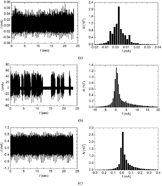
Figure 3. Typical waveforms (left) and related distribution histograms (right) of the current I flowing through the memristor under the noise signal.  V.
V.  , V: 0.4 (a), 0.75 (b), 1.2 (c).
Download figure:
Standard image High-resolution imageIn the following figure 4 is shown the plot of the parameter space,  , in which the resistive switching is observed (black triangles) or not observed (white circles). Specifically, the experiments, in which the RS of the memristor under the noise signal is observed, are marked by black triangles. These points define a field in the space of the experiment parameters, inside which the noise-induced RS of the memristor takes place. Note that the noise-induced RS is observed at two different values of
  , namely 0.2 and 0.5 V, due to the asymmetry of the cyclic I–
 curves of the memristor (see figure 2). Outside this field, the memristor acts as nonlinear resistor being either in the HRS (see figure 3(a)) or in the LRS (figure 3(c)). Accordingly, the respective distribution histograms of I deviates form the Gaussian one, inherent to the input noise signal (see the right panels of figure 3).
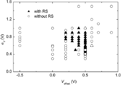
Figure 4. The plot of the parameter space of the experiment:  , in which the resistive switching is observed (black triangles) or not observed (white circles).
Download figure:
Standard image High-resolution imageIn order to analyze the distribution of the current I in the noise-induced RS regime, let us consider a cyclic I– curve of an ideal memristor presented in figure 5(a). In the ideal case, the branches corresponding to the HRS and LRS are represented by linear functions with different slopes, in other words the memristor is considered as a two-position linear switch. Let us assume a random voltage
  with Gaussian distribution applied to the memristor. In the HRS, the probability distribution of the current I through the memristor will also be Gaussian. In the LRS, the probability distribution of I will be Gaussian too, but the width will be greater than in the HRS. If the memristor switches between the HRS and LRS many times within a period of observation T long enough with respect to the average lifetime
  of the memristor in HRS (LRS), that is
  , the resulting probability distribution of I should be a superposition of two Gaussian functions with related widths. Indeed, the experimental histogram of the probability distribution of I in the noise-induced RS regime can be approximated by a superposition of two Gaussian functions as shown in figure 5(c), where the distribution histograms of the current flowing through a memristor I in the noise-induced RS mode (
 V;
V;  V), for LRS (red curve), HRS (blue curve) and superposition of the previous curves (purple curve) are shown. In the case when a non-zero bias
  is added to the Gaussian noise signal, the centers of the corresponding Gaussian distributions of I in the HRS and in the LRS would be shifted with respect to each other as shown in figure 5(a). This effect explains the asymmetry of the I distribution histogram shown in figure 5(c). If
  , the centers of both Gaussian distributions will take place at the point I = 0, and the resulting probability distribution of current I will be symmetric.
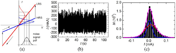
Figure 5. (a) Analysis of the current response of the memristor to Gaussian white noise; (b) waveform; (c) distribution histogram of the current flowing through a memristor I in the noise-induced RS mode ( V;
V;  V), for LRS (red curve), HRS (blue curve) and superposition (purple curve).
Download figure:
Standard image High-resolution imageTaking into account all the above, in the present study the state of the memristor at a given time t is characterized by the mean resistance  where
where

is the standard deviation of I calculated for a short time period  ,
,  is the averaged current over the time period Ta, and M = 100 is the number of points in the time series of the current I, measured within the period Ta.
In figure 6 three waveforms  calculated, according to the procedure described above for the memristor in the noise-induced RS mode, at different values of the noise signal parameters, are shown. As one can see from figure 6, the waveforms
  demonstrate typical RTS shape. In the middle panel of figure 6, the corresponding probability density functions (PDFs) of R are presented. The PDFs manifest bi- or trimodal distributions of R subject to the noise parameters that corresponds to the switching of the memristor between 2 or 3 metastable states under the noise signal. The right panel of figure 6 shows the effective potential profiles of the memristor, calculated from the respective probability distributions of R in the central panel, using the standard procedure usually applied for nonlinear systems whose dynamics is described by the Langevin equation with a multiplicative noise [43–45]. Indeed, the voltage-controlled memristive systems are defined by the Langevin equations [35]
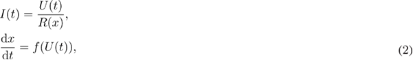
where  is the controlling parameter describing the internal state of the system,
  is a random voltage across the device varying in time, that is a stochastic voltage, and
  is some threshold function. From equation (2) we arrive at the following Langevin equation for the resistance

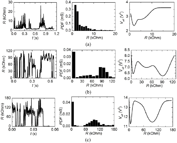
Figure 6. Waveforms (left) and corresponding PDFs (middle) of the memristor resistance R in the noise-induced RS mode.  , V.
, V.  ,
,  (a), 0.75 (b), 1.0 (c). The right panel shows the effective potential profiles of the memristor calculated from the corresponding PDFs of R.
Download figure:
Standard image High-resolution imageAs it can be seen from equation (3), the stochastic voltage  applying to the memristor is always multiplicative. As a result, one can introduce the effective potential profile
  through the stationary PDF
  of the resistance for the white Gaussian noise
  with the intensity 2D by the following relation [43–45]

where  is a normalization constant. We note that the standard technique of extracting the potential profile of a system from its response to the white noise signal is applicable when the system is in a steady state [43–45]. Actually, the memristor changes its electrical parameters during the experiments, and rigorously the above approach appears to be non-applicable. However, one can postulate that over a large time scale such that
  , the averaged state of the memristor should change rather slowly, having reached a quasi-stationary state. In this case, one can consider the effective potential profile of the memristor in a quasi-static state and than trace the long-time scale evolution of the memristor. Similar approach has been applied by Slipko with co-workers [35].
The effective potential profiles manifest 2 or 3 local minima, corresponding to the number of peaks in the R distribution histograms shown in the middle panel of figure 6, with different depths and widths of the potential wells. One can see that the shape of the potential profile, particularly, the number of local minima appears to depend on the noise parameters. For example, at  V, there are two local minima on the potential profile (see figure 6(c)) whereas at
  V, a three-well potential has been observed (figure 6(b)) corresponding to the number of the levels of R observed in the respective waveforms of
  (see the left panels of figure 6(b)). It is worth noting that the three-well potential was predicted for a memristor earlier [36, 40], as it has been already mentioned above (see section 1 for details). At
  V, the barrier between the potential wells disappeared, actually only one minimum was observed in the potential profile (figure 6(a)).
In accordance with equation (4), the dependence of the effective potential profile of the memristor on the input noise parameters reveals the multiplicative character of the noise on the memristor switching dynamics, in other words the noise perceived by the memristor depends on the state of the system [45] and its electrical properties are influenced by the noise signal. Therefore, the potential profiles shown in figure 6 could be considered as quasi-effective potentials. The effective potential profiles of the investigated memristor are found to change during the experiment on study of the memristor's response to the noise signal. In figures 7(a) and (b), the long-time-scale waveforms  and
and  of the memristor in the noise-induced RS regime are shown. The RTS patterns are changing in the course of the experiment. Four examples of different
  and
and  waveform patterns, recorded in selected time windows during the records shown in figure 7 with corresponding PDFs of R, are shown in figure 8. First, the averaged (in the long-time-scale
  ) memristor resistance increases gradually (see the beginning of the waveforms in figure 7), and this behavior can be interpreted as the degradation of the memristor. However, afterwards the noise-induced RS mode restored abruptly. Earlier, it was shown that the RS of a memristor can be restored after complete degradation by applying a suitable electrical signal [46]. The results of the present study demonstrate the restoring of RS by a noise signal.
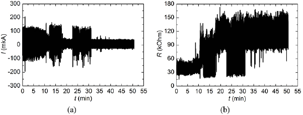
Figure 7. Long-time-scale waveforms  (a) and
  (b) for the memristor based on a ZrO2(Y)/Ta2O5 stack under Gaussian white noise signal with
  V and
V and  V.
V.
Download figure:
Standard image High-resolution image
Figure 8. Waveforms  (left) and
  (middle) recorded in different time windows during the experiment on study of the memristor's response to the white Gaussian noise signal: 0–5 min (a), 10–15 min (b), 20–25 min (c), and 35–40 min (d).
  V,
V,  V; corresponding distribution histograms of R (right).
Download figure:
Standard image High-resolution imageThe abrupt degradation and restoring of the memristor have been observed several times during the experiment (see figure 7). Note that the RTS patterns changed suddenly as well (see, for example, figures 8(b) and (c)). The observed sudden changes in the behavior of the memristor during the experiment may be interpreted as a result of sudden change of the electrical properties of the memristor under the external noise signal. Burning out of the active filament and the wakeup of the next potential filament can be one of such sudden events [47, 48]. Finally, the memristor has frozen in the HRS, which corresponds to its complete degradation (figure 8(d)).
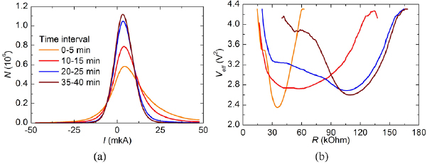
In figures 9(a) and (b), the time evolution of the current distribution histograms and of the effective potential profile of the memristor during the experiment are shown respectively. The evolution of the effective potential profiles reflects the changes of the electrical properties of the memristor during the experiment under the impact of the noise signal. Correspondingly, the distribution of I changes in time (figure 9(a)). These observations confirm the multiplicative character of the noise signal on the dynamical behavior of the memristor. Note that the final state of the memristor is represented by a simple effective potential with a single potential well.
Figure 9. The time evolution of the current distribution histogram (a) and of the effective potential profile (b) of the memristor during the experiment.
Download figure:
Standard image High-resolution image
4. Conclusions
In the present study, we have investigated experimentally the response of a memristor based on ZrO2(Y)/Ta2O5 stack to a white Gaussian noise signal. A stochastic switching of the memristor between two or three metastable resistance states in the random telegraph signal mode has been observed. Such peculiarity is inherent to the dynamical behavior of multistable systems subjected to an external noise. The potential profiles extracted from the waveforms of the current response of the memristor to the white Gaussian noise signal manifests from two to three local minima, corresponding to the number of levels of the memristor resistance switching observed in the experiment. The obtained experimental results evidence the applicability of the statistical physics formalism, applied usually to the description of the behavior of multistable nonlinear systems, to the dynamical switching behavior of memristors. Moreover, the potential profiles of the memristors are found to depend on the magnitude of the input noise signal that indicate the multiplicative character of the noise on the dynamical behavior of the memristor, that is the noise perceived by the memristor depends on the state of the system and its electrical properties are influenced by the noise signal. Furthermore, the evolution of the potential profile of the memristor was studied under the white Gaussian noise signal. It has been discovered that the potential profile of the memristor changes abruptly this indicates the sudden changes in memristor properties under the impact of noise. The effect of noise on the electrical properties of the memristor was attributed to the burning out of the active filaments and the wakeup of the potential ones. The results of the present study indicate the memristors to be more complex dynamic system than in a system with a simple two-well potential profile. To develop a more adequate theoretical description of the real memristor on the basis of a statistical physics approach, a further development of the theory and further experiments on its verification are needed.
Also, it shold be noted that the approach based on the analysis of the response of a memristor to an artificial noise signal is applicable not only to the oxide-based memristor utilizing the filametrary RS mechanism (which were the subjects of investigations in the present study) but also to the memristors based on other RS types, such as conducting bridge (CB) or interface RS. The investigations of the above types of memristors will be the subject of future research.
Acknowledgments
This work was supported by the Government of the Russian Federation, Agreement No. 074-02-2018-330 (2).