

Abstract
This paper presents the implementation of an electronic fully-digital impedance bridge optimized for RC comparisons with equal impedance magnitudes, together with an evaluation of the uncertainty. This bridge has been designed with the goal of realizing the farad directly from the quantum Hall effect with a bridge uncertainty component at the 10−7 level. Thanks to its simple design, ease of operation and affordability, this bridge is suitable to be industrially manufactured. Together with the increasing availability of graphene quantum Hall resistance standards, this can provide an affordable quantum realization of the unit farad for metrology institutes and calibration centres.
In this paper we present the uncertainty budget of an example measurement and the results of the validation of the bridge against a suitably modified version of the traceability chain of the Italian national standard of capacitance. The combined uncertainty of the bridge resulted from repeated measurements (overall measurement time of about 200 min) is 9.2 × 10⁻⁸, suitable for the primary realization of the unit of capacitance from a quantized Hall resistance standard. The crosstalk among the channels of the electrical generator is the most significant uncertainty component, possibly reducible with internal shielding and filtering of the electronic generator.
Export citation and abstract BibTeX RIS

Original content from this work may be used under the terms of the Creative Commons Attribution 4.0 license. Any further distribution of this work must maintain attribution to the author(s) and the title of the work, journal citation and DOI.
1. Introduction
In the International System of Units (SI), the units of electrical impedance ohm, henry and farad are linked by the relations  . Since the 2018 revision of the SI,
The farad F can be realized [...] by comparing the impedance of a known resistance obtained using the quantum Hall effect and the value of the von Klitzing constant [...], including a quantized Hall resistance itself, to the impedance of an unknown capacitance using, for example, a quadrature bridge; [...] [1, appendix 2]
The quadrature bridge mentioned in the SI brochure is a double product impedance bridge [2, 3], which compares two resistors R1 and R2, and two capacitors C1 and C2, at a properly chosen fixed angular frequency ω. The standard implementation of the quadrature bridge principle [4–8] results in a very complex electrical network with many electromagnetic components, including several multi-decade inductive voltage dividers. These variable dividers must be skilfully operated in order to achieve both the two main balances and, simultaneously, several auxiliary ones. The latter are in fact required to match the proper impedance definition of each of the four standards being compared. Automating the quadrature bridge, although possible, is cumbersome [9, 10]. Digitally-assisted implementations [11, 12] can reduce the network complexity of the quadrature bridge to some extent, and allow a partial automation. A quadrature bridge calibrates the product  ; an additional measurement with a ratio bridge is required to determine the individual values of C1 and C2.
The quoted SI brochure entails that R1 and R2 are either resistance standards having an AC value traceable to a quantized Hall resistance (QHR) standard, or that they are QHR standards themselves, measured in the AC regime (ACQHR standards). In the first case [12–14], special resistors having a calculable frequency dependence [15, 16] are calibrated in DC versus the QHR, and their values are numerically corrected. In the second case [6, 17], the effect of unwanted frequency dependencies caused by parasitic effects in the Hall device must be carefully considered [18, 19]. To date, only one laboratory worldwide operates a permanent quadrature bridge with two quantum Hall effect devices in a single cryostat [17], a massive and complex experiment filling an entire laboratory.
Fully-digital bridges [20–25] can compare a single resistor R and a single capacitor C. The fully-digital approach allows the design and implementation of much simpler bridges suitable to be industrially manufactured. Together with the increasing availability of quantum Hall graphene devices, which allow the realization of QHR standards in simpler experimental environments [26], the fully-digital approach underpins an affordable quantum realization of the unit farad by metrology institutes and calibration centres [27].
In the following, we present an electronic
4
fully-digital bridge suitable for the realization of the farad
5
. The bridge calibrates a capacitance standard of nominal value 8 nF versus a resistor R of nominal value  at the frequency
6
f ≈ 1541 Hz.
at the frequency
6
f ≈ 1541 Hz.
The bridge network is very simple and is based on a multi-channel polyphase electronic digital waveform generator [33]. The bridge balance is semi-automated, and the duration of an individual measurement is around 15 min. The transfer relative expanded uncertainty is about 3 × 10⁻⁷ in a single measurement (15 min) and down to 2 × 10⁻⁷ in about 5 measurements (75 min).
This work reports the principle of operation of the bridge (section 2), its implementation (section 3), a thorough analysis of the uncertainty sources (section 4), and a validation of the bridge performance, by comparison with the traceability chain of the Italian national standard of capacitance [12] (section 5).
2. Principle of operation
The four-terminal-pair voltage-ratio fully-digital impedance bridge described herewith is based on the principle schematic of figure 1, where the coaxial shield and terminal pairs, and a number of auxiliary components have been omitted for simplicity (the complete schematic is reported in section 3).

Figure 1. Simplified principle schematic of the bridge:  and
and  are the impedances under comparison; f is the bridge operating frequency, chosen so that 2π
f
RH
C ≈ 1; E1 and E2 are the main bridge voltages; I1 and I2 are the current sources balancing IHP1 and IHP2; EL is the voltage source balancing the difference
are the impedances under comparison; f is the bridge operating frequency, chosen so that 2π
f
RH
C ≈ 1; E1 and E2 are the main bridge voltages; I1 and I2 are the current sources balancing IHP1 and IHP2; EL is the voltage source balancing the difference  ; CT1 and CT2 are current transformers measuring the currents IHP1 and IHP2, respectively; the voltage source E0 and the impedance Z0 constitute an auxiliary injection arm to fine-tune the bridge balance; and D is a synchronous detector that can be connected, in turn, to the detection terminals LP1, LP2, DHP1 and DHP2. The diagrams on the left represent example waveform samples: the samples of E1 are changed in sign between the forward and reverse configurations; the samples of E2 are instead kept fixed.
Download figure:
Standard image High-resolution imageThe driving voltages and currents E1, E2, E0, EL, I1 and I2 are synthesized by a polyphase digital sinusoidal waveform generator operating at frequency f and can be individually adjusted in magnitude and phase 7 . Each voltage or current corresponds to an output channel of the generator. E1 and E2 are the bridge main voltages; EL, I1 and I2 are auxiliary voltage and currents needed to realize the impedance definition; and E0 is an auxiliary injection voltage which, together with the injection impedance Z0, allows to fine-tune the bridge balance.
The impedances under comparison are Z1, with terminals HC1, HP1, LC1 and LP1, and Z2, with terminals HC2, HP2, LC2 and LP2. In this specific application, Z1 is the reference impedance that can be either an ACQHR standard with resistance RH, connected with a multiple-connection scheme (see section 6), or a calibrated standard resistor with nominal resistance RH, such that  ; Z2 is a capacitor with capacitance C, such that
  ; and f is chosen so that 2π
f
RH
C ≈ 1 (that is,
; and f is chosen so that 2π
f
RH
C ≈ 1 (that is,  ).
).
The bridge is balanced when  and
and 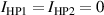 , where the voltages VLP1 and VLP2 are measured at the impedance terminals LP1 and LP2, and the currents IHP1 and IHP2 are measured at the detection terminals DHP1 and DHP2 through the current transformers CT1 and CT2. The balance can be checked by cycling the synchronous detector D, referenced at the frequency f, through the detection terminals LP1, LP2, DHP1 and DHP2, and can be attained by adjusting E2 (or E1), E0, EL, I1 and I2 (the details of the balance procedure are discussed in section 3).
When the bridge is balanced, the impedance ratio  is directly compared with the voltage ratio
  , and the following balance equation holds:
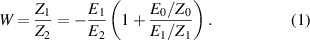
Alternatively, by considering the admittances  ,
,  and
and  ,
,
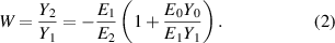
As can be seen from the above equations, by choosing  , the voltage E0 can be used to fine-tune the bridge balance around the ratio
  . This is instrumental to achieve the highest measurement accuracy, as described below.
The voltage phasors E1 and E2 can be computed from the samples used to synthesize the two waveforms. We take the readings  and
and  from the fundamental components at frequency f of the Fourier series representing the waveform samples. Due to the generator non-idealities, the actual voltages will differ from the readings and we can write
 ![$E_k = [1+g_k(E_k^{\,\textrm{read}})]E_k^{\,\textrm{read}}$](https://content.cld.iop.org/journals/0026-1394/58/1/015002/revision3/metabba86ieqn21.gif) , k = 1, 2, with
, k = 1, 2, with  representing a possibly voltage-dependent complex gain error (for magnitude and phase errors), thus considering a possible generator non-linearity. This is actually the main source of error in fully-digital bridges [23, 34].
The error described above can be perfectly cancelled by performing two measurements: one with the impedances connected as in figure 1 (forward configuration) and one with the two impedances exchanged (reverse configuration), and by imposing that the samples used to generate E1 and E2 are exactly the same in the two configurations, at most shifted in time, as shown on the left of figure 1 (how this condition can be imposed is described in section 3). This is feasible because with the conditions introduced at the beginning of this section, the magnitude of the impedance ratio is about 1 in both the forward and reverse configurations, 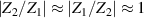 , and its phase changes by about 180° because
  . Therefore, to balance the reverse configuration, we just need to change the sign of all the samples of either E1 or E2 (equivalent to a 180° shift), and re-adjust the injection voltage E0.
For the forward (F subscript) and reverse (R subscript) configurations, the balance equations are
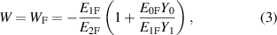
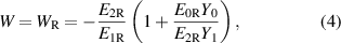
from which

where the complex square root in (5) should be determined with a positive imaginary part because  .
.
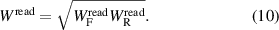
According to the foregoing argument, 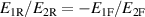 , exactly, by construction of the waveform samples, such that, from (3)–(5),
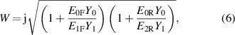
thus cancelling any major error due to  (minor errors are discussed in section 4).
From W and the reference impedance Z1, the capacitance C can be finally determined as
where  denotes the imaginary part of its argument.
3. Bridge implementation
Figures 2 and 3 show the coaxial schematic and a photograph of the bridge.

Figure 2. Coaxial implementation of the principle schematic diagram of figure 1. Injection/detection transformers provide the voltage  and the detection of VDHP1 and VDHP2. Each black rectangle represents a coaxial equalizer.
Download figure:
Standard image High-resolution image
Figure 3. Picture of the experimental set-up.
Download figure:
Standard image High-resolution imageThis section describes only the implementation of the bridge network; the impedances Z1 and Z2 employed in the validation are described in section 5.
At the core of the bridge there is the adjustable polyphase digital sinusoidal waveform generator described in [35] 8 . This digital signal source is based on 18 bit digital-to-analogue converters with adjustable range (1 V, 2.5 V, 5 V and 10 V) and isolated precision filter/buffer output stages [37]. The relative amplitude and phase stability of the source are about 10−7h−1. A National Instruments NI-DAQ 6541 board generates the digital codes of the waveform samples, which are then transmitted to the source. The waveform is composed of a fixed integer number of samples per period 9 and the frequency is adjusted through the sample rate and the number of samples. This yields the possibility to control the output samples and obtain a simple and computable output spectrum. A channel reading is then obtained from the latter. The clock of the digital source, which defines the sample rate, is locked to a 10 MHz signal from the Italian national time scale.
The digital source provides seven independent output channels, necessary for the complete implementation of the bridge. Two channels generate the voltages E1 and E2, which provide the voltage ratio reference against which the impedance ratio is compared. The 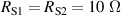 resistors (Vishay S102 series), in series to E1 and E2, isolate the channel outputs from the capacitive load, avoiding possible self-oscillations of the output buffers.
Three channels generate the voltages E3, E4 and EL which drive the auxiliary circuits realizing the four terminal-pair impedance definition. The currents I1 and I2 are generated by E3 and E4 through the 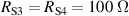 resistors (Vishay S102 series). Two dummy loads CL ≈ C and
  are added at the HC ports of the impedances to symmetrize the source loading in both forward and reverse configurations.
One channel generates the voltage EL through a 200 : 1 feedthrough injection voltage transformer. One channel generates the voltage E0 which provides the auxiliary injection through the C0 = 1 pF capacitor, which corresponds to Z0 in figure 1. One further channel generates the reference signal for the phase-sensitive detector.
The phase-sensitive detector is a Stanford Research SR830 lock-in amplifier and is used to detect the bridge balance on the fundamental component of the signal.
The detector is manually switched across the positions VDHP1 and VDHP2, measuring the currents IHP1 and IHP2 through the 1:200 feedthrough transformers CT1 and CT2, and the positions VLP1 and VLP2.
Both the digital source and the detector are controlled by a software purposely coded in the National Instruments LabWindows/CVI environment and based on the balancing algorithm presented in [39]. The bridge balance procedure is thus semi-automated and a single complete measurement (forward/reverse) requires about 15 min. According to what was introduced in section 2, when switching between the forward and reverse configurations, we can change the phase of E1 by 180° and keep E2 fixed. The digital source employed in this implementation allows to read the generated samples verifying that they are exactly matched with a 180° phase shift.
Before beginning a series of measurements, it is convenient to preset the main voltages E1 and E2 to minimize the auxiliary injection E0. Starting from the set-up shown in figure 2, the preliminary procedure can be done in the following way:
- P1.Set E0 to 0 V, and E1 to the operating value of interest.
- P2.Short circuit both VLP1 and VLP2.
- P3.Adjust E3 to null the detector connected to VDHP1.
- P4.Adjust E4 to null the detector connected to VDHP2.
- P5.Remove the short circuit at VLP1.
- P6.Adjust E5 to null the detector connected to VLP1 (this actually nulls the differential voltage
 ).
). - P7.Remove the remaining short circuit at VLP2.
- P8.Adjust E2 to null the detector connected to VLP1.
- P9.Adjust E4 to null the detector connected to VDHP2.
- P10.Repeat steps P8 and P9 until the detector is nulled simultaneously within the chosen thresholds for both detection ports.
- P11.Record the voltage reading for the forward configuration.
- P12.Change set-up from the forward configuration to the reverse one by swapping the cables between and , and by shifting the phase of E1 by 180°.
- P13.Repeat steps P1 through P10 and record the voltage reading for the reverse configuration.
- P14.Set E2 in both configurations to the geometric mean.


The measurement procedure is then as follows:
- M1.In the forward configuration, execute the steps P2 through P7 of the preliminary procedure and finally adjust E0 to null the detector connected to VLP1. Record the readings, and .
- M2.In the reverse configuration, execute the steps P2 through P7 of the preliminary procedure and finally adjust E0 to null the detector connected to VLP1. Record the readings, and .
- M3.
- M4.The capacitance C is determined, from W and the impedance Z1, as in (7).


We note the following: i) even though the bridge balance procedure can be completely automated with an external switch, we preferred the semi-automated approach to avoid the risk of worsening the crosstalk between the source channels (see section 4.2); and ii) the steps P5 and P6 of the preliminary procedure can be substituted with a measurement with the detector set in the differential input configuration.
4. Uncertainty sources and budget
This section presents an evaluation of the uncertainty for the ratio  as defined by (5). The uncertainty sources are first described separately and then the relevant ones are combined in a measurement model which is used in reporting the uncertainty budget (for a review on the error sources in digital impedance bridges see also [34]).
In the following, according to the notation introduced in section 2, the subscripts 'F' and 'R' designate quantity values obtained in the forward and reverse configurations, respectively; the superscript 'read' designates quantity values read off the generator settings, as described in section 1. From (3)–(5) we also define
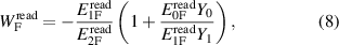
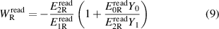
and
4.1. Type A uncertainty
In this experiment, the type A uncertainty mainly depends on the noise at the detection ports LP1, LP2, DHP1 and DHP2, on the mutual impedance Zm of the current transformers CT1 and CT2, on the detector time constants and thresholds chosen to stop the bridge balancing at the various detection ports, and on the instabilities of the source and the standards.
The contribution of the low balance to the type A uncertainty component of W, for a single measurement, should be expected of the order of  , δ
VL being the spread of the residual voltages at LP1 and LP2. The contribution of the high balance should be expected of the order of
, δ
VL being the spread of the residual voltages at LP1 and LP2. The contribution of the high balance should be expected of the order of  , δ
VH being the spread of the residual voltages at DHP1 and DHP2 (see [34] for a more detailed analysis).
, δ
VH being the spread of the residual voltages at DHP1 and DHP2 (see [34] for a more detailed analysis).
For the current setup we set the thresholds for the balances at LP1 and LP2 to 30 nV (1 s detector time constant) and the thresholds for the balances at DHP1 and DHP2 to 200 nV (300 ms detector time constant). With these settings, taking into account that  , the projected type A uncertainty component is about 10−7 for a single measurement.
4.2. Crosstalk
Crosstalk is the phenomenon by which the voltage at one channel of the polyphase generator is coupled to that of another channel. Considering just the channels that may induce significant variations when switching between the forward and reverse configurations, and that  and
and  , we can therefore write


In the above equations, E10 and E20 represent possible residual voltages at the source outputs, independent of  and
and  , and which can be due to the crosstalk from
  or a clock feedthrough; and aij
is the (complex) coupling coefficient from channel j to channel i.
or a clock feedthrough; and aij
is the (complex) coupling coefficient from channel j to channel i.
Due to crosstalk, the equality  , obtained in section 1 from the construction of the samples, no longer holds exactly. As a consequence, an error arises. By combining (11) and (12) with (3)–(5), and simplifying, we obtain at first order in the coupling coefficients

with the error ΔWCT given by
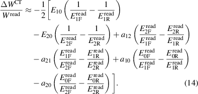
The measured average magnitudes of E10 and E20 are of the order 30 nV, with a high phase uncertainty. For a reasonably conservative evaluation of the uncertainty, for E10 and E20, we assumed uncorrelated real and imaginary parts centred around 0 with a standard uncertainty of 30 nV for each part, corresponding to a square coverage region. The measured magnitudes of the coupling coefficients between the different channels of the polyphase generator are less than 2 × 10⁻⁸, with a high phase uncertainty. For these coefficients, we assumed uncorrelated real and imaginary parts centred around 0 with a standard uncertainty of 2 × 10⁻⁸ for each part.
4.3. Injection uncertainty
The injection terms in (3) and (4) depend on the voltage ratios  ,
,  and on the admittances Y0 and Y1. The voltage ratios can be written as
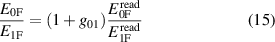
and
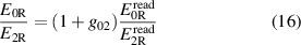
where the complex error terms g01 and g02 account for the generator non-linearity as described in section 1.
A characterization of the source yielded for 1 + g01 and 1 + g02 a magnitude uncertainty of about 10−4 and an angle uncertainty of about 10−4 rad. The uncertainty contributions of Y0 and Y1 are typically negligible.
4.4. Source loading
When the bridge is balanced, the currents crossing CT1 and CT2 are approximately zero, but E1 and E2 are still loaded by the stray capacitances CH1 and CH2 of the cables connecting the channels to the current transformers.
When reversing the channels at the source ports, as is done in this experiment, this causes an error such that [23, 34]


where YH1 and YH2 are the admittances of CH1 and CH2, respectively. If the bridge construction is symmetric, the difference  is small. Since
  , the expression in the brackets changes at first order only the real part of
  and not its imaginary part. Therefore, from (7), the resulting error on C is negligible at the target uncertainty level of this experiment and will not be considered in the measurement model of the next section.
4.5. Measurement model and uncertainty budget
By combining the above results with (6), we obtain the measurement model
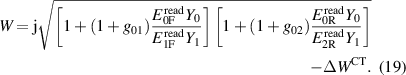
Table 1 reports the uncertainty budget of an example measurement for the quantity  (because
  ). All the uncertainties are standard uncertainties (k = 1). The measurement was performed on 20 February 2020 and it is also discussed in section 5.1. The driving rms voltages
 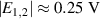 are chosen so that the driving current I ≈ 20 µA flowing in the standards is suitable for the QHR. We performed the propagation of uncertainty according to [40] with the help of Metas.UncLib [41].
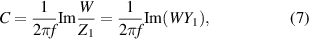
Table 1. Example uncertainty budget for Δ = ImW − 1. All the uncertainties are standard uncertainties (k = 1).
| i | Quantity | Type |

|
|---|---|---|---|
| 1 | Bridge reading (n = 13) | A | 0.022 |
| 2 | Crosstalk (ΔWCT) | B | 0.089 |
| 5 | Injection | B | 0.01 |
| RSS | 0.092 |
The measurement consisted in n = 13 repetitions of forward and reverse measurements, for an overall measurement time of about 200 min and a type A uncertainty component of 2.2 × 10⁻⁸, in reasonable agreement with the value obtainable from the projection of section 4.1 (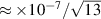 ). The most significant uncertainty component is that associated to ΔWCT, which was evaluated from (14) and the measurements of the coupling coefficients.
The combined uncertainty is 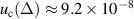 , which is competitive for the primary realization of the unit of capacitance. Since the type A uncertainty is much smaller than the type B, 5 measurements are enough to reach a combined uncertainty of 2 × 10⁻⁷.
5. Validation
The validation of the bridge performance was obtained by comparing the 8 nF capacitor calibration performed with the four-terminal-pair fully-digital bridge with that performed with the traceability chain of the Italian national standard of capacitance [12]. The latter is typically employed to calibrate a 1 nF capacitance standard against a calibrated 12 906 Ω quadrifilar resistance standard, but it is here adapted to calibrate the 8 nF capacitance standard.
Figure 4 shows the measurement chain adopted in the validation process.

Figure 4. Diagram of the procedure adopted to compare the calibration of the 8 nF capacitance standard performed with the four-terminal-pair fully-digital bridge and that performed with the traceability chain of the Italian national standard of capacitance.
Download figure:
Standard image High-resolution imageOn one side of the chain, two resistance standards R1 and R2 of nominal value 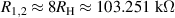 are calibrated with a 8:1 transformer-ratio resistance bridge against a resistance standard of nominal value
  . These resistance standards are then employed in a transformer-ratio quadrature bridge to calibrate the product
  of two 1 nF capacitance standards. By means of a double calibration of the 8 nF capacitance standard against C1 and C2 with a 1:8 transformer-ratio bridge,
  is then obtained from the product
  .
.
On the other side, the calibration Cfd of the 8 nF is performed with the four-terminal-pair fully-digital bridge against the same 12 906 Ω resistance standard employed before, as described in section 3.
The two calibrations are performed at the same operating frequency of 1541.4326 978 Hz and current of 20 µA. This frequency is chosen to minimize the injections of both the fully-digital bridge and the quadrature bridge. For the fully-digital bridge, the residual deviation from the optimum condition  is about 3.5 × 10⁻⁵.
During the measurement procedure, the 8 nF capacitance standard is kept in a temperature-controlled chamber (Kambič TK-190 US) with a temperature stability better than 4 mK [42]. Since the temperature coefficient of the capacitance standard is  C−1 [43], the maximum effect due to the temperature dependence is about 4 × 10⁻⁸ and can be considered virtually negligible with respect to the other uncertainty components. However, even though hermetically sealed in dry nitrogen, the 8 nF capacitance standard shows a significant dependence on the atmospheric pressure [44], evaluated in section 5.1.
5.1. Results
The result of the comparison is the relative difference
Figure 5 reports the results of the comparisons performed on 17 and 20 February 2020. Each point in the plot represents the result of the comparison of the average of two successive measurements of Cfd with one measurement of  .
.

Figure 5. Comparison between the calibrations of an 8 nF capacitance standard performed with the four-terminal-pair fully-digital bridge described in the paper and with the Italian capacitance traceability chain, suitably modified. The plot represents the quantity  .
.
Download figure:
Standard image High-resolution image
For the setup of 17 February, the thresholds were set to 50 nV for the balances at LP1 and LP2 and to 500 nV for the balances at DHP1 and DHP2. For the setup of 20 February, the thresholds were set to 30 nV for the balances at LP1 and LP2 and to 200 nV for the balances at DHP1 and DHP2. The latter set of parameters lead to an improved repeatability and it will be therefore considered an optimal trade-off between repeatability and balancing time.
The dependence on the atmospheric pressure of the 8 nF capacitance standard, introduced in section 5, is checked at regular time intervals with an ultra-precision capacitance bridge (Andeen-Hagerling 2700A). The instability component of the capacitance standard is thus considered for each measurement in the uncertainty of δ, which is calculated by combining the uncertainties of Cfd and  . The expanded uncertainty of
  is
is  , higher than the one stated in [12] to take into account the adaptation of the measuring chain.
In figure 5, the uncertainty bars represent the expanded uncertainties with coverage factor k = 2.
For the measurements of 20 February, the mean value is δ ≈ 3.0 × 10⁻⁷ with an expanded uncertainty U(δ) ≈ 2.9 × 10⁻⁷.
6. Conclusions and outlook
We presented the design, the implementation and the uncertainty evaluation of a four-terminal-pair fully-digital impedance bridge, optimized for RC comparisons with 1:1 magnitude ratio. Here the bridge was applied to compare a resistance standard with nominal value of RH with an 8 nF capacitance standard at 1541 Hz (a 10 nF standard capacitor can be for instance measured at 1233 Hz). We reported the uncertainty budget of an example measurement consisted in 13 repetitions of forward and reverse measurements (overall measurement time of about 200 min). The type A uncertainty component is of 2.2 × 10⁻⁸, while the most significant uncertainty component is that associated to the crosstalk among the channels of the generator, which is about 8.9 × 10⁻⁸. The combined uncertainty is 9.2 × 10⁻⁸, suitable for the primary realization of the unit of capacitance from a QHR standard. It should be noted that, since the type A uncertainty component is much less than the type B component, 5 measurements (overall measurement time of about 75 min) are enough to reach a combined expanded uncertainty of 2 × 10⁻⁷. The bridge was validated against a suitably modified version of the traceability chain of the Italian national standard of capacitance.
This bridge is intended to be a much simpler, easy-to-operate and affordable alternative to traditional bridges, suitable to be industrially manufactured. Together with the increasing availability of graphene quantum Hall resistance standards, this can provide an affordable quantum realization of the unit farad for metrology institutes and calibration centres. The accuracy can be further improved by means of internal shielding and filtering of the generator to reduce the crosstalk among the channels.
To employ this bridge with a QHR standard it is necessary to adopt a multiple-connection scheme [45] and possibly a double-shield technique [46]. The integration of the bridge with a QHR standard will be the subject of a future work.
Acknowledgment
This project (18SIB07 GIQS) received funding from the European Metrology Programme for Innovation and Research (EMPIR) co-financed by the Participating States and from the European Unions' Horizon 2020 research and innovation programme.
Footnotes
- 4
- 5
This paper is focussed on the bridge description and on its measurement capabilities; its integration with a quantum Hall effect system is under development and will be reported in a future work.
- 6
The nominal values for C and f are chosen to fulfil the relationship 2π f R C ≈ 1. The integer value C = 8 nF = 23 nF allows efficient scaling to the decadal values of interest for dissemination; the frequency f ≈ 1541 Hz is close to 1592 Hz≈10 kHz/(2π), a de facto standard frequency for capacitance dissemination and intercomparisons [32].
- 7
In the following, quantity symbols represent complex phasors associated to real voltage and current signals, or complex impedances.
- 8
The generator was developed by Janusz Kaczmarek and Ryszard Rybski, University of Zielona Góra (UZG), Poland, in the framework of the European project EMRP SIB53 AIM QuTE: Automated impedance metrology extending the quantum toolbox for electricity [36].
- 9
Unlike what happens in a direct-digital synthesizer (DDS) with phase accumulation [38].