
Abstract
This review article discusses the development of gallium arsenide (GaAs)-based resonant tunneling diodes (RTD) since the 1970s. To the best of my knowledge, this article is the first review of GaAs RTD technology which covers different epitaxial-structure design, fabrication techniques, and characterizations for various application areas. It is expected that the details presented here will help the readers to gain a perspective on the previous accomplishments, as well as have an outlook on the current trends and future developments in GaAs RTD research.
Export citation and abstract BibTeX RIS
1. Introduction
The pioneering work of Leo Esaki and Raphael Tsu[1−3] has led resonant tunneling diode (RTD) to come into recognition. Esaki, during his PhD days (in 1958) reported on a new diode (named the Esaki or tunnel diode) that exhibited negative resistance in its current–voltage (I–V) characteristic, and which was used for microwave communications, high-frequency amplifier, logic circuits, and oscillators[4−11]. Although this diode was faster than the conventional diodes and transistors, it was hard to use in control circuits, and was also expensive. In 1973, Esaki and Tsu reported a new tunneling phenomenon in a superlattice. It was observed from the computed I–V characteristic that multibarrier tunneling model would provide better understanding in observing the transport mechanism for a superlattice having limited number of spatial periods or a short mean free path. A year later, in 1974, Chang Tsu and Esaki demonstrated a device based on their previous collaborative work and theories—the RTD. RTD is a semiconductor device that utilizes quantum mechanical tunneling to transport electrons through a thin barrier in the device. The tunneling effect occurs when the energy of the electron is less than the height of the energy barrier, which allows the electron to pass through the barrier without losing any energy. In an RTD, the tunneling effect is enhanced by the presence of a resonant state in the barrier material. This resonant state allows the electrons to tunnel through the barrier more easily, resulting in a peak current that occurs when the energy of the incoming electrons matches the energy of the resonant state. The physics of a RTD can be described by the resonant tunneling mechanism, which involves the coupling of two resonant states in the barrier material. When an electron enters the RTD, it encounters the first resonant state and tunnels through the barrier, entering the quantum-well region of the device. The electron then encounters the second resonant state and tunnels through the second barrier, exiting the device.
RTD typically consists of a quantum well (made from a semiconductor having a smaller bandgap) that is sandwiched between two potential barriers (made from a semiconductor with a larger bandgap). This means that the basic configuration of an RTD is a double-barrier quantum-well (DBQW) structure. When the two-terminal RTD device is biased, electrons having lower kinetic energy than the barriers may tunnel through the DBQW structure. The possibility of electrons tunneling through the barriers is defined by the transmission coefficient. At the resonant state, the transmission coefficient is close to unity. As the transmission coefficient of electrons tunneling through the DBQW changes with the bias voltage, the current–voltage (I–V) characteristic of the RTD device exhibits negative differential resistance (NDR)[3, 12−14]. The energy band diagram of a typical double-barrier RTD structure and the corresponding I–V characteristics are shown in Figs. 1 and 2, respectively, where Ec is the conduction band energy, Ef is the Fermi energy, and E1 and E2 are the quantization energies; Ip, Iv, Vp, and Vv are the respective peak and valley current and voltages. Fig. 1(a) is the band diagram with no external bias; no current flows in this condition and the quantized states E1 and E2 inside the well are larger than the Fermi energy Ef. At small bias voltage (Fig. 1(b)), some current starts flowing through the device as the electrons gain sufficient energy to overcome the barriers. On further increasing the bias voltage and when the electron energy coincides with the quantized state energy E1 (Fig. 1(c)), resonant tunneling occurs. At resonance (i.e., when the energy levels are equal), there will be more electrons flowing through the barriers and this will result in a peak current Ip. If the bias voltage is increased further, and first resonant energy falls below the conduction band offset (Fig. 1(d)), there will be a sudden drop in current (due to the off-resonance condition) resulting in an NDR regime. The current will continue to drop on further voltage increment (Fig. 1(e)) and will again start rising with increasing voltage when the second resonant energy level falls below the Fermi level energy (Fig. 1(f)).
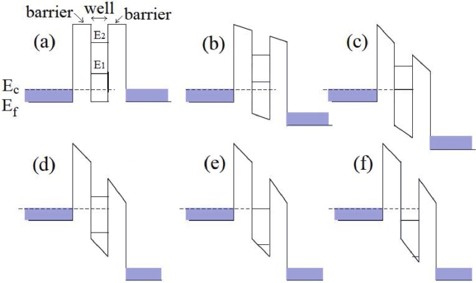
Fig. 1 (Color online) Energy band diagram of a typical double-barrier RTD structure.
Download figure:
Standard image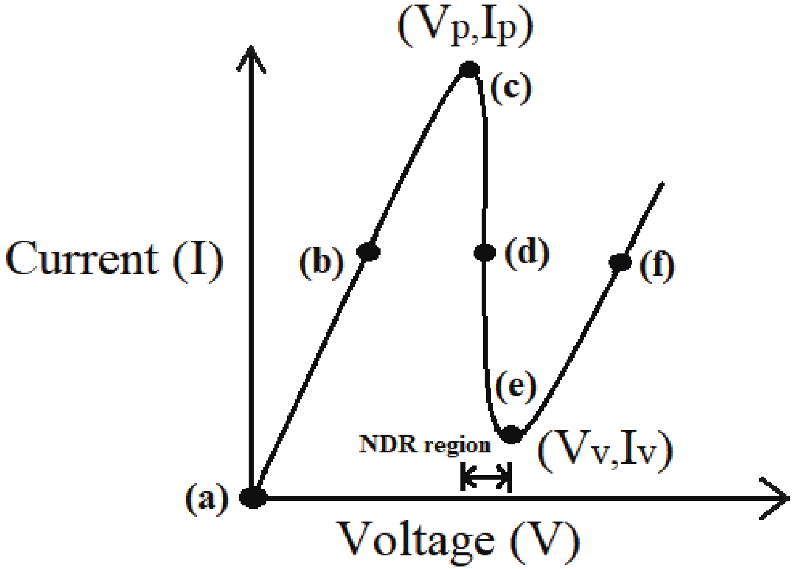
Fig. 2 Corresponding I–V characteristics of a typical double-barrier RTD structure.
Download figure:
Standard imageFrom Fig. 2, it can be seen that the current–voltage characteristics of an RTD are highly nonlinear, with a NDR region occurring at the peak current. This NDR region is due to the resonant tunneling mechanism, where a small change in the bias voltage can cause a large change in the current flowing through the device.
RTDs have been realized using various semiconductor materials and/or alloy systems, such as group IV (silicon (Si), silicon–germanium (Si–Ge)), and Ⅲ–V compound semiconductors (gallium arsenide (GaAs), indium phosphide (InP), gallium phosphide (GaP), gallium nitride (GaN)). These material systems differ in properties; thus, the choice of material plays a crucial role in the formation of good quality devices. Silicon-based devices are cheap, robust, and easy to process. However, due to their lower electron mobility, they operate more slowly than their Ⅲ–V counterparts. In addition, a wide band gap enables Ⅲ–V based devices to operate at higher temperatures and produce lower thermal noise at room temperature. A list of the properties of these material systems at room temperature[15, 16] is given in Table 1.
Table 1. Material properties for different semiconductors at room temperature.
| Material | Lattice constant (Ǻ) | Electron mobility (cm2/(V·s)) | Relative dielectric constant | Energy bandgap (eV) | Electron effective mass (m0) |
|---|---|---|---|---|---|
| Si | 5.43095 | 1500 | 11.9 | 1.12 (indirect) | l1: 0.98 t: 0.19 |
| Ge | 5.64613 | 3900 | 16.0 | 0.66 (indirect) | l: 1.64 t: 0.082 |
| GaAs | 5.6533 | 8500 | 13.1 | 1.424 (direct) | 0.063 |
| AlAs | 5.6605 | 180 | 10.1 | 2.36 (indirect) | 0.11 |
| Alx Ga1-x As | 5.6533 + 0.0078 x | 8 × 10³ – 2.2 × 10⁴ x + 104 x2 (for 0 < x < 0.45);–255 + 1160x – 720x2 (for 0.45 < x < 1) | 11.96 (when x = 0.33) | 1.42–2.36 (direct when x < 0.4) | 0.063 + 0.083x (for 0 < x < 0.45) |
| GaP | 5.4512 | 110 | 11.1 | 2.26 (indirect) | 0.82 |
| GaN | a = 3.189 c = 5.182 | 400 | 10.4 | 3.44 (direct) | 0.27 |
| InP | 5.8686 | 4600 | 12.6 | 1.35 (direct) | 0.077 |
Among the RTDs based on Ⅲ–V compound semiconductor material system, GaAs (direct bandgap material) heterostructures were found to be the most prevalent in the early days owing to its high electron mobility. These RTDs consist of a GaAs well sandwiched between AlAs or AlGaAs barriers. The advantage of using this material system is that AlAs and AlGaAs are lattice matched with GaAs, and thus have less material stress. However, the barrier height is low in this material system. This will result in high thermionic emission current, and as a result will be responsible for high valley current at room temperature. The electron effective mass for GaAs/AlGaAs RTDs is high, which reduces the current electron mobility and ultimately results in a decrease in current density. In addition, these RTDs suffer from low conduction band offset (as depicted in Fig. 3) which produces high leakage currents at the upper resonant level.
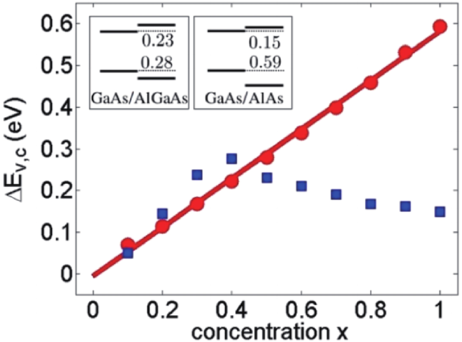
Fig. 3 (Color online) Conduction (blue square) and valence band (red dot) offsets for Alx Ga1−x As/GaAs interface with varying aluminum concentration. (Reprinted with permission from Ref. [17]. ©2013 American Institute of Physics.)
Download figure:
Standard imageThe experimental I–V characteristics of a double-barrier RTD structure were first observed in 1974[3] and were based on GaAs material technology. Since then, there has been extensive research on the technology, new material systems have been developed, and material growth has been used to obtain high quality RTD devices. Key technologies to obtain high quality RTDs include fabrication technology and structural design. Most of the reported material growth techniques to obtain high-precision ultrathin epi-layers use molecular beam epitaxy (MBE), while only a few use metal organic chemical vapor deposition (MOCVD). This is due to the fact that MBE is more precise and this gives more control of the deposited film thickness, alloy composition, and doping level[18−21].
In this review article, I will cover the development of GaAs RTD technology featuring significant accomplishments that have been achieved in terms of device design, fabrication, characterization, and applications to date. I will also give a research outlook on future developments with this technology. The organization of the article is as follows. Section 2 discusses different epi-structures used in GaAs-based RTDs, fabrication technology and device performances. Section 3 deals with the RTD applications. Finally, future perspectives and concluding remarks are given in Section 4.
2. RTD epi-structure: Device abrication and performance
The simplest RTD epi-structure consists of a quantum well sandwiched between double barriers: A top electrode and a bottom electrode[3]. The dimension of epitaxial layers including barrier thickness, quantum well, and spacer thickness needs to be varied to optimize the device performance, which depends on figure of merits, namely peak to valley current ratio (PVCR) and peak current density (Jp). To have a high PVCR, the peak current (Ip) needs to be as high as possible, while the valley current (Iv) should be as low as possible. However, if the peak current is too high, then it will cause high power dissipation. Consequently, a low peak voltage RTD needs to be designed in order to equilibrate this. Peak current density is inversely related to the barrier thickness—as barrier thickness decreases, it enlarges the transmission probability, which finally results in an increment of current density[22]. The distance between the adjacent resonant energy levels will increase if the quantum well is made narrow, so the leakage current components through the second resonant energy level will reduce, which ultimately enhances the PVCR[23−26]. The addition of a spacer layer in the RTD epi-structure prevents dopant diffusion to the subsequent layer in the growth process. However, a thick spacer layer widens the depletion region, which will affect high-frequency device performance by increasing the intrinsic delay time. It has also been found that introducing a spacer will result in an increase in the operating voltage. Furthermore, in specific designs, it has been shown that introducing doping in the active region can boost the performance of the device by altering the energy band structure and enhancing its current–voltage properties. In particular, doping can affect the tunneling current that flows through the RTD's active region[27−30].
High-frequency RTD device fabrication can be carried out by using one of the three processes, namely, a) Polyimide process[31], b) Air-bridge process[32, 33], and c) BCB (benzocyclobutene) process[34]. Processing steps in general involve sample cleaning, lithography, etching, and metallization. In the polyimide RTD process, the first fabrication step is the formation of top metal contact. Next is the top mesa step, which will etch till the emitter layer (using proper etching solution as depicted in Table 3). The bottom metal contact is deposited then following the same procedure as the top metal. The next step of fabrication is the bottom mesa, which etches till the substrate. This step isolates the active layers from the surrounding areas. The passivation step is done by using a polyimide (e.g., PI 2545), and thereafter the via-opening step is to be carried out in order to enable a connection between top contact and bond pads. Finally, metal bond pads are formed, which completes the single RTD device fabrication process. Figs. 4 and 5 show the RTD fabrication flow by using polyimide process and SEM (scanning electron microscope) image after fabrication, respectively.
Table 3. Wet etching solution for GaAs material around room temperature.
| Etching solution | Etchant ratio | Temperature (°C) | Etch rate (nm/min) | Ref. |
|---|---|---|---|---|
| NH4OH : H2O2 : H2O | 1 : 1 : 25 | 25 | 924 | [47] |
| 1 : 1 : 50 | 594 | |||
| 1 : 2 : 50 | 861 | |||
| 2 : 1 : 50 | 993 | |||
| 1 : 1 : 250 | 177 | |||
| 1 : 1 : 500 | 54 | |||
| 40 : 4 : 1 | Room temp. | 202.6 | [48] | |
| 40 : 10 : 0 | 509.1 | |||
| 40 : 20 : 0 | 1385 | |||
| 1 : 1 : 5 | 1890 | |||
| 1 : 10 : 500 | 25 | |||
| 10 : 1 : 500 | 18 | |||
| 1 : 10 : 5000 | 6.1 | |||
| 1 : 1 : 5000 | 1.65 | |||
| 1 : 10 : 3000 | 12 | |||
| HCl : H3PO4 : H2O | 1 : 10 : 1 | 20 | 10 | [49] |
| HCl : CH3COOH : H2O | 1 : 10 : 1 | 20 | 60 | [49] |
| HCl : CH3COOH : H2O2 | 1 : 20 : 0 | 20 | 10 | [50] |
| 1 : 20 : 1 | 50 | |||
| 1 : 20 : 2 | 120 | |||
| 1 : 20 : 3 | 270 | |||
| 1 : 2 : 1 | 440 | |||
| 1 : 5 : 1 | 250 | |||
| 1 : 10 : 1 | 120 | |||
| 1 : 20 : 1 | 50 | |||
| 1 : 30 : 1 | 30 | |||
| 1 : 40 : 1 | 15 | |||
| H3PO4 : H2O2 : H2O | 3 : 1 : 50 | Room temp. | 60 | [32] |
| 3 : 1 : 75 | Room temp. | 72 | [51] | |
| 1 : 1 : 25 | 25 | 259.8 | [47] | |
| 1 : 1 : 50 | 130.8 | |||
| 1 : 2 : 50 | 244.8 | |||
| 2 : 1 : 50 | 129 | |||
| 1 : 1 : 250 | 40.8 | |||
| 1 : 1 : 500 | 7.8 | |||
| H3PO4 : HNO3 | 3 : 1 | Room temp. | 1125 | [48] |
| H2SO4 : H2O2 | 4 : 1 | Room temp. | 1073 | [48] |
| H2SO4 : H2O2 : H2O | 4 : 3 : 3 | Room temp. | 9000 | [52] |
| 1 : 1 : 25 | 25 | 234 | [47] | |
| 1 : 1 : 50 | 90.6 | |||
| 1 : 2 : 50 | 202.8 | |||
| 2 : 1 : 50 | 184.8 | |||
| 1 : 1 : 250 | 27 | |||
| 1 : 1 : 500 | 27.6 | |||
| C6H8O7 : H2O2 | 2 : 1 | 20 | 30 | [53] |
| 3 : 1 | 45 | |||
| 4 : 1 | 45 | |||
| 5 : 1 | 42 | |||
| 7 : 1 | 33 | |||
| 10 : 1 | 21 | |||
| 1 : 1 | 18 | 5 | [54] | |
| 1 : 3 | 7 | |||
| 1 : 5 | 200 | |||
| 1 : 10 | 210 | |||
| 1 : 15 | 150 | |||
| 1 : 25 | 90 | |||
| 1 : 1 | 21 | 5.8 | [55] | |
| 2 : 1 | 570 | |||
| HCl : HNO3 | 3 : 1 | Room temp. | 477 | [48] |
| HCl : HNO3 : H2O | 1 : 1 : 1 | Room temp. | 2277 | [48] |
| HCl : H2O2 : H2O | 1 : 10 : 500 | Room temp. | 9.27 | [48] |
| 80 : 4 : 1 | 185 | |||
| 1 : 10 : 5000 | 8.21 | |||
| HF : HNO3 : H2O | 1 : 1 : 1 | Room temp. | 122693 | [48] |
Fig. 4 (Color online) RTD device fabrication flow by polyimide process: (a) top metal deposition; (b) top mesa; (c) bottom metal deposition; (d) bottom mesa; (e) passivation and via-opening; and (f) bond pad formation.
Download figure:
Standard image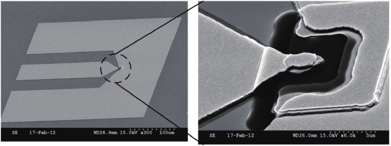
Fig. 5 SEM image of a fabricated RTD device with 3 × 3 μm2 mesa area. (Reprinted with permission from Ref. [31]. ©2014 University of Glasgow.)
Download figure:
Standard imageThe via-opening step, although crucial, is a critical process of RTD device fabrication, where a slight misalignment of mask and improper etch (underetch/overetch) may even result in device failure. In addition, creating a via-hole becomes very challenging when mesa size is of nanoscale dimension. This can be overcome with the air-bridge approach or by BCB process. RTD fabrication with air-bridge approach starts with top metal contact formation and mesa definition (which etches down to the emitter layer). Following this is a second etch step similar to the mesa step which results in a suspended air-bridge structure. Finally, there is bottom contact formation and bond pad establishment step. Thus, the air-bridge builds a connection between top metal and bond pad, thereby eliminating the critical via-opening step of polyimide process. The SEM image and actual micrograph of a GaAs/AlAs RTD device fabricated by the air-bridge process as reported by Zawawi[32] is shown in Fig. 6.
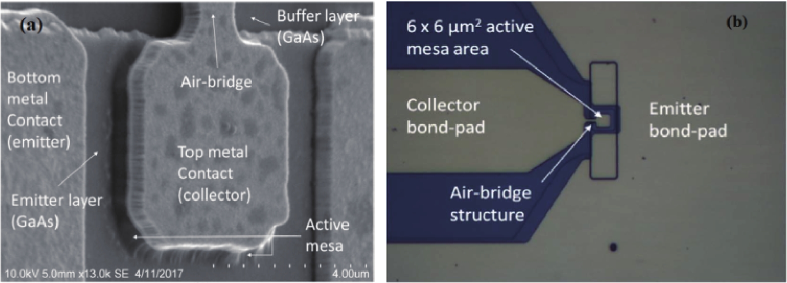
Fig. 6 (Color online) (a) SEM image and (b) actual micrograph of a GaAs/AlAs RTD device fabricated by air-bridge process. (Reprinted with permission from Ref. [32]. ©2017 Elsevier.)
Download figure:
Standard imageFabrication of RTD using BCB process starts with the top metal formation, top mesa, bottom metal formation, bottom mesa step, and passivation similar to the polyimide process. However, after this passivation, there is no via-opening. In this case, BCB etch back process to etch till top metal is undertaken and then bottom contact opening is done; finally, the bond pads are established. The cross-sectional view after the bond pad step is shown in Fig. 7.
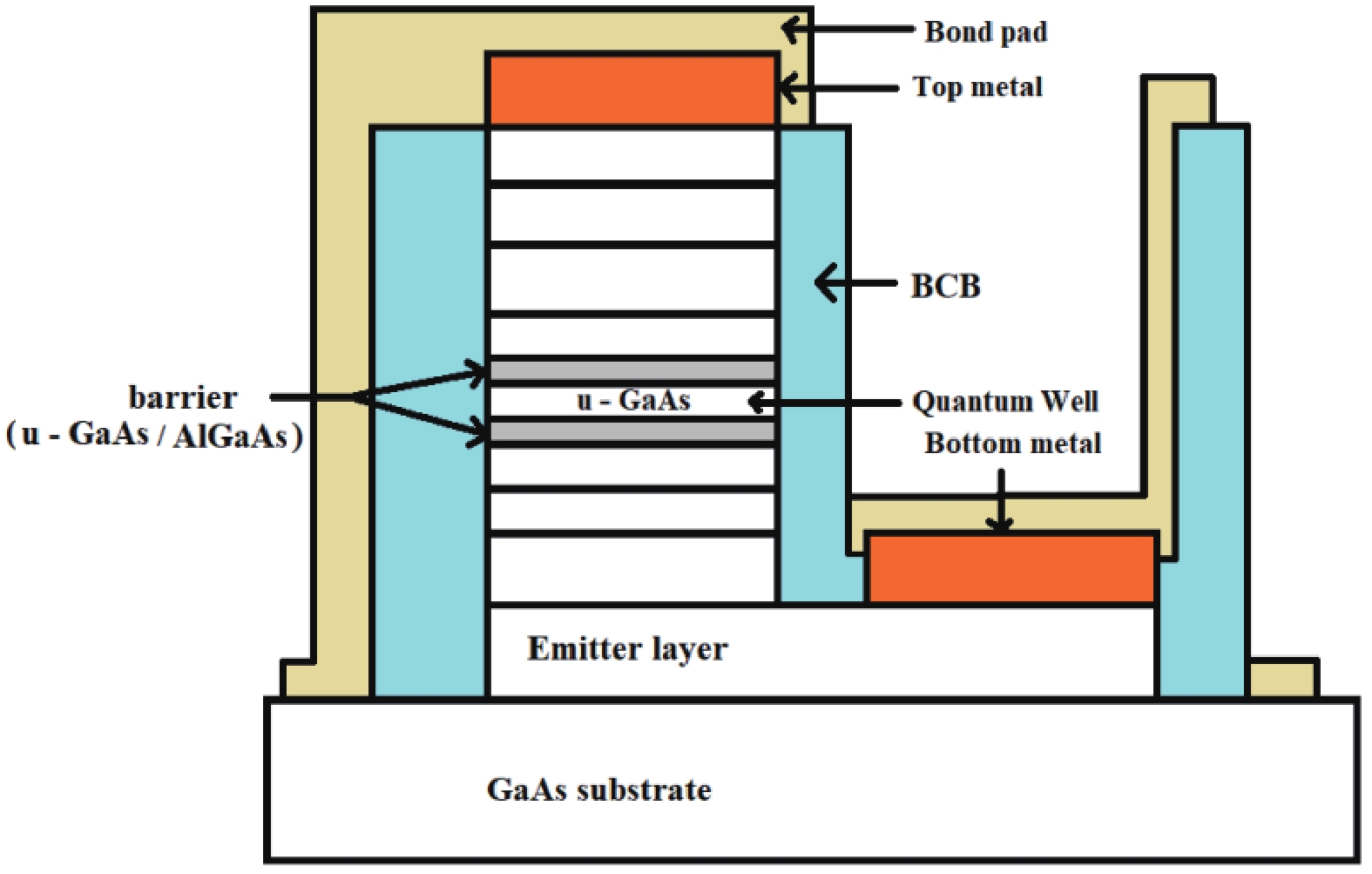
Fig. 7 (Color online) Cross section after bond pad establishment for BCB process of RTD fabrication.
Download figure:
Standard imageA suitable ohmic contact metallization scheme needs to be chosen for the fabrication of RTD, which will be thermally stable and have low contact resistance (Rc). These two are very important criteria for the performance and reliability of any semiconductor device, including the RTD. Ohmic contacts in general provide a link between external circuit and active regions of semiconductor devices. The choice of ohmic contact metallization becomes even more critical for devices with dimensions in the sub-micrometer range. Generally, ohmic contacts for GaAs are deposited by either evaporation or sputtering techniques, and the contact resistances are measured by using transmission line model (TLM). Table 2 shows the state-of-the-art methods and materials for obtaining ohmic contacts to GaAs.
Table 2. Ohmic contact formation on GaAs substrate.
| Metal scheme | Deposition method | Anneal temperature (°C) | Anneal time (s) | Specific contact resistance (Ω·cm2) | Ref. |
|---|---|---|---|---|---|
| Pd/Ge/Pd | EB-PVD | 430 | 15 | 3.2 × 10⁻⁴ | [35] |
| Pd/Ge/Ti/Pt | EB-PVD | 430 | 15 | 8 × 10⁻⁷ | [35] |
| Pd/Ge/Pd/Ti/Au | EB-PVD | 415 | 15 | 4.3 × 10⁻⁷ | [35] |
| Pd/Sn | Resistance-heating evaporation | 360 | 1800 | 3.26 × 10⁻⁵ | [36] |
| Pd/Ge/Ti/Au | EB-PVD | 340 | 20 | 2.8 × 10⁻⁶ | [37] |
| Pd/Ge/Ti/Pt | EB-PVD | 380–450 | 20 | (2.4–5.3) × 10–6 | [38] |
| Pd/Ge/Au/Pd/Au | EB-PVD | 400 | 30 | 2 × 10⁻⁶ | [39] |
| Pd/Ge/Au/Pd/Au | EB-PVD | 320 initially, then 400 | 20, then 60 | 2 × 10⁻⁶ | [40] |
| Au/Ge/Ni/Au | EB-PVD | 400 | 60 | 5.6 × 10⁻⁶ | [41] |
| Ge/Cu | EB-PVD | 400 | 1800 | 7 × 10⁻⁷ | [42] |
| Ge/Au/Ni/Ta/Au | Magnetron sputtering | 450 | – | 7 × 10⁻⁷ | [43] |
| WSi/Cu | RF sputtering | 400 | 5 | 6.3 × 10⁻⁶ | [44] |
| Au/Ti/W/Ti | Sputtering and EB-PVD | 400 | 30 | 5.5 × 10⁻⁶ | [45] |
| In | IAD | 375 | 60 | 3 × 10⁻⁶ | [46] |
Optical lithography using chrome/glass mask is the most commonly used approach to fabricate a GaAs-based RTD device. This method is inexpensive, and provides adequate resolution and high throughput when compared to the well-known maskless lithography technique—electron beam lithography. As device manufacturing using photolithography often requires wet etching, the next focus would be on the chemical wet etching solution. Etchant composition, concentration, and processing temperature are the crucial factors that affect the etching profile. Table 3 illustrates the state-of-the-art wet etchants for GaAs material around room temperature. The etchants are based on ammonium hydroxide, hydrochloric-based, sulfuric-based, orthophosphoric, or citric acid-based etching solutions. Although the wet etch method has the advantage of being low cost, it causes low damage to surface, and provides high selectivity, a dry etch method is also required where the main concern is to obtain high resolution and vertical sidewalls. Table 4 provides details of dry etching for GaAs material.
Table 4. Dry etching details for GaAs material.
| Inductively coupled plasma etching | ||||||
| Gas system | Flow rate (sccm) | RF power (W) | ICP power (W) | Chamber pressure (mTorr) | Etch rate (μm/min) | Ref. |
| BCl3/Cl2 | 30/80 | 80 | 600 | 10 | 2.6 | [56] |
| 800 | 4.5 | |||||
| 1000 | 5.4 | |||||
| 1200 | 6.2 | |||||
| 1500 | 6.4 | |||||
| 600 | 5 | 3.2 | ||||
| 10 | 2.8 | |||||
| 15 | 1.8 | |||||
| 20 | 1.2 | |||||
| 150 | 10 | 3.6 | ||||
| 200 | 4.0 | |||||
| 300 | 4.4 | |||||
| BCl3/Cl2 | 3 : 4 (ratio) | 90 | 950 | 40 | ~4.0 | [57] |
| BCl3/Cl2 | 4 : 1 | RF : ICP = 1 : 8 | 10 | 3.64 | [58] | |
| 2 : 1 | 3.6 | |||||
| 2.5 : 1 | 2.38 | |||||
| 6 : 1 | 2.37 | |||||
| 8 : 1 | 2.1 | |||||
| BCl3/Cl2/Ar | 4 : 1 : 5 | RF : ICP = 1 : 8 | 10 | 2.38 | [58] | |
| 2.5 : 1 : 5 | 2.13 | |||||
| 6 : 1 : 5 | 2.0 | |||||
| BCl3/Cl2/Ar/N2 | 6 : 1 : 5 : 2 | RF : ICP = 1 : 8 | 10 | 3.84 | [58] | |
| 6 : 1 : 5 : 2.5 | 4.0 | |||||
| 6 : 1 : 5 : 3 | 4.0 | |||||
| 3 : 1 : 5 : 3 | 2.5 | |||||
| 20 : 1 : 5 : 3 | 1.8 | |||||
| 5 | 1.14 | |||||
| 20 | 2.36 | |||||
| 25 | 3.6 | |||||
| 30 | 3.7 | |||||
| 20 : 1:5 : 5 | 30 | 5.56 | ||||
| 20 | 4.1 | |||||
| 20 : 1 : 10 : 3 | 20 | 2.8 | ||||
| 20 : 1 : 20 : 3 | 3.0 | |||||
| 20 : 1 : 30 : 3 | 2.5 | |||||
| 20 : 1 : 50 : 3 | 2.23 | |||||
| BCl3/Cl2/N2 | 20 : 1 : 3 | RF : ICP = 1 : 8 | 10 | 1.92 | [58] | |
| Cl2/Ar | 13/20 | 80 | 250 | 7.5 | 1.37 | [59] |
| 150 | 1.6 | |||||
| 200 | 1.82 | |||||
| Cl2/Ar/SiCl4 | 13/20/5 | 150 | 250 | 7.5 | 1.65 | |
| Reactive ion etching | ||||||
| Gas system | Flow rate (sccm) | RF power (W) | Chamber pressure (mTorr) | Etch rate (μm/min) | Ref. | |
| CCl4/CCl2F2 | 1/5 | 200 | 40 | 1.3 | [57] | |
| CCl2F2/He | 10/15 | 85 | 10 | 0.2 | [60] | |
| 20 | 0.5 | |||||
| 30 | 0.7 | |||||
| 40 | 1.05 | |||||
| 50 | 1.3 | |||||
| 60 | 1.4 | |||||
| SiCl4/Ar | 5/10 | 20 | 30 | 0.75 | [61] | |
| 30 | 1.25 | |||||
| 50 | 1.25 | |||||
| 30 | 50 | 1.5 | ||||
| 80 | 2.5 | |||||
| SF6/(BCl3 + SF6) | 1 : 5 | 150 | 50 | 1.8 | [62] | |
| 2 : 5 | 4.2 | |||||
| 11 : 20 | 5.5 | |||||
| 3 : 5 | 2.7 | |||||
| 4 : 5 | 4.5 | |||||
| CCl2F2/Ar | 1 : 10 | 200 | 200 | 0.32 | [33] | |
| 300 | 0.23 | |||||
| 400 | 0.15 | |||||
| 500 | 0.08 | |||||
| 600 | 0.15 | |||||
There are intense research efforts to optimize the performance of RTDs to be utilized as building blocks of electronics, as well as optical devices. Presently, fabrication demands maximum performance with minimum device size. However, scaling down device size increases the on-chip device density and decreases the capacitance, which ultimately lowers the cut-off operating frequency[63]. Table 5 shows the state-of-the-art performance of GaAs-based RTDs in terms of PVCR and peak current density at room temperature. Generally, a parameter analyzer is used to measure the RTD DC characteristics, where the bond pads are connected to the terminals on the parameter analyzer through two DC probes, and measurement software is used to manage measurement and enable data collection. It can be observed from Table 5 that a proper choice of material system, thereby adjusting the doping concentration of contact regions, will help to improve the performance of RTD structures. The dimensions of the individual layers forming the RTD device (i.e., barrier, well and spacer thicknesses) also play important role in performance improvement.
Table 5. Performance of GaAs-based RTDs at room temperature.
| Material system | PVCR | Jp (kA/cm2) | Mesa size | Ref. | |
|---|---|---|---|---|---|
| Barrier (nm) | Well (nm) | ||||
| AlAs (1.7) | GaAs (4.5) | 3.5 | 40 | − | [64] |
| Al0.3Ga0.7As (3.0) | GaAs (4.5) | 1.3 | 12 | − | [65] |
| AlAs (2.5) | GaAs (4.5) | 1.7 | 8 | − | |
| AlAs (1.5) | GaAs (4.5) | 3.5 | 40 | − | |
| AlAs (1.1) | GaAs (4.5) | 1.5 | 150 | Φ = 4 μm | [66] |
| Al0.3Ga0.7As (5.0) | GaAs (5.0) | 1.8 | 30 | 177 μm2 (Φ = 15 μm) | [67] |
| AlAs (1.7) | GaAs (5.0) | 4.1 ± 0.1 | 48.8 ± 3.8 | − | [68] |
| 3.8 ± 0.2 | 52.2 ± 2.2 | − | |||
| AlAs (1.7) | GaAs (4.5) | 2.0 | 160 | Φ = 3.5 μm | [69] |
| AlAs (1.4) | GaAs (5.1) | 1.8 | 250 ± 20 | (1−3) × 5 μm2 | [70] |
| AlAs (1.7) | GaAs (4.5) | 2.0 | 140 ± 10 | ||
| AlAs (1.4) | GaAs (4.5) | 1.7 | 200 ± 20 | ||
| AlAs (1.7) | GaAs (4.5) | 5.0 | 35 | 49 | [71] |
| AlAs (1.7) | GaAs (5.0) | 4.8 | 8.3 | 36 | [72] |
| AlAs (4.0) | GaAs (5.5) | 1.45 | − | 900 | [73] |
| AlAs (2.0) | GaAs (5.0) | 4.1 | 13.3 | 49 | [74] |
| 5.0 | 14.7 | ||||
| Al0.42Ga0.58As (5.0) | GaAs (5.0) | 3.9 | 0.61 | 520 | [75] |
| Al0.42Ga0.58As (1.7) | GaAs (5.0) | 5.35 | 40 | >16 | [76] |
| AlAs (1.7) | GaAs (4.0) | 2.9 | 6 | 100 | [77] |
| AlAs (4.0) | GaAs (4.7) | 2.9 | 2 | 2500 | [78] |
| 1.7 | 1.53 | 7500 | |||
| AlAs (1.7) | GaAs (4.5) | 3.5 | 100 | 12 | [79] |
| AlAs (1.96) | GaAs (5.0) | 4.0 | 20 | 75 | [80] |
| AlAs (1.7) | GaAs (6.5) | 3.27 | 14.8 | 16 | [32] |
| 3.44 | 15.93 | 25 | |||
| 3.38 | 14.8 | 36 | |||
3. Application
Resonant tunneling diodes exhibit a wide variety of applications in electronics and communication systems, including high-speed digital circuits, microwave oscillators, terahertz detectors, and optical applications (Table 6). The unique properties of RTDs, such as their high-frequency response and low power consumption, make them an attractive choice for these applications. RTDs are known to be the fastest semiconductor-based electronic devices to date[81, 82]. Tunneling time and device capacitance are very small in these devices, which makes their operation frequency and switching speed the fastest when compared to other semiconductor-based electronic devices, and are thus used in high-frequency electronics. With a higher peak current density, RTDs will have faster switching speed, provided that the PVCR is kept high and the device capacitance is kept low. RTD can potentially operate in the terahertz (THz) regime because it is only limited by tunneling time of the electrons, which is in the order of picoseconds. The NDR allows fast oscillations, so oscillators can be made that will oscillate at THz. This NDR also allows RTD to be applicable in digital logic circuits[83]. One can make the RTD oscillate at very high frequency with a small device capacitance and small intrinsic delay. In 1984, Sollner[84] reported the first demonstration of GaAs/AlGaAs RTD oscillator at an oscillation frequency of 18 GHz at 200 K temperature. Oscillators operating at room temperature were reported later by Brown[64−66] for GaAs/AlAs RTDs, and could work up to 420 GHz[66]. Operation of the RTD as both oscillator and detector is possible by changing the operation bias voltage, and therefore RTDs can be used in realization of compact and low-cost transceivers. Research has also been done for RTD photodetectors (PD) on GaAs substrates (GaAs/AlGaAs RTD PD) by the inclusion of quaternary absorption layer like GaInNAs, which is pseudomorphically grown on GaAs substrates[85]. In order to enable wavelength-selective detection and enhance the quantum efficiency, RTDs are often integrated with distributed Bragg reflector (DBR) cavity[86, 87]. Sensitivity and wavelength selectivity depends on the number of DBR mirror pairs used—increasing the mirror pairs enhances both sensitivity and wavelength selectivity. The detection efficiency can also be enhanced with integrated waveguide geometry, as reported by Pfenning[87], where the waveguide design was for a wavelength of 940 nm. Effort has also been made to make use of RTDs as pressure sensors[88], mixers[77], and in trigger circuits[79].
Table 6. Applications of GaAs-based RTDs.
| RTD as oscillator | |||||
|---|---|---|---|---|---|
| Material system | Operation frequency (GHz) | Temperature (K) | Output power (μW) | Ref. | |
| GaAs/AlGaAs | 18 | 200 | 0.5 | [84] | |
| GaAs/AlAs | 200 | 300 | 20 | [64] | |
| 60 | 60 | ||||
| 3 | 100 | ||||
| 0.2 | 200 | ||||
| GaAs/AlAs | 56 | 300 | 60 | [65] | |
| 87 | 18 | ||||
| GaAs/AlAs | 3 | 300 | 150 | [66] | |
| 12 | 150 | ||||
| 50 | 50 | ||||
| 100 | 25 | ||||
| 220 | 2 | ||||
| 350 | 0.2 | ||||
| 420 | 0.2 | ||||
| GaAs/AlGaAs | 2 to 12 | 300 | − | [67] | |
| GaAs/AlAs | 38.6 | 300 | 36 | [69] | |
| 110 | 12 | ||||
| RTD as photodetector/light sensor and in single photon detection | |||||
| Device scheme | Wavelength (μm) | Voltage (V) | Absorption (%) | Sensitivity (kA/W) | Ref. |
| RTD with absorption layer | 1.3 | 3.0 | − | 0.966 | [85] |
| RTD integrated into DBR cavity | 1.29 | 4.0 | 18.3 | 31.2 | [86] |
| RTD integrated into DBR cavity | 0.94 | − | 90 | − | [87] |
| Waveguide-integrated RTD | 0.94 | − | > 90 (max 99) | − | [87] |
| RTD as pressure sensor | |||||
| Material system | Frequency (kHz) | Sensitivity (kHz/MPa) | Ref. | ||
| GaAs/AlGaAs | 113 | 0.8 | [88] | ||
| RTD as switch | |||||
| Material system | Switching time (ps) | Voltage swing (mV) | Ref. | ||
| GaAs/AlAs | 20 | 60 | [80] | ||
| RTD as subharmonic mixer | |||||
| Material system | Threshold voltage for resonant tunneling (V) | Temperature (K) | Local oscillation power (dBm) | Conversion loss (dB) | Ref. |
| GaAs/AlAs | 0.75 | Room temp. | 12 | 11 | [77] |
| RTD in triggering | |||||
| Material system | Frequency range (GHz) | Time jitter (ps rms) rms) | Bandwidth (GHz) | Ref. | |
| GaAs/AlAs | 5 to 50 | <1 | 60 | [79] | |
4. Conclusions and future perspectives
RTDs have become a research focus due to their NDR current–voltage characteristics, structural simplicity, low fabrication cost, inherent high speed, design flexibility, versatile circuit functionality, and ability to operate at room temperature. NDR is the reason why RTDs have found potential for high-speed and high functionality operations, thus gaining the attention to researchers working in this field. Researchers and scientists from different parts of the world have been working with RTDs using GaAs material system to make them applicable for a wide range of applications. The advent of various advanced epitaxial growth techniques and fabrication methods makes it possible to improve the performance and allows them to be applied in many areas. However, there is much research space for the development of this GaAs RTD technology. In particular, much optimization is required to make it potential for real-world applications, especially in terahertz and neuromorphic applications. In recent years, there has been a trend of developing RTD devices in brain-inspired optical memories and neuromorphic computing. Neuromorphic electronic circuits that are based on optoelectronic devices are formed by RTDs to enable electro-optic neuromorphic functions. It is highly expected that in the near future the research focus would be on the implementation of neuromorphic applications using GaAs-based RTDs.