
Abstract
Buried-regrown-implant-structure (BRIS) technology combines two-step epitaxial regrowth with an intermediate ion implantation step in order to realise a buried current aperture close to the active region of a laser diode. In this paper we carry out a systematic performance comparison demonstrating the benefit of BRIS technology in single emitter broad-area lasers (BALs). We investigate stripe width W = 100 μm and resonator length L = 4 mm single emitter lasers emitting at wavelength λ = 915 nm, comparing the performance of BRIS devices with different implantation depths with reference devices with only contact layer implantation. We show that using BRIS technology we achieve a continuous wave output power of 20 W at 57% efficiency, with a peak efficiency of 68%, and maintain a lateral brightness of 3.4 mm · mrad up to 19 W, improved over the reference devices due to reduced lateral current spreading in the BRIS devices. Further, we show results of ongoing aging experiments, which has shown no device degradation up to 5000 hours from BRIS devices.
Export citation and abstract BibTeX RIS

Original content from this work may be used under the terms of the Creative Commons Attribution 4.0 licence. Any further distribution of this work must maintain attribution to the author(s) and the title of the work, journal citation and DOI.
1. Introduction
High-power broad area laser (BAL) diodes allow for the very high efficiency conversion of electrical energy to coherent optical energy and are a critical component for a variety of applications, either as direct sources or as pump sources. Whether being utilised in single emitter configurations, or as laser bars, a continual challenge for high-power BALs is increasing output power and beam quality, especially for fibre-coupling applications [1–3] as recently reviewed in [4]. For BALs we are generally concerned with the lateral beam quality of the laser, as typical edge emitters are diffraction limited in the vertical direction. Therefore, we can state this aim as increasing the lateral brightness of the laser, defined as:

where POpt
is optical output power and BPPLat
is the lateral beam parameter product defined as  where W95% is the 95% power content lateral near-field width and Θ95% is the 95% power content lateral far-field angle.
One long standing challenge in improving the lateral brightness of a BAL is managing the lateral current spreading in a device. In this, carriers are able to spread outside of the defined lateral stripe after current injection before they recombine in the active region. Current spreading can reduce lateral brightness by increasing the threshold current of the laser [5–7] which degrades efficiency and thermal performance, by reducing slope efficiency above threshold [8, 9], and through increasing BPPLat through associated far-field blooming mechanisms [10–12].
Recently, buried-regrown-implant-structure (BRIS) technology has been developed in order to restrict lateral current spreading in laser diodes. Using BRIS, ion implanted current blocking layers are formed close to the active region of the laser through the use of two-step epitaxial regrowth for improved performance with a variety of implant species [13, 14]. It was shown that BRIS can be used to realise a single-emitting laser which very thick epitaxial p-side layers, without penalty to efficiency or beam quality [15]. In this paper we will further analyse the benefits of this technology in stripe width W = 100 μ m single emitters emitting at wavelength λ = 915 nm focusing on oxygen implantation due to it's high stability. We investigate the benefit of the technology by considering devices with and without BRIS, and by varying the distance between the current blocking layers and the active region. It will be shown that using BRIS technology to move the current blocking regions closer to the active region of the device results to a small improvement in device efficiency, and a notable improvement in BPPLat . We will show through comparison to reference devices that these improvements are achieved by restricting lateral current spreading. Further, for we report aging experiments of oxygen-based BRIS devices and show that there is no device degradation up to 5000 hours of operation.
2. Technology and methods
A number of technologies have been demonstrated to restrict lateral current spreading in BALs, in the simplest case the highly doped p-contact layer is proton implanted or removed through etching in order to restrict spreading in this layer [16], however this allows for current to spread laterally between this layer and the active region. Technologies for blocking current spreading deeper in the p-side of structure include one-step epitaxy solutions such as deep ion implantation [12] and deep etched trenches [17]. There are also a number of suggested two-step epitaxy techniques such as the buried mesa laser in which the quantum well is etched outside the stripe [18]. A notable example is the recently developed enhanced self aligned lateral structure (eSAS) laser [19], a variant of previously demonstrated SAS designs [20, 21], in which buried current blocks are realised through two-step epitaxial regrowth with an in situ etching step to realise a structure with n-doped layers in the p-side of the device where current flow is desired to be blocked. The benefit of BRIS compared to these other methods are that it is not anticipated to introduce any additional index guiding which can degrade beam quality [12], and it is a completely planar process with no etching steps which can introduce potential defects or losses that degrade performance and reliability or induce index steps. Previous work also indicates that the use of BRIS does not necessarily introduce additional optical losses in the device if does not penetrate strongly into the active region [13], unlike high energy deep-implantation [12]. The current study seeks to optimise BLat by not introducing additional effects which can degrade POpt or BPPLat .
BRIS technology utilizes two-step epitaxial regrowth with an intermediate ion implantation step in order to realise a buried current aperture. In this method, the laser structure is grown from the n-substrate to the p-cladding layers, including the active region of the device. The wafers are then removed from the growth chamber, and implanted with 16O+ ions in regions in which current is to be blocked, with the implantation parameters controlling the depth and strength of the current blocking regions. After which the wafers are returned to the grown chamber where additional layers are grown to complete the vertical laser structure. In the regions which have been ion implanted, the oxygen has an insulating effect reducing the conductivity of the implanted layers [22]. Oxygen was used as the implantation species in this work as it is known to be thermally stable up to high temperatures [23–25], which is necessary as the wafer will reach high temperatures during the subsequent epitaxial regrowth. For further details of the mechanisms of the BRIS technology and the structure discussed in this paper see [13, 14].
In this paper we will compare four different device designs, which are summarised in table 1. Two of these device structures utilise BRIS technology for implementing buried current blocking layers, shown schematically in figure 1(a), while the other two use only contact implantation current blocks show in figure 1(b). For the BRIS lasers, the W = 100 μ m lateral stripe width is defined by the buried implantation, as current is blocked outside the stripe by the buried implantation. For the contact implantation laser the stripe width is defined by the width between the implantation in the p-contact layer after regrowth, below which injected carriers are able to spread outside of the stripe before reaching the active region. We note that the contact layer implantation in the BRIS devices with width W = 340 μ m is not required for device performance, it is used to isolate individual devices on a bar for on-wafer characterization prior to mounting. As this region is not exposed to high temperature regrowth, oxygen is not required and other implant species can be used (here, He+). The two BRIS device designs have been designed to realise different oxygen implantation profiles, which is expected to result in different dres values, the vertical distance between the end of the current blocking and the active region. These differences in implantation profile were achieved by changing the distance to the active region at the beginning of implantation, it is estimated as being ≈336 nm for 'BRIS-A' and ≈935 nm for 'BRIS-B', and using different energies to control the depth of the implantation. For the contact implantation devices, different dres values are achieved by varying the thickness of the p-side epitaxy (not shown in figure 2), increasing the thickness of the final p-GaAs layer from ≈700 nm in the 'Contact-A' devices to ≈2700 nm in the 'Contact-B' devices, as carried out in [15].
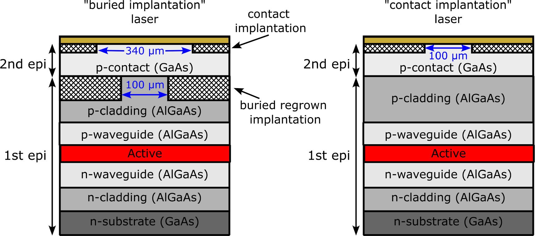
Figure 1. Schematic (not to scale) vertical cross section structure of a W = 100 μ m buried-regrown-implant-structure (BRIS) laser and a W = 100 μ m contact implantation laser.
Download figure:
Standard image High-resolution image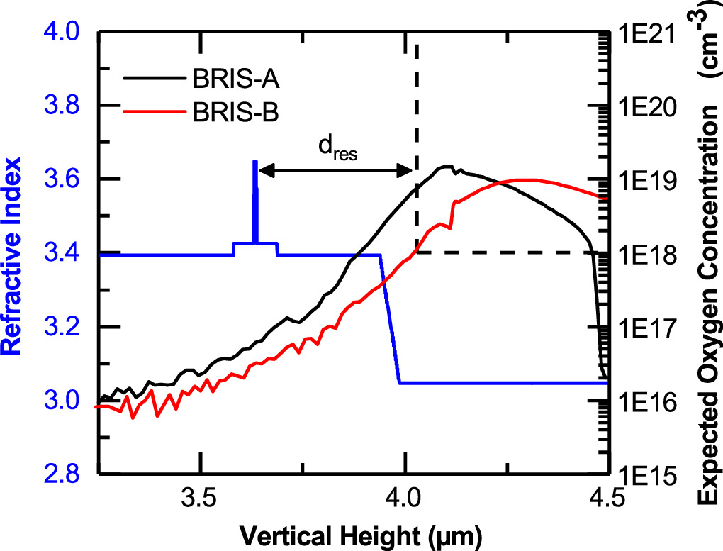
Figure 2. Estimated oxygen implantation concentration profiles of the two buried-implant varieties, as a function of the simulated refractive index of the laser structure (blue).
Download figure:
Standard image High-resolution imageTable 1. The four category of device types considered in this paper, with different implantation types and depths. dres is the estimated vertical distance between the end of the current blocking and the active region of the laser.
| Name | Implantation type | dres (nm) | Number of devices measured |
|---|---|---|---|
| BRIS-A | Buried + contact | 260 | 5 |
| BRIS-B | Buried + contact | 395 | 16 |
| Contact-A | Contact | 1790 | 8 |
| Contact-B | Contact | 3790 | 2 |
The expected oxygen concentration profiles of the 'BRIS-A' and 'BRIS-B' device types were obtained by secondary ion mass spectroscopy on fabricated test structures. For the final lasers, small changes were made to the implantation energy compared to these test structures in order to optimise the design. The expected profiles plotted in figure 2 are hence the SIMS measurement of the initial test structures, which have subsequently been shifted in vertical height-position in order to compensate for the change in implantation energy in the final structure [26]. We use the quantity dres to quantify the distance between the current blocking implantation and the active region of the device, taking the 1 × 1018 cm−3 as the nominal end value of the blocking. For the contact implantation devices, which have no buried implantation, dres is the distance between the active region and the p-contact layer which was He+ implanted. As we do not have exact implantation profiles for the real devices we measured, these dres values should be treated as nominal values, but the general trends between the depth of implantation and device behaviour will give insights into the effects and of current blocking. Lateral spreading of the implantation is estimated from simulation to be small [26], <0.5 μ m, and to not play an important role in device performance.
As can be seen in figure 2, the BRIS devices have been designed to be able to block current in the highly doped p-side cladding layers without introduce significant damage to the quantum well (<2 × 1016 cm−3 oxygen-level in quantum well). The two BRIS different designs allow us to study the benefit of a deeper implantation into the p-waveguide of the laser, and hence compare to the two contact implantation devices with different p-cladding thickness.
After first growth, ion implantation, and regrowth, test structures were fabricated in order to measure the strength of the current blocking. In these test structures, the BRIS two-step epitaxial regrowth was carried out and W = 200 μ m and L = 4 mm stripes were fully implanted over the entire area of the stripe, and a voltage was applied across the device and current measured. This is shown in figure 3, for 'BRIS-A' (red) and 'BRIS-B' (black) devices, and compared to a broad-area laser without any implantation. It can be seen that both BRIS implantation schemes offer substantial current blocking, with over three orders of magnitude of reduced current flow at 1.5 V for all devices measured compared to the standard broad-area laser.
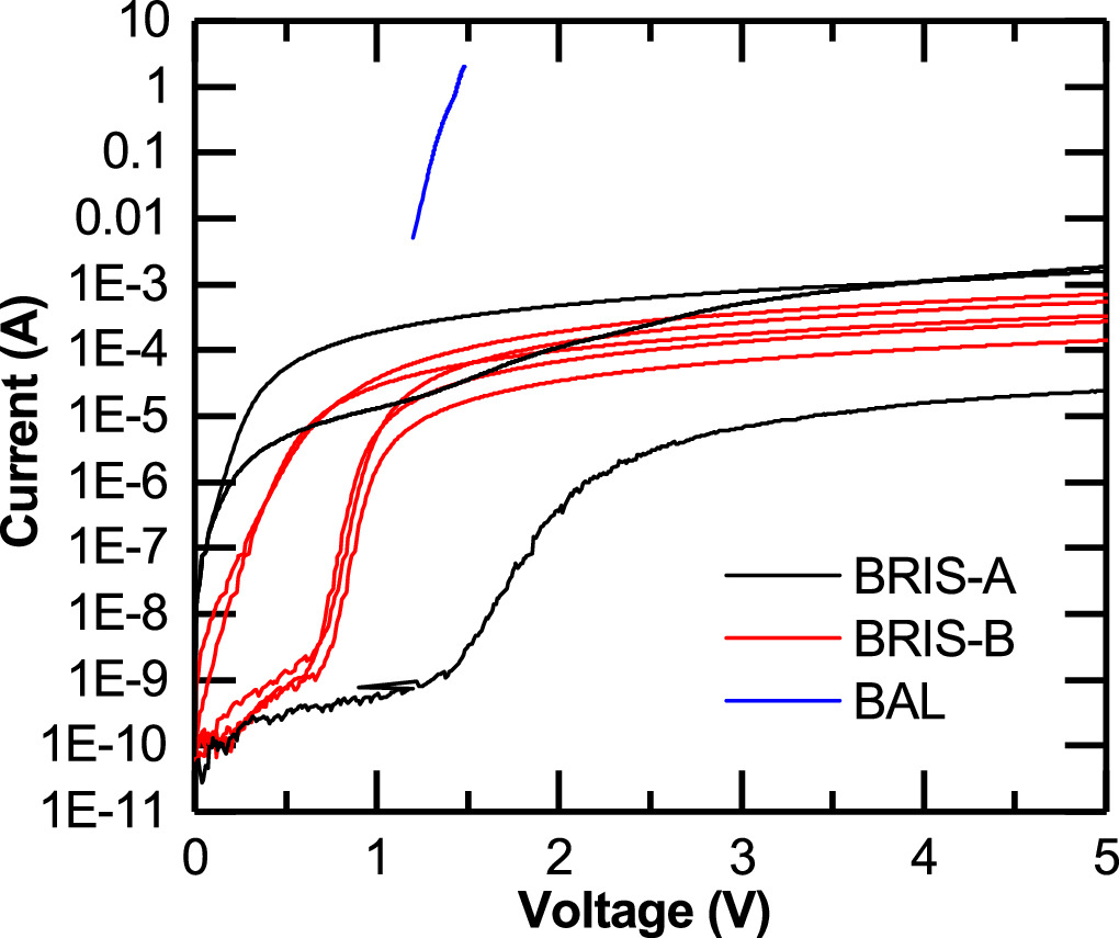
Figure 3. Measured current as a function of applied voltage for test structures with 'BRIS-A' and 'BRIS-B' type buried implantation, and a reference broad area laser (blue).
Download figure:
Standard image High-resolution imageIn this paper we consider single emitter laser diodes with resonator length L = 4 mm and lateral stripe width W = 100 μ m that make use of a vertically highly asymmetric epitaxial layer structure [27] emitting at λ = 915 nm, as discussed in [13, 14]. This epitaxial structure has been optimised for high power, high efficiency, continuous wave operation in single emitters. The lasers were cleaved, passivated, and coated for front facet reflectivity Rf = 1.8% and rear facet reflectivity Rr = 98%, and mounted p-side down on a passive CuW submount.
3. Results and discussion
3.1. Optical power, voltage, and efficiency
All of the devices were measured under continuous wave (CW) operation at a heatsink temperature of THS = 25 °C up to 12 A to determined the voltage, power, and power conversion efficiency characteristics of the devices, the power was measured using a calibrated thermoelectric detector. The best performing devices of each type were then measured up to high-power and the light-current-voltage (LIV) characteristics of these devices are shown in figure 4. It should be noted that during these measurements, none of the measured devices failed or completely thermally rolled over, the power was instead limited by the cooling capacity of the measurement station. It can be seen from this plot that all of the measured devices demonstrate very high-efficiency, high-output power operation, with every device reaching Popt = 20W with a power conversion efficiency ηe > 57%.
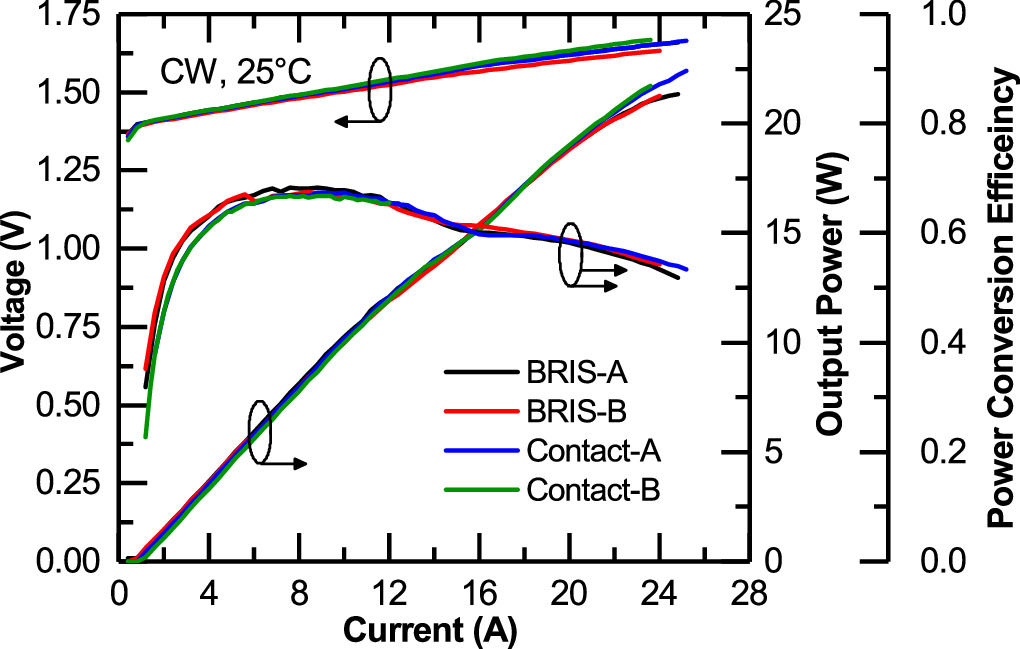
Figure 4. Continuous wave voltage, power, and power conversion efficiency at THS = 25 °C as a function of drive current for W = 100 μ m single emitters with varying implantation types.
Download figure:
Standard image High-resolution imageTo more clearly see the differences in the different device types we plot threshold current, slope efficiency, and peak power conversion efficiency as a function of dres for CW operation and THS = 25 °C. All devices in table 1 have been measured and averaged for these plots, with the error bars displaying the standard error of the mean. We note that the 'Contact-B' devices generally have a larger standard error, due to the smaller number of devices in this subset. It can be seen in figure 5(a) that as dres is reduced, the threshold current of the device is reduced generally. The two BRIS devices (black) are within the standard error of each other, Ith = 689 ± 5 mA and Ith = 680 ± 16 mA for BRIS − A and BRIS − B respectively, with no clear benefit to having a slightly deeper implantation for reducing threshold further. These results are in agreement with what we would expect to happen if we successfully block current spreading to outside of the lateral stripe, this then reduces the carriers spreading outside the stripe and reduces the current injection needed to reach the threshold gain condition.
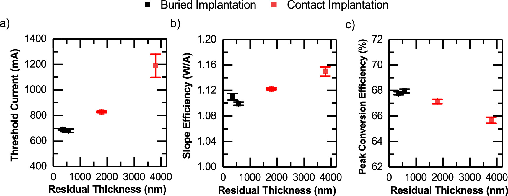
Figure 5. Continuous wave (a) threshold current, (b) slope efficiency up to 6 A, and (c) peak power conversion efficiency of W = 100 μ m single emitters as a function of residual thickness (dres ), at at THS = 25 °C.
Download figure:
Standard image High-resolution imageIn figure 5(b) we then consider the slope efficiency of the devices, which is measured from threshold up to 6 A for all devices. It can be seen that slope generally follows a comparable trend compared to threshold current, in that the slope efficiency of the devices is decreasing as we decrease dres . It is not clear why decreasing dres leads to a reduction in slope efficiency, it has been suggested that reducing lateral current spreading to outside the laser stripe should lead in an increase in slope [8], as this reduces the number of carriers that spontaneously recombine outside the laser stripe. However in this work, and in other recent work on reducing lateral current spreading [19] this is not generally observed. We believe that the reduced slope efficiency is not due to increased non-radiative losses due to the oxygen implantation, as this would not explain the difference in slope between the 'Contact-A' and 'Contact-B' device types, which do not include any buried implantation.
Finally, in figure 5(c) we plot the peak power conversion efficiency of the devices. It can be seen that as we reduce dres we seen an increase in peak efficiency. We should note that in the LIV plots in figure 4 the BRIS devices have a slightly worse output power at the highest currents (I > 20 A), we attribute this to the fact that under CW conditions the devices with reduced current spreading will suffer more from self-heating inside the stripe leading to a quicker onset of thermal rollover. The power and efficiency characteristics of these devices is comparable to the other high performance devices in the literature with W = 90...120 μ m, with the peak efficiency of η = 67.8 ± 0.1% and η = 68.0 ± 0.2% across the 'BRIS-A' and 'BRIS-B' devices respectively, and high efficiency of η > 57% at POpt = 20 W in all devices measured to high power.
In order to confirm that performance of BRIS devices is related to reduced current spreading, the amplified spontaneous emission (ASE) profile from the front facet of the device was measured for all devices below threshold (at current I ≈ 0.9*Ith ). These ASE profiles are shown in figure 6, with the expected position of the stripe edges marked with the black vertical dashed line. It can clearly be seen that the devices with contact implantation only have a larger fraction of spontaneous emission outside of the laser stripe, with the 'Contact-B' device, with the largest dres , having 46% of ASE within the stripe, compared to 52% for the 'Contact-A' device. Both of the buried implant devices have an increased fraction of ASE within the stripe, 57% for 'BRIS-A' and 59% for 'BRIS-B'. These results are consistent with the threshold current behavior shown in figure 5(a).

Figure 6. Amplified spontaneous emission profile imaged from front facet of the different device types at I = 0.9 ∗ Ith at THS = 25 °C. Vertical dashed lines indicate the W = 100 μ m stripe edges.
Download figure:
Standard image High-resolution imageA subset of these devices were then used in aging experiments in order to characterise the effects of the BRIS technology on device reliability. Five devices of 'BRIS-B' and five devices of 'Contact-B' were used in these aging experiments. The results so far are plotted in figure 7, plotting the normalised output power against the aging time under CW and THS = 25 °C conditions. All of the devices were age at a constant operating current which corresponds to a POpt = 10 W at the start of life. At 5000 hours of continuous operation there were no device failures, including the BRIS devices, and no measurable degradation in performance.
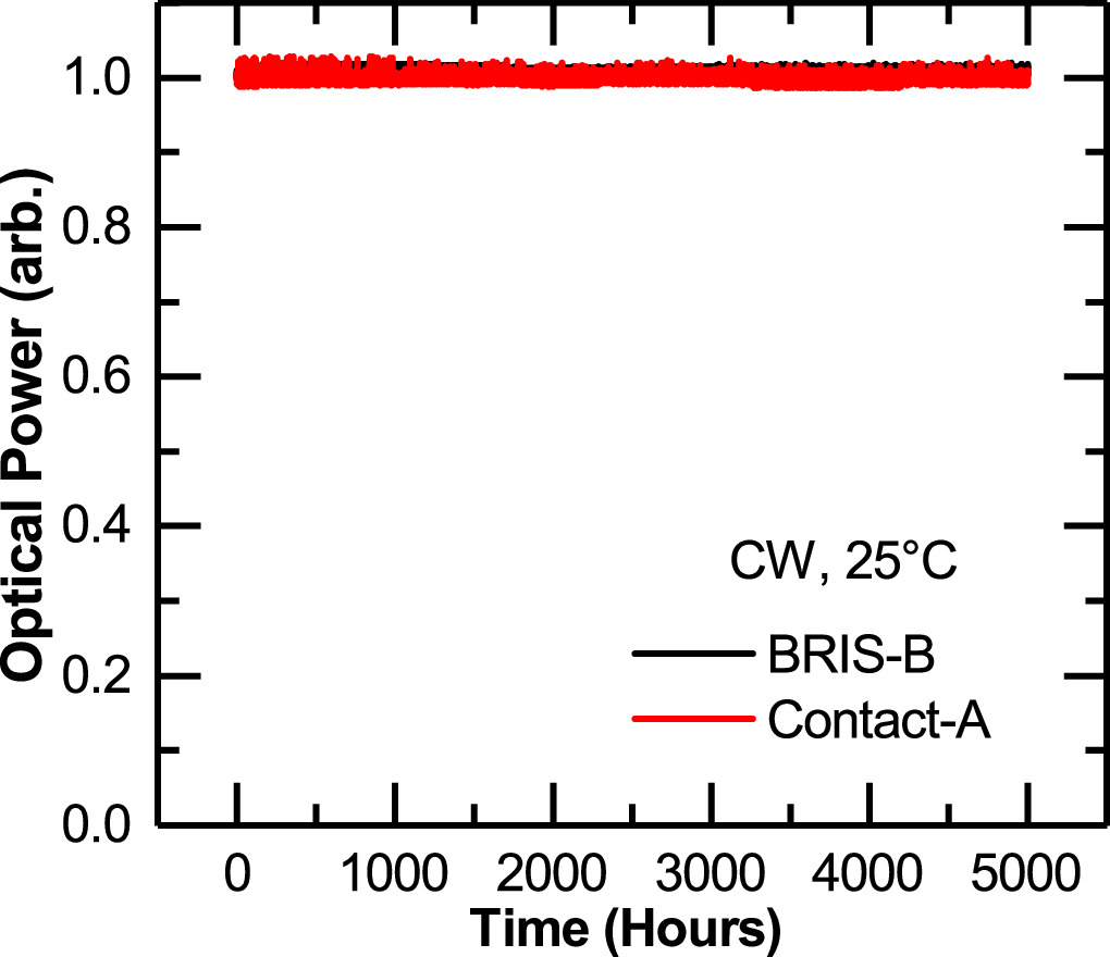
Figure 7. Constant current, continuous wave aging of W = 100 μ m single emitters for 5000 hours, measuring normalised output power as a function of time. Five 'BRIS-B' buried implant devices were aged and five reference 'Contact-A' devices. Constant current was chosen to correspond to Popt = 10W at the start of aging.
Download figure:
Standard image High-resolution image3.2. Beam quality measurement
The impact of BRIS designs on beam quality was next assessed, under CW conditions at THS = 25 °C as in the power measurements. For the beam-quality measurements the lateral near-field profile and the far-field profile of exemplary devices was measured up to POpt = 19 W. The profiles were measured using a telescopic arrangement, as described in [17]. In figure 8 the near and far-field profiles are plotted for all device types for a range of optical powers.
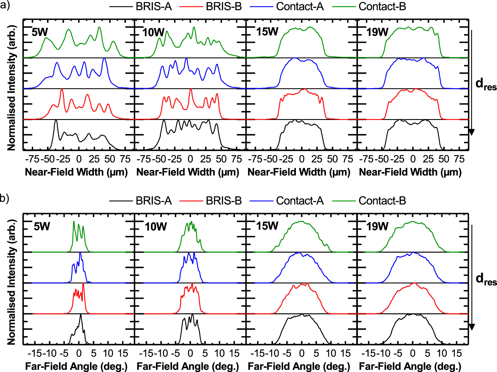
Figure 8. Continuous wave vertically integrated optical intensity as a function of (a) lateral position (lateral near-field profile) and (b) angle (lateral far-field profile) in the plane of the active region at THS = 25 °C. For each device type the near- and far-field profile is shown for Popt = 5W, 10W, 15W, 20W.
Download figure:
Standard image High-resolution imageIn figure 9 (a) the 95% power content near-field width, W95% of the four device types are plotted, and in b) the 95% power content far-field profile, Θ95% as a function of optical output power. It can be seen that for Popt < 12.5W there are clear differences in the near-field width between the device types. For the BRIS devices the near-field is generally much closer to the defined W = 100 μ m stripe, while the contact implantation devices are 10-30 μ m broader, with the thick p-side Contact-B device having the broadest near-field. 'BRIS-A' with the smallest dres generally has the smallest width, but it is similar to 'BRIS-B'. Through inspection of the near-field profiles in figure 8 (a) at Popt = 5W and Popt = 10W, the narrower near-field in this BRIS devices can be clearly seen. It can also be seen that the edges of the BRIS device near-field profiles are sharper than the contact implantation devices, in which the intensity decays slowly outside of the stripe, which can be attributed to moving the current aperture close to the active region. For Popt < 12.5W the far-field angle of all of the devices is generally comparable, with all devices displaying an angle of less than 8° at 10 W. No clear differences between the devices can be seen in the far-field profiles at these output powers.

Figure 9. Continuous wave beam-quality measurement of W = 100 μ m single emitters as a function of output power plotting (a) 95% power content lateral near-field width, (b) 95% power content lateral far-field angle, and (c) lateral brightness, and d) 95% power content lateral beam parameter product as a function of the increase in active zone temperature. THS = 25 °C.
Download figure:
Standard image High-resolution image
For Popt > 12.5W all of the near-field widths of the devices narrow to much smaller than W95% = 100 μ m, and inspection of the near-field profiles show no clear differences between the device types. This near-field narrowing is a known effect in the CW operation of broad-area lasers, where the near field profile of the device narrows at high power due to strong thermal lensing, which is exaggerated at the front facet by a varying longitudinal temperature profile in the device due to asymmetric facet reflectivities [28–30]. As the output power of the devices is increased, it can be seen that far-field angle of all devices increases, which occurs in BALs due to a combination of bias and temperature related effects. For Popt > 12.5W all of the devices display considerable far-field blooming consistent with the narrowed near-field, but with contact implantation devices having wider far-field angles than the BRIS devices. This can be seen by inspecting the far-field profiles of the devices at Popt = 15W and Popt = 19W, suggesting that through use of BRIS the lasing of some higher order modes has been restricted leading to a narrower far-field profile.
In figure 9(c) these results are summarised by plotting BLat as a function of output power. It can clearly be seen that over the range of powers measured there are clear benefits to BRIS technology for improved brightness. Both BRIS devices achieve BLat = 3.5 W/mm · mrad at Popt = 10 W, and maintain BLat = 3.4 W/mm · mrad up to Popt = 19 W of output. This is a clear improvement over both the contact implantation devices, in particular we see that 'Contact-B' with the thick p-side epitaxy and largest dres which has a large penalty to device brightness by moving the current aperture further away. These BLat values are comparable or an improvement to best reported highly efficient W = 90...120μ m devices in the literature, such as BLat = 3.3 W/mm · mrad at Popt = 12.5 W [31] and BLat ≈ 3.5 W/mm · mrad at 10 W [32, 33], but through the use of BRIS we are able to maintain achieve this brightness at ≈2 × higher output powers than previously reported. For Popt < 12.5W it can be seen that primarily the benefit to brightness in BRIS devices is due to the narrower near-field profile, while maintaining a comparable far-field angle. This can likely be attributed to the BRIS devices restricting the lasing of higher-order lateral modes compared to the contact implantation devices due to the narrower gain profile. For Popt > 12.5W it is a combination of a narrow near-field and reduced far-field angle compared to the contact implantation devices which leads to the improved brightness in the BRIS devices. It is not necessarily clear why at these high-powers the BRIS devices has narrower far-field, we suggest that it is possible due to current spreading leading to the large carrier accumulation at the stripe edges in these devices [34], increasing the gain available for the lasing of higher order modes as proposed in [17].
In figure 9 (d), following [4, 17] we plot the 95% power content BPPLat as a function of the change in active zone temperature, ΔTAZ , which indicates how the beam-quality of the device varies a function of generated heat. The change in active zone temperature is determined from the shift in central wavelength of the emission spectra [17]. We make a linear fit to the data for the different devices types, as has been carried out in previous studies [17, 19, 35], and apply the simple empirical formula BPPLat = BPP0 + Sth · ΔTAZ , where BPP0 is the temperature independent background contribution to the lateral beam quality and Sth quantifies the effects of bias and temperature dependent effects. Compared to the thick p-side 'Contact-B' device (Sth = 0.18 mm · mrad/K, BPP0 = 1.78 mm · mrad) the use of buried implantation has reduced both Sth and BPP0 for 'BRIS-A' (Sth = 0.15 mm · mrad/K, BPP0 = 1.46 mm · mrad) and 'BRIS-B' (Sth = 0.16 mm · mrad/K, BPP0 = 1.40 mm · mrad), indicating that reducing current spreading has improved the thermal and bias contributions to reduced beam-quality, as well as the background contributions, consistent with previous studies.
4. Summary
We have reported progress in improving the brightness and efficiency of BALs through reducing lateral current spreading. We demonstrate that through the use of BRIS technology, in which a buried current aperture is formed close to the active region of the device through two-step epitaxial regrowth and an intermediate ion implantation step that the beam quality of W = 100 μ m stripe lasers can improved, for no penalty to device efficiency. We demonstrated that a BRIS device could achieve a CW output power of Popt = 20W at 57% efficiency, improved ≈5% compared to previous studies [19]. The peak efficiency of the best performing configuration was measured to be η = 68.0 ± 0.2% over a range of devices, improved over reference devices. Further, the BRIS devices maintained a lateral brightness of BLat > 3.4 W/mm · mrad up to Popt = 19 W, which is approximately two times higher power than previously reported at this BLat . We demonstrated that these improvements correlated to reduced lateral current spreading in the device through comparison with contact implantation test structure with different p-side epitaxial thickness. Efficiency improvements were related to the reduced threshold in the devices. No clear performance benefit was seen by changing the implantation profile of the BRIS devices. An open topic is the relation between current spreading and slope efficiency, which was predicted in earlier work to increase, but here reduces as current spreading is suppressed.
Acknowledgments
The authors thanks H Wenzel (FBH) for providing the epitaxial structure used in this work. We thank the BMBF for funding within the European Union Eurostars Project, BRISCL, under contract number: 01QE2103D.
Data availability statement
The data cannot be made publicly available upon publication because the cost of preparing, depositing and hosting the data would be prohibitive within the terms of this research project. The data that support the findings of this study are available upon reasonable request from the authors.