
Abstract
This study aims to develop a multiscale bridging method for investigating nanocrystalline metals based on macro-scale deformation. For this purpose, we propose a hierarchical multiscale computational method that can focus on some of the elements in a finite element model for scale bridging to atomistic-scale models. This method assumes that atomistic-scale nanocrystalline models are related to the integration points in a finite element and deform based on the macro-scale deformation. Nanocrystalline aluminum was chosen for the validation of the multiscale method. The finite element method (FEM) and the molecular dynamics (MD) method were used for continuum-scale and atomistic-scale simulations, respectively. We utilized the notion of the CauchyBorn rule (CBR) for communicating deformation information from the continuum scale to the atomistic scale. We studied three different cases with two nanocrystalline models and two loading cases to compare differences resulting from crystal structures and loading. Based on the crystal structure change during relaxation, nonequilibrium grain boundaries (NEGBs) were shown to play a role as deformation mechanisms in the plastic regime and induce the onset and migration of crystal defects, including deformation twins, as reported in the experiment. Furthermore, the crystal orientation dependence of the onset of crystal defects was confirmed by the comparison of the results from the two different nanocrystalline models. The qualitative agreement of the results with experimental observations is also confirmed. The proposed 'FEM-MD' method can bridge a large-scale gap, for example, from a nano-scale to a continuum-scale such that an MD model can be coupled to a millimeter or centimeter scale compared to other embedding methods. The present method is ideal for investigating the dislocation behavior of nanocrystalline materials, which contain multi-grained nanostructure at finite temperature, undergoing various loading scenarios at the macro-scale.
Export citation and abstract BibTeX RIS

Original content from this work may be used under the terms of the Creative Commons Attribution 4.0 licence. Any further distribution of this work must maintain attribution to the author(s) and the title of the work, journal citation and DOI.
1. Introduction
Reducing the weight of metallic structural components has been advanced to deal with worldwide issues such as energy, environment, and resource depletion. To lighten structural components, it is essential to increase the strength of a material used in the structure. For this reason, many researchers have investigated strengthening mechanisms for metallic materials. The well-known strengthening techniques utilized for metals are dislocation hardening, hardening by grain refinement, solid-solution hardening, and precipitation hardening. Among these techniques, grain refinement strengthening has attracted much attention since it is a promising candidate that can simultaneously achieve high strength and high ductility [1]. In particular, metallic materials with a mean grain size from 1 nm to 100 nm are generally called nanocrystalline metals. Typical nanocrystalline metals are aluminum, copper, or nickel. The deformation mechanism of metallic materials with nano-scale grain sizes produced by grain refinement differs from that of conventional grain sizes. Notably, the stacking fault and the deformation twinning play a significant role in plastic deformation in nanocrystalline metals, contributing to high ductility [2–5].
Theoretical models of nanocrystalline materials that can account for the generation of deformation twinning, the migration of grain boundaries driven by stress, and the crack growth due to special rotational deformation have been proposed [6–8]. From the perspective of numerical analysis, the molecular dynamics (MD) method has been used to investigate the deformation mechanisms and mechanical properties. This is due to its capability of directly resolving nanocrystalline metals at the atomistic scale while using appropriate boundary conditions and interatomic potentials. The results of MD simulations have shown the formation of complex twinning networks due to dislocation interactions and dislocation-twin boundary reactions [9]. It has also been observed that the onset of deformation twinning is accompanied by the emission of partial dislocations from grain boundaries [10]. From the viewpoint of orientation dependence, those simulations have confirmed the tendency of the nucleation of twinning in specific directions [11, 12]. The studies focusing on the crystal grain size have reported that the grain size of nanocrystalline metals affects the mechanical properties such as hardness and yield strength [13, 14]. The MD investigation of nanocrystalline copper in terms of the nano-scratching rate observed that the plastic deformation induced by the scratching is determined by the dislocation-grain boundary interaction [15]. The simulation of nanocrystalline copper subjected to shock loading confirmed that the amount of the body-centered cubic structure depends on a specific grain orientation and a particle velocity assigned to each atom [16].
MD simulations of nanocrystalline metals have contributed significantly to the elucidation of the mechanisms and the understanding of their behavior. However, the size of MD computational models of nanocrystalline materials is limited to nano-scale due to their high computational costs. This problem makes it challenging to investigate the macroscopic mechanical properties of nanocrystalline metals using the MD method. To address this issue, multiscale computational methods have been developed. Multiscale simulations are computationally efficient ways to study macroscopic properties. Besides, multiscale concepts are deeply rooted in materials physics since most physical phenomena occur across different time and length scales. Multiscale simulations of nanocrystalline materials have been widely conducted over the last decade. One of the standard multiscale computational methods applied to materials with heterogeneous microstructures such as polycrystalline or nanocrystalline metals is the homogenization method [17–21]. In particular, the homogenization method has been utilized to investigate the material properties of materials with periodic microstructures such as composites [22] and porous metals [23]. When it comes to crystalline, some studies have performed numerical investigation using the homogenization method by exploiting a finite element microstructural representative volume element to account for the material responses of polycrystalline or nanocrystalline if nanoscale is assumed [24, 25].
Some other multiscale studies have employed a crystal plasticity model to take into account the generation and the glide of dislocations in the grain interior and have shown the capability of capturing typical characteristic phenomena of nanocrystalline metals, such as the inverse Hall-Petch effect or predicting damage and fracture [26–28]. The multiscale constitutive model that uses plastic energy dissipation to identify parameters related to microscopic phenomena showed good agreement with experimental data [29]. Moreover, another popular approach is the quasicontinuum method [30], which incorporates interatomic interaction into a finite element model by conducting crystal calculations based on the local deformation state. The results of the quasicontinuum simulations have shown a good ability to predict the plasticity and fracture in nanocrystalline materials [31–34]. Other types of atomistic-continuum modeling approaches have also contributed to a deeper understanding of the deformation mechanisms and their relation to the macroscopic properties [35, 36]. As an alternative, hierarchical multiscale methods, which are the focus of this paper, have emerged recently to efficiently model the macroscale deformation behavior of materials based on atomistic simulations. For example, a cohesive multiscale model that takes interatomic potential into account showed that the model could reproduce essential material properties such as fracture toughness and Young's modulus in single crystal silicon thin film by using the hierarchical CauchyBorn rule (CBR) [37]. Some studies have indeed utilized the higher-order CBR to take inhomogeneous deformation in crystalline materials into account [38, 39]. One of the examples is the incorporation of the higher-order CBR to develop an atomistic-informed crystal plasticity theory, where complex dislocation behavior and fracture of carbon nanotubes are considered [40, 41]. A similar case is an atomistic-informed continuum approach that succeeded in reproducing the macroscopic inelastic deformation and generation of shear bands in amorphous materials without phenomenological constitutive laws [42].
The present study is aimed at developing a multiscale method that hierarchically couples a continuum macroscale finite element model to an atomistic scale nanocrystalline model using the finite element method (FEM) and the Large-scale Atomic/Molecular Massively Parallel Simulator (LAMMPS) [43]. Based on the multiscale computation algorithm proposed by the authors for modeling amorphous polymers [44], here we develop a new multiscale method suited for nanocrystalline materials. In this method, atomistic-scale models are assigned to the integration points (IPs) of a finite element model and deform based on the macro-scale deformation history based on the classical CBR. The present method replaces fine-scale models with atomistic models, similar to the homogenization method referred to as FE2. In this sense, the method can be called a "FEM-MD" method. The FEM-MD method has an advantage in the application to the materials whose constitutive laws at a continuum scale are not well developed. Nanocrystalline metals are a class of materials that can be addressed using the FEM-MD method, given that the deformation mechanisms are primarily based on nano-scale interactions around grain boundaries. Nanocrystalline aluminum is considered in this study to demonstrate the applicability of the developed multiscale method to polycrystalline samples. The main difference between other atomistic-continuum bridging methods [45, 46] and the proposed FEM-MD is that in the scale bridging methods, an MD model is usually directly embedded in a continuum domain, coupled by a specially designed transition layer. Contrary to that, in the proposed FEM-MD method, the scales are not embedded but are coupled through the strain-stress response. Therefore, one of the advantageous features of the FEM-MD method is that it allows for bridging a much larger scale gap compared to other embedding methods. For example, coupling a nano-meter size MD model to a mm-size continuum model, which spans several orders of magnitude differences in length scale, is possible. Furthermore, the present method allows observation of dislocation behavior, including the onset and growth of stacking faults and deformation twins, in nanocrystalline materials resulting from a coarse-scale non-uniform sample shape change, which other methods have not showcased well.
This paper is comprised of five sections. In section 1, the background and the purpose of this study were described. Sections 2 and 3 are devoted to the introduction of the methods used in the simulation, i.e., MD, FEM, and the multiscale bridging algorithm, respectively. In section 4, the modeling setup is explained in detail. The results and the discussion on numerical examples are described following the modeling setup. Lastly, section 5 concludes the paper with some remarks.
2. Molecular dynamics simulation for nanocrystalline metallic materials and finite element method
In this section, the evaluation methods of interatomic potential function and stress, which are critical in MD simulations of nanocrystalline metals, are briefly explained. The formulation of the finite element method relevant to the multiscale algorithm is also summarized.
2.1. Embedded atom method
Since the potential energy determines forces acting on each atom, the selection of an interatomic potential function significantly affects the results of MD simulations. In nanocrystalline metals, crystal defects, such as stacking faults and deformation twins, are generated during deformation. Therefore, it is critical to select a potential suitable for reproducing these defects. Moreover, for accurate prediction of the properties of metallic materials, taking the local atomic charge into account is required. The many-body potential, which is referred to as the embedded atom method (EAM), is a class of interatomic potential functions based on the density functional theory and the notion of a quasi-atom [47]. For example, the EAM potential proposed by Mishin et al [48] used the ab initio calculations to evaluate the accuracy of parameter fitting for metallic materials with a crystal structure, improving the correspondence between experimental and simulation data. This makes it possible to accurately reproduce basic equilibrium properties, such as the elastic modulus, vacancy formation, and stacking fault energy. The total energy is expressed as the sum of the two-body term that represents the contribution from the two-body potential and the embedding energy:

where N is the number of atoms in the system,  denotes the interatomic energy, rij
represents the interatomic distance between atom i and atom j,
denotes the interatomic energy, rij
represents the interatomic distance between atom i and atom j,  is the embedded atom energy at the location of atom i with the electron density
  given by

where  is the atomic density function determined by the interatomic distance rij
.
is the atomic density function determined by the interatomic distance rij
.
2.2. Overall effective stress
The overall effective stress P is given by [49] as,

The first term on the right-hand side of equation (3) is the contribution from the kinetic energy, which is a function of the velocity
v
i
and the mass mi
of atom i. The second term on the right-hand side of equation (3) is the Virial tensor with  being the coordinate of atoms,
  the forces by the surrounding atoms, and
n
∈ Z3 the three-integer vector representing the shift in the x, y, and z-direction of the periodic systems from the local cell. For example,
the forces by the surrounding atoms, and
n
∈ Z3 the three-integer vector representing the shift in the x, y, and z-direction of the periodic systems from the local cell. For example,  with
L
being the periodic cell vector means the position of atom i is shifted by
with
L
being the periodic cell vector means the position of atom i is shifted by  from that in the local cell. The restriction on the summation of the virial tensors is imposed so that only one periodic image of interactions of atoms is considered. With this consideration, only one self-interaction with a mirror atom, which is the same atom generated by periodic boundaries, will be taken into account for a computation.
2.3. Finite element method
For a domain V with surface A in the absence of volumetric contribution and neglecting inertia contribution, the principle of virtual work is written using the Voigt notation, i.e., collecting components of a tensor in a column, as

where δ ε is the virtual strain, σ is the stress, δ u is the virtual displacement, and t is the surface traction. The interpolation in terms of the columns of the nodal displacements a and the virtual nodal displacements δ a enables expressing the actual and virtual displacements u and δ u and the actual and virtual strains ε and δ ε as


where N is the column of the finite element shape functions and B is the matrix containing the spatial derivatives of the shape function. Substituting equation (6) and taking into account that equation (4) has to hold for all virtual displacements, ∀ δ a , lead to

The linear elastic constitutive equation for the stress is represented in an incremental form as,

where D is the tensor that provides the relationship between the strain and the stress, ε (k) and σ (k) are the strain and the stress at step k, respectively. Substituting equation (8) into equation (7) gives the discretized equilibrium equation:

The integrals in equation (9) are usually computed using a numerical integration scheme, e.g., the Gauss quadrature. In the Gauss quadrature, an integral is evaluated using an appropriate number of specifically positioned IPs with the corresponding weights. Finally, the global discrete equilibrium equation equation (9) is expressed as

where K is the stiffness matrix and f is the force acting on the domain. Nodal displacements a are solved using equation (10) with a given K and boundary conditions.
3. Atomistic-continuum multiscale simulation
3.1. Cauchy-Born rule
In our FEM-MD multiscale simulations, we utilize the notion of CBR, a hierarchical hypothesis for crystalline solids, to relate the positions of atoms with a continuum model deformation. CBR states that the positions of the atoms within the crystal lattice follow the macroscopic strain of the corresponding continuum medium [50]. Let the deformation gradient tensor of a point of a continuum model be F . Then, the infinitesimal elemental vector d X in the reference configuration and the corresponding vector d x in the current configuration are related as follows,

A crystalline solid's lattice vector is considered an elemental vector. We chose, here, the classical CBR as the considered deformation is not very large and the size of the MD cells is small compared to the spatial variation of macroscale deformation; thus, the discrepancy due to the low order is negligible. Another reason is that classical CBR suffices for the problem of crystalline bulk as we do not consider a localized deformation on MD unit cells. Figure 1 schematically illustrates the coupling of the deformation of a continuum model and a representative atomistic cell using CBR in the case of shear deformation.
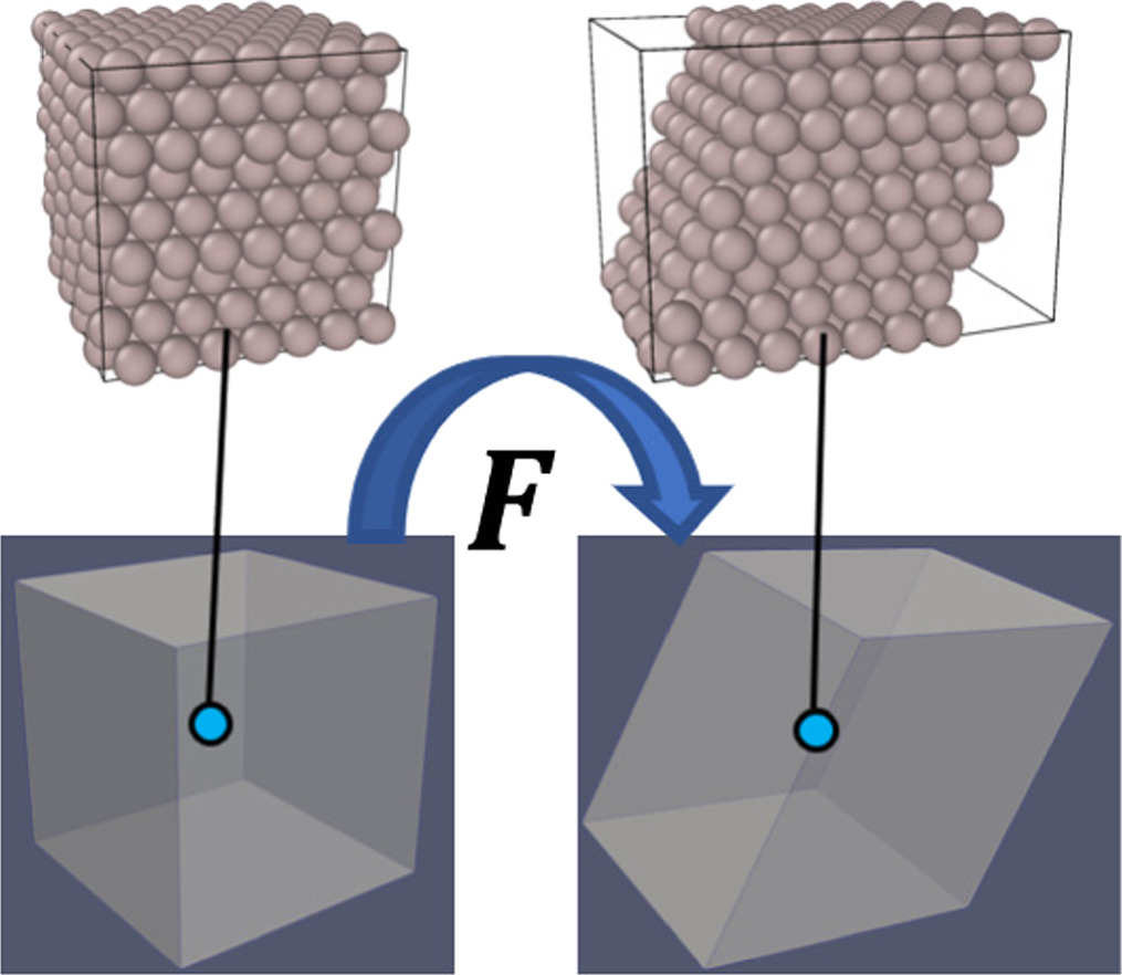
Figure 1. The schematic illustration of coupling the atomistic-scale simulation cells with the deformation of a continuum using CBR. The positions of the atoms follow the continuum-scale deformation gradient.
Download figure:
Standard image High-resolution image3.2. Coupling molecular dynamics model with finite element method using Cauchy-Born rule
The method of coupling the MD model with the FEM using the concept of CBR is explained in this section. Figure 2 represents the multiscale computational algorithm employed in this study. Firstly, we prepare a representative MD simulation cell whose shape is described by a second-order shape tensor H . Each computational cell used in MD is virtually related to a Gauss quadrature IP of a finite element model, as shown in figure 3. Each MD simulation representing the corresponding integration point of the finite element is independent of each other. Direct communication between the MD cells is not considered as each cell is made of a locally periodic nano-scale structure that has a large distance from other cells at a macroscale. The atom position vector r i (k) for an atom i in a representative unit cell at time increment k can be expressed as


where F IP(k) is the deformation gradient tensor of IP at time increment k in the finite element model and H IP(0) is the initial shape of the representative MD unit cell. The shape tensor H IP(k) prescribes the shape of the unit cell at step k. However, F IP(k) is, in general, not symmetric and has nine independent components. The rotation component of the deformation gradient tensor needs to be removed so as not to allow a rigid body rotation of MD unit cells. To this end, we introduce the QR decomposition to eliminate the rotation components. Using the QR decomposition by the Gram-Schmidt orthogonalization, the deformation gradient tensor F IP(k) is decomposed into the orthogonal rotation tensor Q IP(k) and the upper triangular stretch tensor R IP(k):

The upper triangular stretch tensor R IP(k) satisfies the periodic boundary conditions on the orthogonal basis of the unit cell. Therefore, instead of using the full F IP(k), we use R IP(k) to apply the deformation to the unit cell:

In an incremental form, equation (15) can be rewritten as

where the increment Δ R IP(k) is obtained using the values at the previous step k − 1 and the current step k as,

Therefore, new atomic coordinates are estimated based on the previous atom position vector  :
:

After equation (18) is prescribed, the coordinates of the atoms within the unit cell are determined by minimizing the total potential energy to approximate the equilibrium state. Next, the information about the atom coordinates and forces is used for the evaluation of the stress and the analysis of the crystal structure.
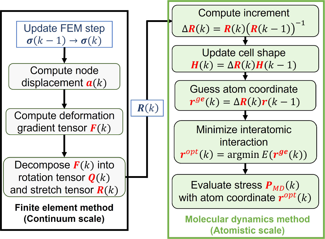
Figure 2. Multiscale computational algorithm. The finite element analysis part is first performed, and then the molecular dynamics part is computed with the deformation tensor from the finite element analysis. The FEM part in this schematic diagram assumes fixed displacements on some of the nodes.
Download figure:
Standard image High-resolution image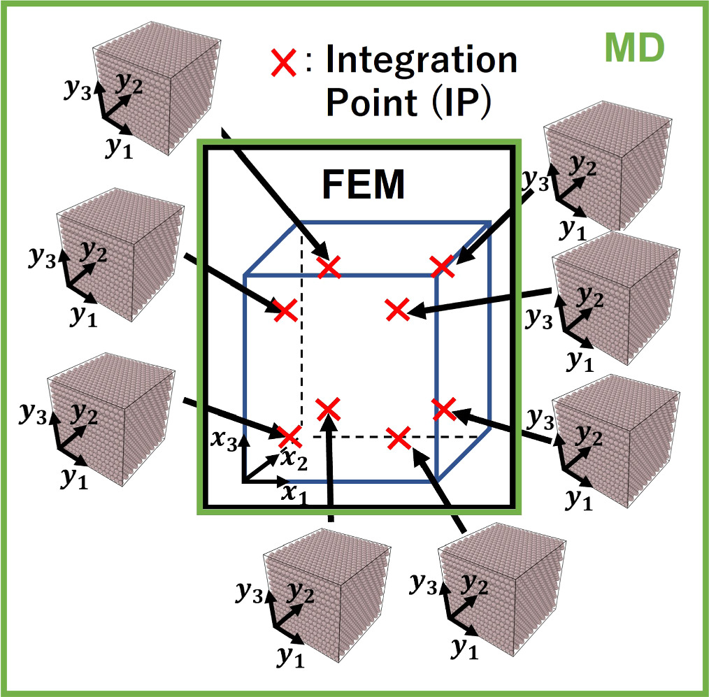
Figure 3. The schematic illustration of nanocrystalline atomistic models connected to the IPs of a continuum finite element. Each IP is used to pass the deformation history to the nanocrystalline model.
Download figure:
Standard image High-resolution image4. Modeling setup and numerical examples
This section describes the models and the loading conditions used in the multiscale simulations and presents the numerical examples illustrating the FE
4.1. Macroscale model
At the continuum macroscale, a cubic model with an edge length of 0.4 mm is considered. This macroscopic domain is discretized with a single isoparametric linear eight-node hexahedral element with eight IPs. The macroscopic element with the nodes and the IPs are depicted in figure 4(a).
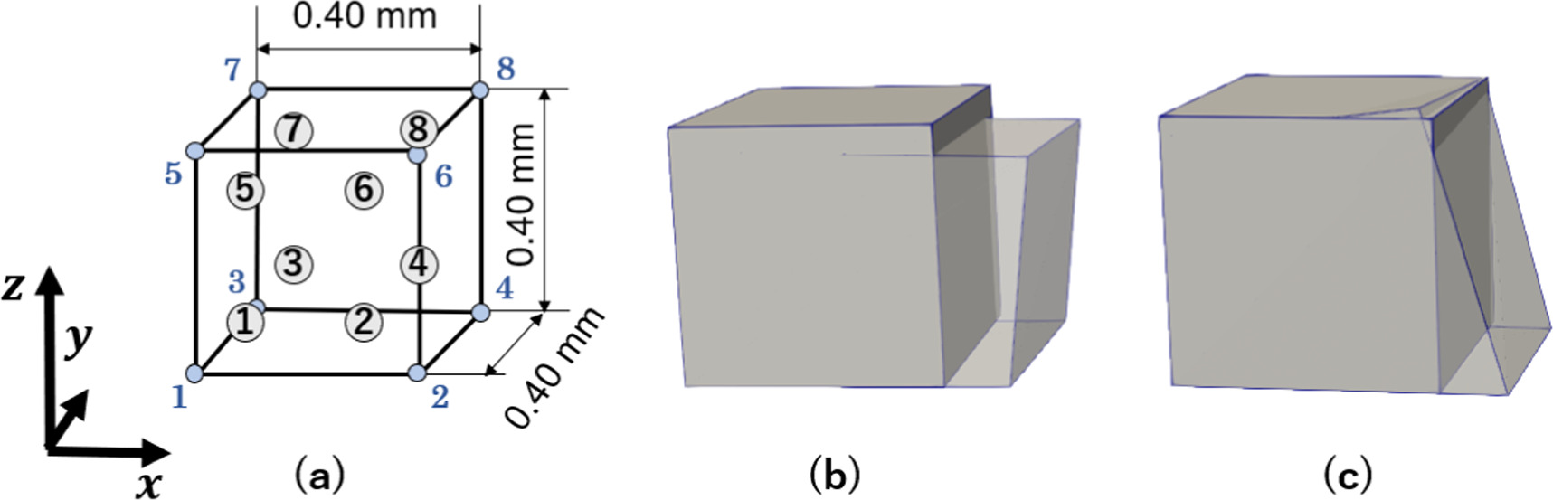
Figure 4. Macroscopic model: (a) the model dimensions and the numbering of the nodes (blue) and the IPs (encircled). (b), (c) the undeformed and deformed geometries are shown for loading case 1 and loading case 2. The boundary conditions are provided in table 1. The deformed states are scaled by a factor of 2 for better visualization.
Download figure:
Standard image High-resolution image4.2. Non-uniform tension loading cases
Two non-uniform tensile loading cases, which are described in the following parts, are applied to the macroscopic domain. In both loading cases, three faces on the left, the bottom, and the front were fixed with sliding allowed; that is, node 1 was fully fixed, node 2 was fixed in the y- and z-directions, node 5 in the x- and y-directions, node 3 in the x- and z-directions, node 7 in the x-direction, node 6 in the y-direction, and node 4 in the z-direction. In loading case 1 (figure 4(b)), we prescribe different values of displacements to nodes 2, 4, 6, and 8 on the right side of the element, shown in figure 4(b). Displacements in the x-direction of 0.05 mm, 0.06 mm, 0.07 mm, and 0.08 mm were given to nodes 2, 4, 6, and 8, respectively. In loading case 2 (figure 4(c)), only nodes 2 and 4 were given displacements of 0.05 mm in the x-direction. For both loading cases, the total displacements were applied in 30 steps. After the simulation of one step in FEM was completed, the deformation state of all nanocrystalline models corresponding to different IPs was updated accordingly. The prescribed boundary conditions on the nodes are summarized in table 1.
Table 1. List of displacement boundary conditions applied to the nodes of the macroscopic model; Here, ax , ay , az denote the prescribed displacements as constraints in the x-, y-, and z-directions respectively, and 'free' means the node is free to move in the specified direction. The unit of length is in mm.
| Node | 1 | 2 | 3 | 4 | 5 | 6 | 7 | 8 | |
|---|---|---|---|---|---|---|---|---|---|
| Case 1 (figure 4(b)) | ax | 0 | 0.05 | 0 | 0.06 | 0 | 0.07 | 0 | 0.08 |
| ay | 0 | 0 | free | free | 0 | 0 | free | free | |
| az | 0 | 0 | 0 | 0 | free | free | free | free | |
| Case 2 (figure 4(c)) | ax | 0 | 0.05 | 0 | 0.05 | 0 | free | 0 | free |
| ay | 0 | 0 | free | free | 0 | 0 | free | free | |
| az | 0 | 0 | 0 | 0 | free | free | free | free |
4.3. Nanocrystalline models
At the MD scale, a nanocrystalline aluminum model is considered, which consists of four hexagonal grains with almost identical grain sizes; see figure 5. The MD model was generated using Atomsk [51]. The unit cell has a cubic shape, with each side being approximately 30 nm; see appendix A on how the size of the unit cell was chosen. We consider that the columnar-structured nanocrystalline model is sufficient to demonstrate the FEM-MD method, at this moment, not aiming at an in-depth study of the detailed deformation mechanisms of nanocrystalline aluminum. Nevertheless, grain size has been selected such that the typical behavior of nanocrystalline aluminum is well represented; see appendix A. The crystal orientation of the grain labeled (a) is defined as x [−1 1 0] y [−1−1 2] z [1 1 1]. The grains labeled (b), (c), and (d) have the same crystal orientation in the z-direction but different x- and y-directions obtained by the counterclockwise rotation around the z-axis by 30°, 60°, and 90°, respectively, from the crystal orientation of grain (a); see table 2. This configuration is denoted as nanocrystalline model A. The distinct crystal orientations generate the grain boundaries appearing as gray-colored regions in figure 5. Another nanocrystalline model B has a different crystal orientation pattern. In model B, the crystal orientation of each grain was rotated 45 degrees around the z-axis from the original orientation in nanocrystalline model A; see table 2.
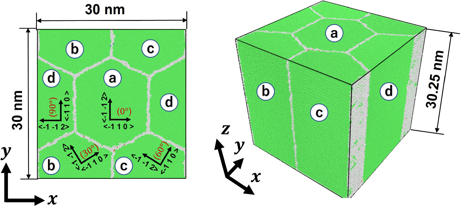
Figure 5. Nanocrystalline model used in this study. The grains labeled (a), (b), (c), and (d) have different orientations in the (x,y)-plane given by the axis shown on each grain. Gray areas expose the grain boundaries.
Download figure:
Standard image High-resolution imageTable 2. Grain orientations in the two considered nanocrystalline models. The degrees are the angles of rotation around the z-axis from the original crystal orientation with respect to the x, y, and z-axes.
| Nanocrystalline model A | Nanocrystalline model B | |||||
|---|---|---|---|---|---|---|
| Grain | x-axis | y-axis | z-axis | x-axis | y-axis | z-axis |
| [−1 1 0] | [−1−1 2] | [1 1 1] | [−1 1 0] | [−1−1 2] | [1 1 1] | |
| (a) | 0° | 0° | 0° | 45° | 45° | 0° |
| (b) | 30° | 30° | 0° | 75° | 75° | 0° |
| (c) | 60° | 60° | 0° | 105° | 105° | 0° |
| (d) | 90° | 90° | 0° | 135° | 135° | 0° |
4.4. MD simulation settings
The MD simulations were performed in LAMMPS [43]. Periodic boundary conditions were applied to all MD cell boundaries. Mishin's EAM was chosen as the interatomic potential [48]. After the generation of the nanocrystalline models, initial relaxation of the unit cells was performed. It took 20 000 steps (20ps) for each computation in the NPT ensemble, in which the pressure 0 Pa and the temperature 300 K are kept constant. The unit cell of the nanocrystalline model was assumed to be embedded in each IP. The deformation information was passed to the computational cell of the MD method through the connection between each IP and the MD model. For simplicity, the position vector defined in equation (18) was applied only in the x-direction to the MD unit cells. The y- and z-directions were pressure-controlled. The MD computations to deform each computational cell were conducted at a constant temperature of 300 K and a constant pressure of 0 Pa in the y- and z-directions. Each computation of a deformation phase took 500 steps, which is 0.5 ps in the time unit. After the unit cell had finished the prescribed deformation process, a relaxation phase was inserted to make the systems close to equilibrium states. The relaxation of the system was performed for 35,000 steps (35 ps) at constant pressure with the temperature set at 300 K; see appendix B for the study on the length of relaxation time. After the computation of the relaxation had finished, we conducted the Common Neighbor Analysis (CNA) to observe the nucleation and the growth of defects such as deformation twins and stacking fault [52]. These processes were repeated until all the computation steps prescribed on the FEM side were done.
4.5. Loading case 1 with nanocrystalline model A
The macroscopic deformation of loading case 1 is shown in figure 4(b). Four distinct deformation gradient values at IPs 1 and 2, 3 and 4, 5 and 6, and 7 and 8 were obtained for this loading. The effective stress-strain responses resulting from the MD simulations are shown in figure 6. It is argued that strain softening occurred at all the IPs after reaching the yield strain of approximately 0.025. The trend of the yield strains agrees well with that obtained in the experimental tensile test of nanocrystalline aluminum [53], both of which have a yield strain between 0.02 and 0.025. The yield stress differs between the MD simulation and the experiment due to the high strain rate in the MD simulation.
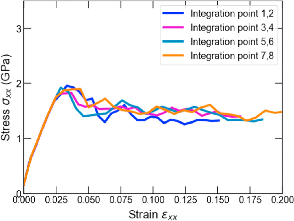
Figure 6. The effective stress-strain curves obtained from the MD models for the xx-components at corresponding different macroscale IPs in non-uniform tensile loading case 1.
Download figure:
Standard image High-resolution imageWe also assessed the ratio of hexagonal close-packed (hcp) atoms with respect to the total number of atoms in the model at every FEM step after the relaxation phase in MD computations to investigate the nucleation of crystal defects. The number of hcp atoms is considered in the discussion primarily to demonstrate that the stress-strain response correlates with the onset and evolution of stacking faults or twins. As shown in figure 7, an increasing trend in the number of hcp atoms is observed after passing the yield strain value. The results also show that the hcp ratio at IPs 1 and 2 was, on average, higher than at the other IPs. The highest hcp ratio at IPs1 and 2 was 0.0190, whereas the lowest value was 0.0118 at IPs7 and 8. Figure 8 shows the crystal structure in cross-section at z = 20 mm at selected FEM steps after relaxation. Multiple deformation twins crossing the central grain in the diagonal direction were observed in the nanocrystalline MD models at IPs 1 and 2, as shown in figures 8(a) and (b). At IPs 3 and 4, on the other hand, only a few crystal defects in the nanocrystalline MD models occurred, which were also confirmed by a low hcp ratio in the plastic deformation stage. Here, we observed that the stacking faults that existed at the applied strain εxx = 0.053 in figure 8(c) vanished at εxx = 0.053 in figure 8(d). While some stacking faults disappeared, other defects were nucleated at the same time. This phenomenon also occurred for the stacking faults and deformation twins at other locations at IPs 7 and 8, as seen in figure 8(h).d Further investigation into the behavior of defects was conducted by studying the crystal structure changes during the relaxation, shown in figures 9 and 10. These snapshots exhibit the appearance, annihilation, and migration of crystal defects in the course of the relaxation. At the beginning of the relaxation figure 9(a), no crystal defects are present, whereas the defects represented by red lines are confirmed in figure 9(d). Similar observations are made in figures 9(e)–(h). The snapshots in figures 9(e)–(h) exhibit the formation of deformation twins at the early stage of the relaxation, and the size of the twins grows in the course of the relaxation. The crystal structure change during the next relaxation phase following the next loading step is shown in figure 10. The annihilation of defects is observed in figures 10(b)–(d). Furthermore, detwinning is observed in figures 10(f)–(h). The onset of various crystal structure changes, those shown in the snapshots in figures 9 and 10, typically originates from the emission of defects from the grain boundaries as indicated in figure 11, see also the supplementary video. Compared to the initial configuration shown in figure 5, the grain boundaries after loading are not neatly aligned and are somewhat jagged. Previous studies have already revealed that these disordered grain boundaries, called nonequilibrium grain boundaries (NEGBs), induce atomic shuffling and rearrangement in the MD simulation [54, 55]. Similar observations have also been confirmed in the experimental investigation into nanocrystalline materials as well [56, 57]. The present work considers more complicated grain structures and deformation history than those in the previous studies and thus suggests that the interaction between NEGBs could result in the onset and annihilation of deformation twins during relaxation.
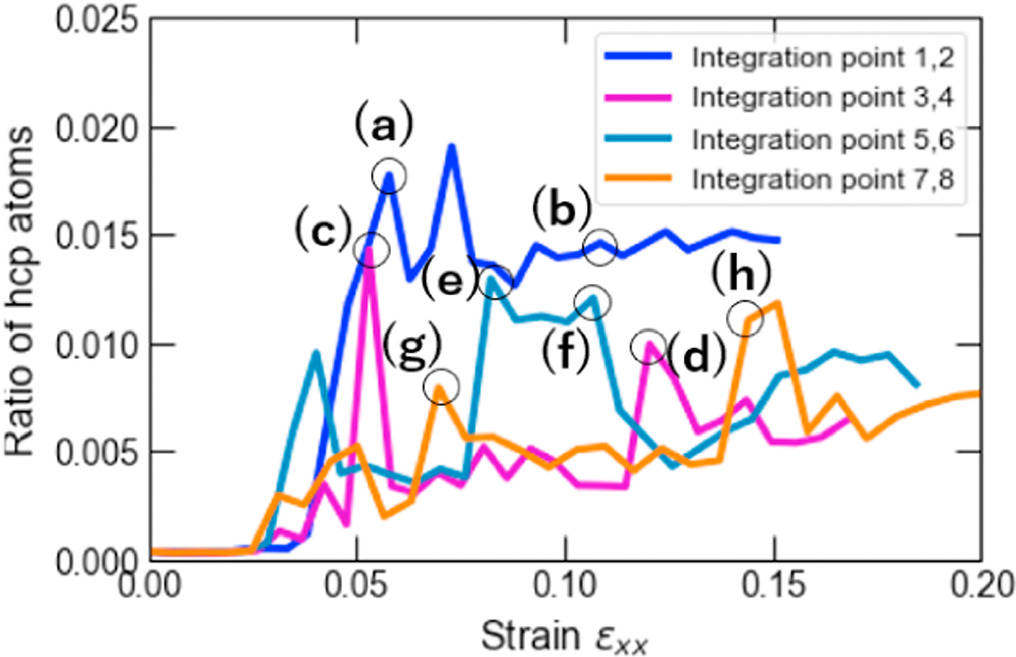
Figure 7. Ratio of hcp-structure atoms to the total number of atoms as a function of the applied xx-strain component in non-uniform tensile loading case 1 corresponding to different macroscale IPs.
Download figure:
Standard image High-resolution image
Figure 8. xy-plane cross sections of crystal structures at the highest hcp-ratio points corresponding to different macroscale IPs at z = 20 nm in non-uniform tensile loading case 1. Hcp atoms are colored red.
Download figure:
Standard image High-resolution image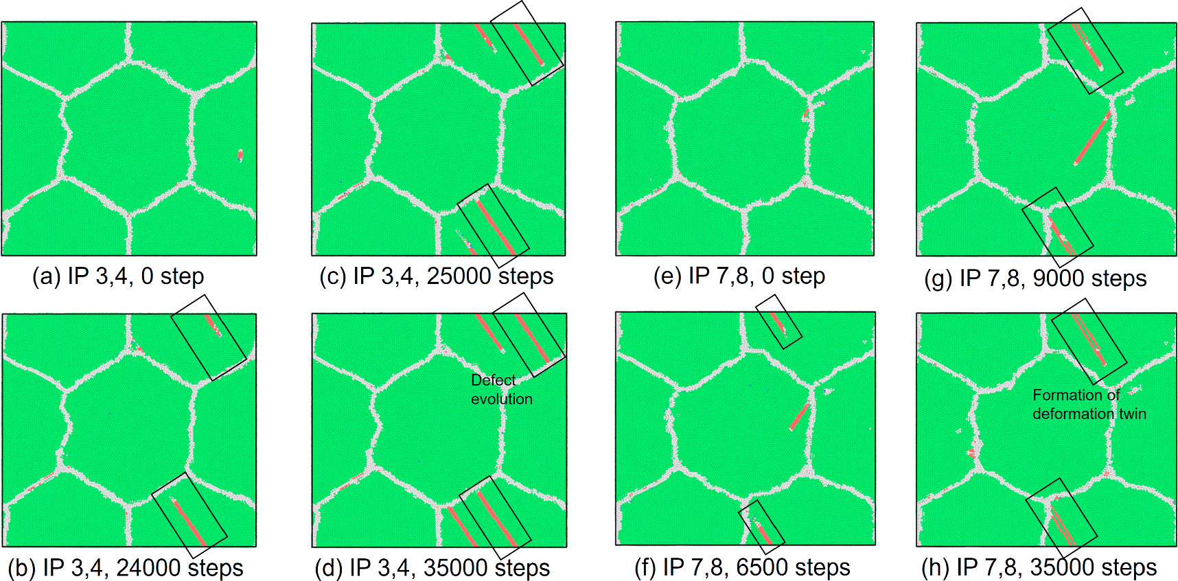
Figure 9. Cross sections of crystal structures at the maximum hcp-ratio points during relaxation at IPs 3, 4, 7, and 8 on xy-plane at z = 20 nm in non-uniform tensile loading case 1. Figures (a)–(d) are at εxx = 0.053 as in figure 8(c). Figures (e)–(h) are at εxx = 0.070 as in figure 8(g). Hcp atoms are colored red.
Download figure:
Standard image High-resolution image
Figure 10. Cross sections of crystal structures at the maximum hcp-ratio points during relaxation at IPs 3, 4, 7, and 8 on xy-plane at z = 20 nm in non-uniform tensile loading case 1. Figures (a)-(d) are at εxx = 0.060, which is the next FEM loading step of the state shown in figure 8(c). Figures (e)-(h) are at εxx = 0.076, which is the next FEM step after the state shown figure 8(g).
Download figure:
Standard image High-resolution image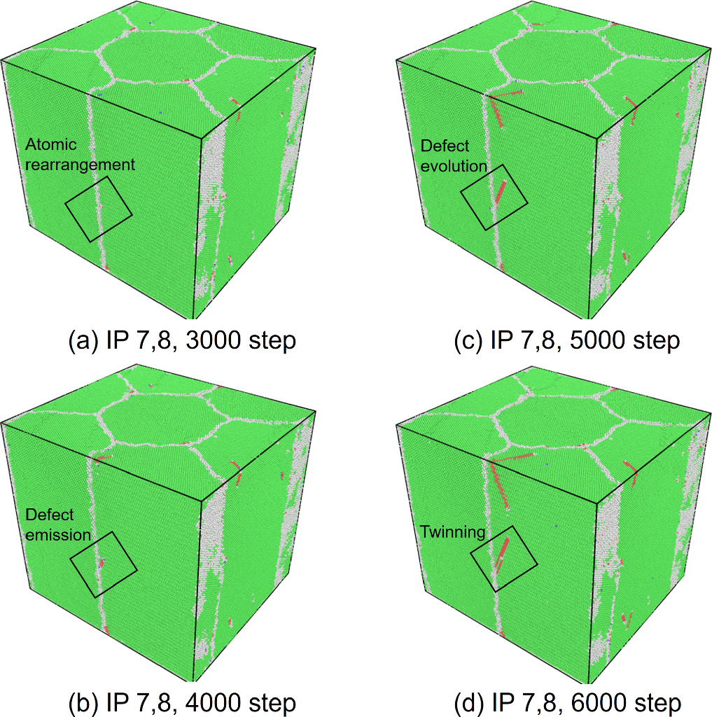
Figure 11. Crystal structure change in the unit cell at the maximum hcp-ratio points during relaxation at IPs 7 and 8 in non-uniform tensile loading case 1 at εxx = 0.053 as in figure 8(c).
Download figure:
Standard image High-resolution image4.6. Loading case 2 with nanocrystalline model A
From the deformation shown in figure 4(c), four distinct deformation patterns were obtained at IPs 1 and 2, 3 and 4, 5 and 6, and 7 and 8, as well as in case 1. The effective MD stress-strain curves for the xx component obtained at corresponding IPs are shown in figure 12. While strain softening was confirmed at IPs 1-4, the stress response remained elastic at IPs 5-8 because of the small deformation prescribed on the unit cells. The result of figure 13 indicates that the number of hcp atoms increased at IPs 1-4, which is attributed to the onset or growth of defects after reaching the yield point. The ratios of hcp atoms for IPs 5-8 are not plotted since they remained almost zero during the whole simulation. The snapshots of crystal structure in figure 14 show that IPs 1 and 2 contained deformation twinning under deformation. On the other hand, no deformation twin was found at IPs 3 and 4, although stacking faults and some other defects were observed in figure 14(c). It is also noteworthy that in both configurations, the grain boundaries are no more as straight as they are in the initial configuration. As discussed in loading case 1, it is suggested that NEGBs also came into play in the formulation and annihilation of stacking faults and deformation twins under this loading pattern.
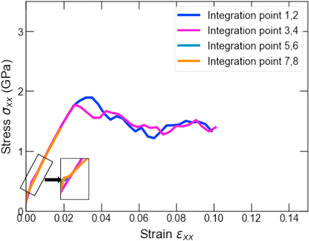
Figure 12. The effective stress-strain curves obtained from the MD models for the xx-components at corresponding different macroscale IPs in non-uniform tensile loading case 2.
Download figure:
Standard image High-resolution image
Figure 13. Ratio of hcp-structure atoms to the total number of atoms as a function of the applied xx-strain component in non-uniform tensile loading case 2 corresponding to different macroscale IPs.
Download figure:
Standard image High-resolution image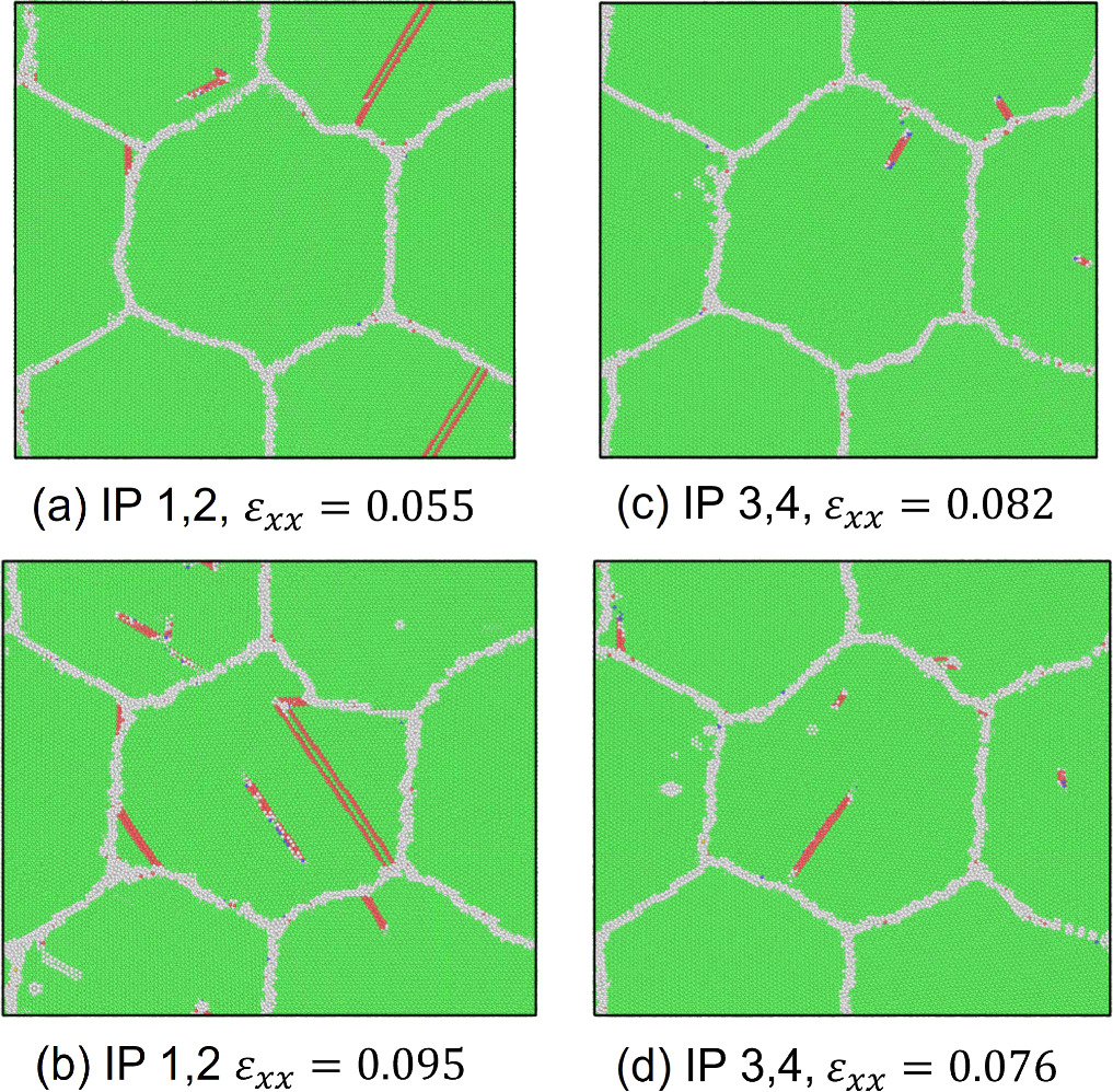
Figure 14. xy-plane cross sections of crystal structures at the highest hcp-ratio points corresponding to different macroscale IPs at z = 20 nm in non-uniform tensile loading case 2. Hcp atoms are colored red.
Download figure:
Standard image High-resolution image4.7. Loading case 1 with nanocrystalline model B
The deformation experienced at each IP is identical to loading case 1. The effective stress-strain curves shown in figure 15 and the result of CNA provided in figure 16 showed the different responses from those obtained from the simulation for nanocrystalline model A. Figure 15 confirmed that the maximum stress was reached at a strain of approximately 0.04, similar to the other two cases. Notably, the increase in the ratio of hpc atoms in figure 16 was smaller than in the case of the nanocrystalline model A as in figure 7. In this case, the hcp ratio at a strain of 0.05 is below 0.005. On the other hand, looking at figures 7 and 13, one can see that in the other two cases, the hcp ratio at a strain of 0.05 is higher than even 0.01. Since the increase in the number of hcp atoms is associated with the evolution of crystal defects, this observation indicates orientation-dependent defect activities, which have been observed in experiments and simulations on conventional metals and nanocrystalline metals. We confirmed that more crystal defects were generated in nanocrystalline model A in figure 8 compared to figure 17. However, onsets of stacking faults were still observed in nanocrystalline model B. No deformation twin was found in figures 17(a)–(d), which can also be explained by the orientation dependency. Furthermore, NEGBs are also seen in figure 17 in comparison with the initial configuration in figure 5, which infers the interplay of NEGBs in the case of nanocrystalline model B as well.
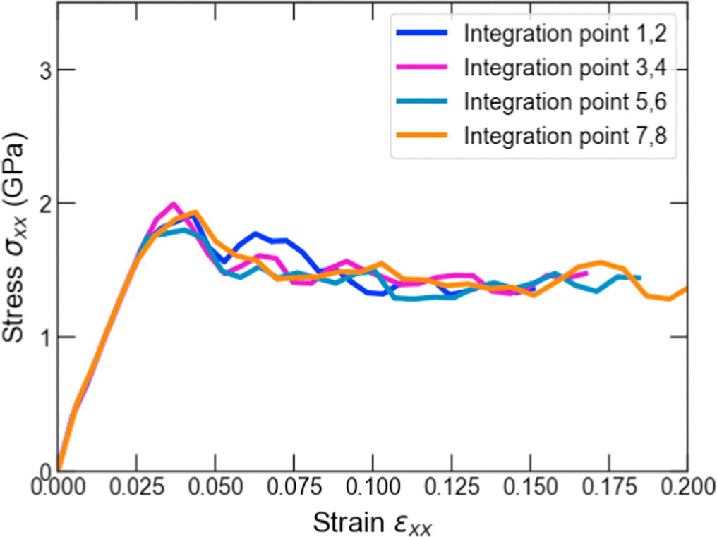
Figure 15. The effective stress-strain curves obtained from the MD models with a different crystal orientation (nanocrystalline model B) pattern for the xx-components at corresponding different macroscale IPs in non-uniform tensile loading case 1.
Download figure:
Standard image High-resolution image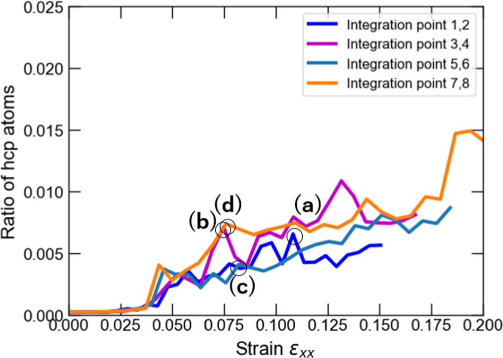
Figure 16. Ratio of hcp-structure atoms to the total number of atoms as a function of the applied xx-strain component in non-uniform tensile loading case 1 with nanocrystalline model B corresponding to different macroscale IPs.
Download figure:
Standard image High-resolution image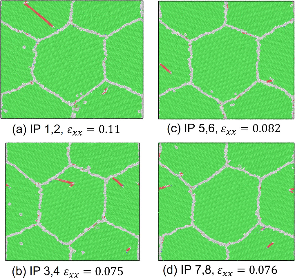
Figure 17. xy-plane cross sections of crystal structures at the highest hcp-ratio points corresponding to different macroscale IPs at z = 20 nm in non-uniform tensile loading case 1 with nanocrystalline model B. Hcp atoms are colored red.
Download figure:
Standard image High-resolution imageTo summarize, the developed FEM-MD multiscale method allows observation of the evolution of various dislocation patterns, including stacking faults and deformation twins, in the atomistic nanocrystalline model as a response to the deformation history originating from the macro-scale FEM. Regarding validation, the yield strain and crystal structure changes show good qualitative agreement with experimental observations. The variation of the results among different IPs is the most pronounced when some IPs do not show any defect evolution while others do. Furthermore, the extent of generation of stacking faults and deformation twins varies between IPs, exhibiting different dislocation nucleation patterns depending on the local macroscale deformation scenarios. Another remark is that different realistic microstructural evolution patterns are seen depending on the combination of different deformation scenarios and crystal orientations, which provides guidelines for the optimum material design of nanocrystalline materials. On the other hand, one of the limitations lies in that certain extreme loading conditions, such as twisting and bending, cannot be modeled in the MD simulation using the present implementation. Another limitation is the computational cost if a large model is employed. One of the solutions to this problem is to utilize k-means clustering on integration points with similar deformation patterns, leading to a reduction in computational cost. The employment of k-means clustering has already been demonstrated in some studies on the homogenization method [58–60]. Nevertheless, the present method can evaluate the dislocation dynamics of nanocrystalline models that contain multiple grains based on realistic macroscale deformation history.
5. Conclusion
This study proposed a continuum-atomistic bridging FEM-MD method for an efficient multiscale simulation of nanocrystalline metals. The FEM and MD method were employed for the continuum and atomistic-scale simulations, respectively. Nanocrystalline aluminum was chosen to validate the proposed method. The simulations of three test cases, which include two loading cases and two nanocrystalline models, were performed. The results from the two deformation cases exhibited distinct but similar stress responses. Looking at the crystal structure changes for every FEM step, we confirmed the onset and annihilation of defects, including deformation twins. Those atomistic-scale structure changes occurred during relaxation, during which NEGBs played a critical role in the onset and annihilation of defects. Furthermore, the results from the two crystal orientation patterns, namely nanocrystalline models A and B, confirmed the orientation dependency of the formation of plane defects since the increases in the number of hcp atoms were different between the simulation results of the two nanocrystalline models. To conclude, this method has an ideal property for investigating dislocation behaviors of nanocrystalline materials, namely multi-grained nanostructure. The bridging of a large scale gap from a nano-scale to a continuum scale is possible with the present method compared to other embedding methods. Along with the good qualitative agreement with experimental observations, the results discussed in the numerical examples suggest that the present FEM-MD method is capable of simulating multiple nanocrystalline models that deform corresponding to realistic deformation at a continuum scale simultaneously.
Data availability statement
The data cannot be made publicly available upon publication because no suitable repository exists for hosting data in this field of study. The data that support the findings of this study are available upon reasonable request from the authors.
Appendix A.: Width of nanocrystalline models
The size of the unit cell should be sufficiently large so that the simulation results are not affected by artifacts of periodic boundaries. To examine the validity of the cell size, nanocrystalline models with different cell sizes were prepared. Simulations for six different thicknesses in the z-direction, 1 nm, 2 nm, 3 nm, 5 nm, 15 nm, and 30 nm, were performed to compare the stresses at each strain obtained from MD simulations. The boundary conditions, control method, potential, and other simulation conditions were set identically for all cases. For initial relaxation, the pressure in all directions was set to 0 Pa, and the computation took 20,000 steps (20 ps) to finish. Then each unit cell was pulled in the x-direction. During the deformation of the computation cell, the strain rate in the tensile direction was set to 10/ ns. The computation was carried out for 20,000 steps (20 ps) so that the final strain was 0.2. Strain control was employed with the canonical ensemble in the x-direction, and in the y- and z-directions, pressure control with the isobaric isothermal ensemble was used. For the entire simulation, we set the boundary surfaces as periodic boundaries in all three directions. Mishin's EAM was employed for the potential function. The temperature was adjusted at 300 K, and the length of a timestep for the computation was 1 ps.
The xx-component stress-strain curves obtained from the computations for each z-direction thickness of the nanocrystalline model are shown in figure B1. The case of the model with a thickness of 1.5 nm in the z-direction showed a large deviation in the stress values compared to that with a thickness of 30 nm. This is due to the fact that the cutoff radius of the potential used is 0.6287nm, and 1.5 nm is quite close to twice that value of about 1.25 nm. It was also confirmed that the stress values for the 2 nm, 3 nm, and 5 nm specimens differed from those for the 30 nm specimen. On the other hand, the stress-strain curves with z-direction thicknesses of 15 nm and 30 nm were almost identical, suggesting that the model size of 15 nm or larger than 15 nm is not significantly affected by the periodic boundary artifact. The average absolute difference between the two curves is 0.041 GPa, which is small enough given that the stress values are within a range of 1.5-3.0 GPa. Since the model used in this study has a cubic shape with one side of 30 nm, we assert that this model size is large enough not to be significantly influenced by periodic boundaries.

Figure B1. MD effective stress-strain curve for the xx component obtained from the computations of each thickness in the z direction. The values on the legend represent the thickness of the nanocrystalline model along the z-axis.
Download figure:
Standard image High-resolution imageAppendix B.: Relaxation time for post-deformed unit cells
The tensile loading is applied in a non-equilibrium condition in the MD method, meaning that the atomic configuration obtained at each step does not represent the static state of the system. The finite element method, on the other hand, is a static analysis in which the position of nodes constituting the model is determined such that an equilibrium state holds based on the principle of virtual work. Therefore, to make both analyses consistent in the perspective of equilibrium, it is essential to introduce a relaxation process to the MD simulations after deformation so that atomic states after deformation are as close to the equilibrium state as possible. To determine the number of steps required to equilibrate the system, relaxation with a constant temperature and a constant volume was performed on a unit cell with different strains. The initial relaxation was performed for 20,000 steps (20 ps), setting the pressure 0 Pa in all directions as used in the model size validation. During the deformation phase, the strain rate in the tensile direction was set to 10/ ns, and the computation took 6500 steps (0.65 ps) or 8500 steps (0.85 ps) so that the final strain was 0.065 or 0.085. The x-direction was strain-controlled, and the y- and z-directions were pressure-controlled. The same boundary conditions and interatomic potential were used for the computations of the deformation. The deformation step in each MD simulation was followed by the relaxation step, which was set to 50,000 steps (50 ns) to finish. We set the temperature at 300 K. Periodic boundaries and Mishin's EAM was adopted for the system as the boundary condition and the interatomic potential, respectively.
According to the kinetic energy change during the relaxation shown in figure B2, the system reached almost equilibrium for both cases. The final value of the kinetic energy was approximately 63 000eV. The change in stress xx-, yy-, and zz-components during the relaxation shown in figure B3 also indicates that the values of each stress moved toward convergence. The convergence values differed at strains of 0.065 and 0.085, which is attributed to the difference in atomic positions and allowed movement of each atom due to the different cell geometry. The result in figure B3 also confirmed that all the stress components converged after the relaxation of around 35,000 timesteps. From a quantitative point of view, the standard deviations of the stress between 35 000 and 50 000 timesteps in the xx-, yy-, and zz-components are 0.0034 GPa, 0.0058 GPa, and 0.0096 GPa, respectively. These values are small enough compared to the converged stress values of 1-2 GPa. This result shows that we can equilibrate the MD unit cell adequately by setting the length of time for the relaxation at 35,000 timesteps, equivalent to 35 fs, with a timestep width of 1 fs in our multiscale simulations.
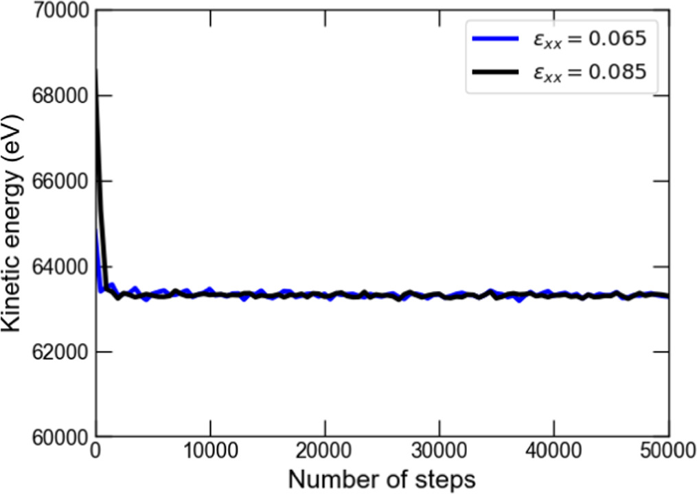
Figure B2. Fluctuation of kinetic energy during the computation of relaxation.
Download figure:
Standard image High-resolution image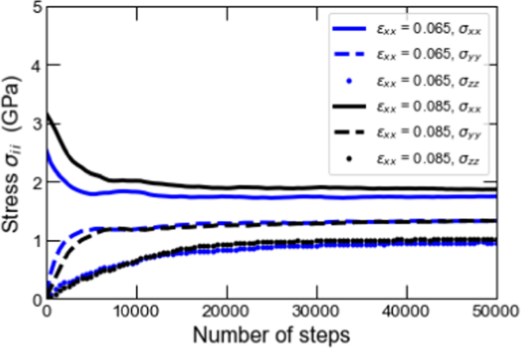
Figure B3. Fluctuation of the stresses in the xx, yy, and zz components with a given strain 0.065 and 0.085 during the computation of relaxation.
Download figure:
Standard image High-resolution image
Supplementary data (6.1 MB MP4)