

Abstract
The crystal structure, formation energy, electronic structure, electrical properties and optical properties of anatase TiO2 with various Nb concentrations were studied by first-principles calculations based on density functional theory (DFT) and the Hubbard U correction. Firstly, the crystal structures of TiO2 with various Nb concentrations were optimized successfully. The higher concentrations of Nb facilitate the synthesis of Nb-doped TiO2 systems in an O-rich environment. Furthermore, the band structures and density of states prove that the electronic structure of Nb-doped TiO2 is mainly transformed by the hybridization of Ti 3d, Nb 4d and O 2p states. Next, broadening of the valence band and occupied states at the bottom of the conduction band enhance the conductivity of Nb-doped TiO2, and the conductivity reaches the maximum value at the high Nb-doping concentration of 6.25 at.%. Last but not least, the calculated optical properties show that the absorption edge of Nb-doped TiO2 produces an blue shift. TiO2 with Nb-doping concentration below 14.58 at.% exhibits the high transmittance in the visible region.
Export citation and abstract BibTeX RIS
1. Introduction
Transparent conducting oxide (TCO) plays significant roles in various fields including sensors, heat mirrors, displays, active energy generation and optoelectronic devices, etc [1–4]. In different TCO materials, Sn-doped In2O3 (ITO) is widely applied thanks to its excellent electrical and optical properties [5]. However, Because indium is scarce and expensive, which promotes researchers to search for alternatives to prepare indium-free TCO materials. In 2005, Furubayashi et al [6] prepared Nb-doped anatase TiO2 (TNO) films on a SrTiO3 substrate by pulsed laser deposition (PLD) method, the excellent resistivity (2 ∼ 3 × 10⁻⁴ Ω cm) and visible transmittance (>90%) of the innovated film are comparable to that of typical TCOs. Subsequently, other researchers studied the properties of TNO films created by different preparation methods [7–12]. TNO is expected to become the next generation of innovated TCO material.
For theoretical calculation, existing works of literature have revealed the deep reason of TNO conductivity based on density functional theory (DFT) [13, 14]. Orita [15] investigated the metallization mechanism of TNO via GGA + U method [16, 17], considering the strongly correlated interactions between the Ti d-orbital electrons, and found that metallization was majorly attributed to the direct doping of an excess electron of Nb to the hybridized bands consisting mainly of Ti and Nb d-orbitals. Similarly, the electronic properties of pentavalention (Nb5+, Ta5+, and I5+) doped anatase and rutile TiO2 were studied by same method [18]. However, overly small Ud value for Ti atom will cause the band gap of TiO2 failing to reach the experimental value, and overly large Ud value will produce some unphysical phenomena. The problem can be solved by introducing the Hubbard U parameter on the p-orbital electrons of oxygen (Up).
In this study, first-principles calculations employing the DFT + Ud+Up approach are performed to investigate the individual effects of different Nb concentrations on the crystal structure, formation energy, electronic structure, electrical properties and optical properties of Nb-doped anatase TiO2. The work is rather important and meaningful for the preparation and application of TNO in multiple aspects.
2. Calculation models and methods
In order to form an appropriate doping concentration of Nb, a 2 × 2 × 1 anatase TiO2 supercell was constructed with 16 Ti and 32 O atoms, as shown in figure 1(a). Considering that the formation energy of the substitutional model was lower than that of the interstitial doping model, the doping concentrations of 2.08%, 4.17%, 6.25%, 10.42% and 14.58% were obtained respectively by replacing Ti atoms with 1, 2, 3, 5 and 7 Nb atoms in the 48-atom supercell.
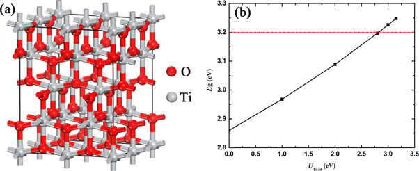
Figure 1. (a) 2 × 2 × 1 anatase TiO2 supercell model. (b) Band gap (Eg) for anatase TiO2 as a function of UTi-3d parameter with UO-2p fixed at 5.25 eV.
Download figure:
Standard image High-resolution imageThe density functional calculation software package CASTEP [19] was employed to calculate the structural, electronic and optical properties of Nb-doped anatase TiO2. Vanderbilt-form ultrasoft pseudopotentials [20] with valence electron configurations of 3s23p63d24s2 for Ti, 2s22p4 for O, and 4s24p64d45s1 for Nb were applied to describe the interactions between the ionic core and valence electrons. The exchange and correlation potential are modeled by the generalized gradient approximation (GGA) Perdew-Becke-Erzenhof (PBE) function [21]. The plane- wave basis sets are generated using a cutoff energy of 680 eV. The Monkhorst-Pack scheme [22] K-points grid sampling was set as 4 × 4 × 3 in the first Brillouin zone. The convergence threshold for self-consistent iterations was set as 1 × 10⁻⁶ eV. In geometric optimization, the energy change, maximum force, maximum stress, and maximum displacement tolerances were set as 1 × 10⁻⁵ eV/atom, 0.03 eV/Å, 0.05 GPa, and 0.001 Å, respectively.
DFT + Ud+Up method was adopted to describe the Coulomb interactions of Ti 3d and O 2p orbital electrons. Auger spectroscopy studies of different oxides demonstrated that the on-site Coulomb interaction energy for a hole in an O 2p orbital was 5 ∼ 7 eV [23, 24]. Ma et al also obtained similar results by studying the influence of U value for O 2p orbital electrons on the band gap of Ag3PO4 [25]. Therefore, UO-2p value of 5.25 eV was used in this work [26]. Figure 1(b) showed band gap (Eg) for anatase TiO2 as a function of UTi-3d parameter with UO-2p fixed at 5.25 eV. It could be observed that the band gap of anatase TiO2 increased with the increase of UTi-3d value. When UTi-3d = 2.8 eV, the band gap value of anatase TiO2 was 3.197 eV, which was highly consistent with the experimental value. In addition, the U value of Nb 4d orbital electrons was set as 4 eV [27].
3. Results and discussion
3.1. Structural optimization
The optimized lattice parameters, average bond lengths, and differences in volume at various Nb concentrations are listed in table 1. The lattice parameters of pure anatase TiO2 are calculated as a = b = 3.799 Å, c = 9.708 Å, close to the earlier theoretical works and experimental values [28–31], which indicates that the applied calculation methods are rational and the obtained results are reliable. In the crystal structure shown in figure 1(a), each Ti atom bonds to the nearest four oxygen horizontally and to the nearest two vertically. Average bond lengths in horizontal and vertical direction are represented as Ti–O1st and Ti–O2nd, respectively. With the increase of Nb-doping concentration, the volume increases gradually. This may be attributed to the difference in ion radii between Nb5+ (0.62 Å) and Ti4+ (0.56 Å) [32]. The bond length in the crystal varies accordingly after Nb atom replace Ti atom in an alternative way. In the crystal structure with the same Nb-doping concentration, the lengths of Nb–O1st and Nb–O2nd are longer than those of Ti–O1st and Ti–O2nd, respectively. As the number of substituted Ti atoms increases, the lengths of Ti–O1st, Ti–O2nd, and Nb–O1st become longer, eventually causing the overall volume to expand.
Table 1. Optimized lattice parameters, average bond lengths, and volume difference (ΔV) of TiO2 doped with various concentrations of Nb.
| Lattice parameters (Å) | Bond lengths (Å) | |||||||
|---|---|---|---|---|---|---|---|---|
| Nb (at.%) | a | b | c | Ti-O1st | Ti-O2nd | Nb-O1st | Nb-O2nd | ΔV (%) |
| 0 | 3.799 | 3.799 | 9.708 | 1.946 | 2.004 | — | — | — |
| 2.08 | 3.816 | 3.816 | 9.701 | 1.954 | 2.006 | 1.964 | 2.024 | 0.82 |
| 4.17 | 3.831 | 3.831 | 9.713 | 1.959 | 2.011 | 1.968 | 2.032 | 1.74 |
| 6.25 | 3.846 | 3.846 | 9.718 | 1.965 | 2.015 | 1.975 | 2.030 | 2.59 |
| 10.42 | 3.878 | 3.874 | 9.742 | 1.979 | 2.020 | 1.989 | 2.032 | 4.46 |
| 14.58 | 3.906 | 3.907 | 9.787 | 1.990 | 2.046 | 2.007 | 2.072 | 6.60 |
In order to further observe the changes of internal atomic position due to Nb-doping, the atomic positions and the bonds on the (010) plane are presented in figure 2. The corresponding bond lengths of pure TiO2 in figure 2(a) are set as a contrast. After Nb atom replace Ti atom, the Nb–O bond lengths along the [100] direction and most of the Nb–O bond lengths along the [001] direction are longer than those of pure TiO2. When the Nb-doping concentration is 14.58%, the bond lengths in these two directions appear the maximum value (2.039 Å and 2.253 Å), and the local lattice deteriorates the most seriously, which is consistent with the volume difference in table 1.
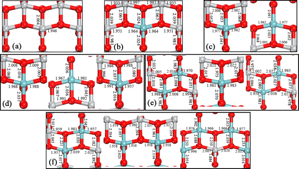
Figure 2. Optimized (0 1 0) plane atomic structures of TiO2 doped with Nb (a) 0 at.%, (b) 2.08 at.%, (c) 4.17 at.%, (d) 6.25 at.%, (e) 10.42 at.%, (f) 14.58 at.%. The atomic bond lengths are numerically labeled.
Download figure:
Standard image High-resolution image3.2. Formation energy
Defect formation energy can be applied to represent the stability of the doping system. The smaller the formation energy is, the more stable the doping system is. The defect formation energy is calculated according to the following formula:

Where  and
and  represent the total energy of the Nb-doped TiO2 supercell and pure TiO2 supercell, respectively; n is the number of substitutional Nb atoms;
  and
and  represent the chemical potentials of the Nb and Ti atom, respectively.
  is used to represent the chemical potentials of the O atom.
  and
and  are influenced by the growing environment, and they both satisfy the thermodynamic stability conditions of
  Under the O-rich growth condition,
  (
( is the ground state energy of an O2 molecule) and
  Under Ti-rich condition,
  is the energy of one Ti atom in bulk Ti, and
  In addition,
  is the energy of one Nb atom in bulk Nb.
According to Formula (1), the formation energies of Nb-doped TiO2 under O-rich and Ti-rich conditions are calculated individually, as shown in table 2. The formation energy in O-rich environment is lower than that in Ti-rich environment, gradually decreases with the increase of Nb concentration, indicating that it is easier for Nb atoms to enter the position of TiO2 lattice to replace Ti atoms, and higher concentrations of Nb facilitate the synthesis of Nb-doped anatase TiO2 systems. By contrast, in the Ti-rich environment, the formation energies of Nb-doped anatase TiO2 are positive, which shows that the synthesis of the Nb-doped anatase TiO2 systems is relatively difficult.
Table 2. Formation energy and average Mulliken population of TiO2 doped with various concentrations of Nb.
| Formation energy (eV) | Mulliken population (∣e∣) | ||||
|---|---|---|---|---|---|
| Nb (at%) | O-rich | Ti-rich | Ti | O | Nb |
| 0 | — | — | 1.330 | −0.670 | — |
| 2.08 | −9.45 | 1.12 | 1.319 | −0.671 | 1.650 |
| 4.17 | −18.65 | 2.49 | 1.307 | −0.675 | 1.630 |
| 6.25 | −27.69 | 4.02 | 1.296 | −0.678 | 1.620 |
| 10.42 | −45.38 | 7.47 | 1.273 | −0.684 | 1.580 |
| 14.58 | −62.42 | 11.57 | 1.252 | −0.687 | 1.533 |
Ab initio molecular dynamics (AIMD) is currently a popular and expanding computational tool employed to study physical, chemical, and biological phenomena [33]. We investigated the thermal stability of the Nb-doped anatase TiO2 using AIMD simulations, and a high temperature of 900 K was adopted to accelerate the phase-change process. The time evolutions of the average energy per atom fluctuation for Nb-doped anatase TiO2 from 1 to 10000 fs at the temperature of 300 K and 900 K are presented in figure 3. At room temperature, the energy fluctuation of TiO2 with Nb-doping concentration from 2.08 at.% to 14.58 at.% is very small. When the temperature is increased to 900 K, the energy fluctuation becomes larger, but the fluctuation range remains within 0.1 eV/atom [34]. The results indicate that the structures of TiO2 with Nb-doping concentration from 2.08 at.% to 14.58 at.% are stable with respect to the thermal shock and there is no phase transitions observed to these structures.

Figure 3. Fluctuations of the average energy per atom for Nb-doped anatase TiO2 from the AIMD calculations at the temperature of (a) 300 K and (b) 900 K.
Download figure:
Standard image High-resolution image3.3. Electronic structure
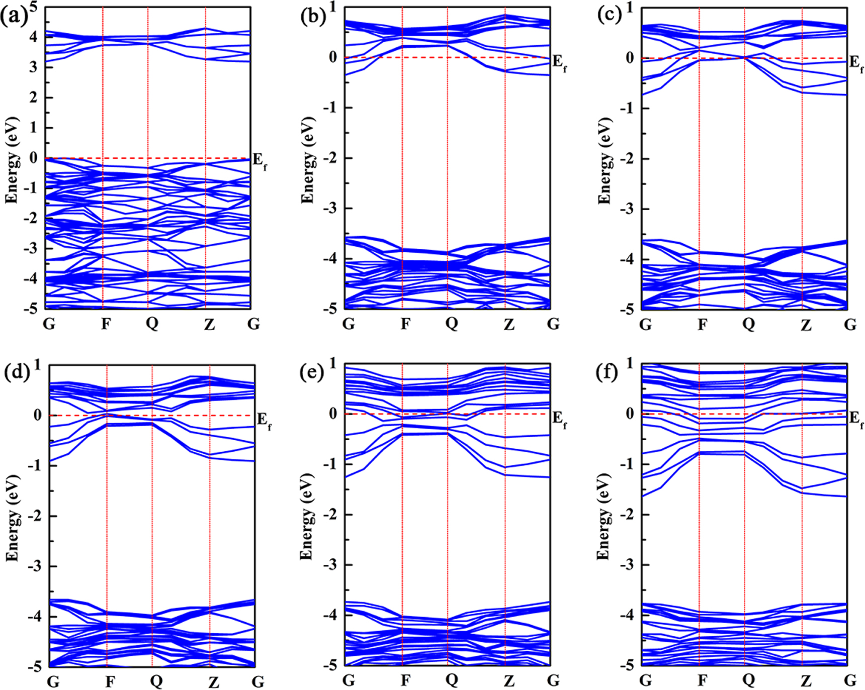
The calculated band structure of pure TiO2 is plotted in figure 4(a). It is found that the pure anatase TiO2 is a direct band gap semiconductor with a band gap of 3.197 eV at the G point, which is in good consistency with the experimental value of 3.2 eV. After Nb doping into the TiO2 lattice, no impurity level appears in the band gap of TiO2, but Fermi level enters into the conduction band, which shows a typical n-type metallic characteristic in electronic structure. With the increase of Nb concentration, Fermi level enters deeper into the conduction band, and the band gap value of TiO2 decreases gradually, but the optical band gap value increases from 3.197 eV to 3.771 eV of 14.58 at.% concentration, as shown in figures 4(b)–(f) and 6. The widening of the optical band gap can be explained by Burstein-Moss effect [35], which results from the Pauli exclusion principle. After the Fermi level enters the conduction band, all states below the Fermi level are occupied states. The electrons at the top of the valence band cannot be excited to enter these occupied states due to the restriction of Pauli exclusion principle, so they can only be excited to enter the conduction band above the Fermi level, and the absorption edge transfers to a higher level of energy, as a result the optical band gap widens.
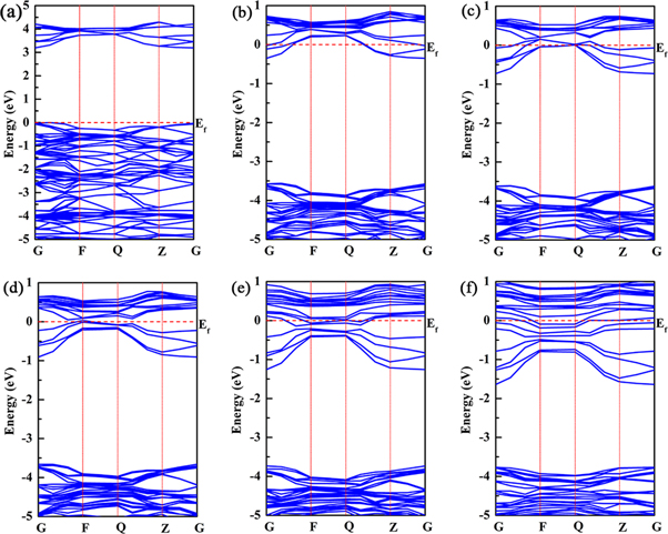
Figure 4. The band structures of TiO2 doped with Nb (a) 0 at. %, (b) 2.08 at.%, (c) 4.17 at.%, (d) 6.25 at.%, (e) 10.42 at.%, (f) 14.58 at.%.
Download figure:
Standard image High-resolution image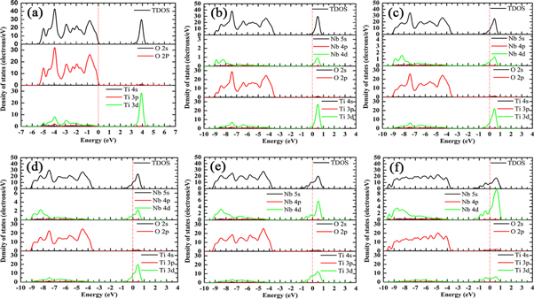
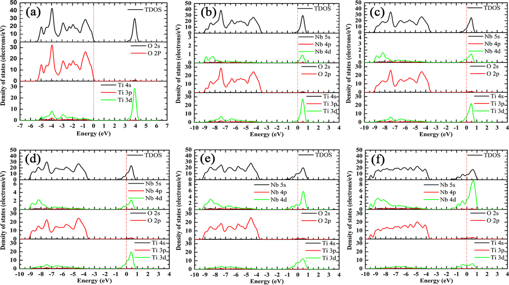
Figure 5. Density of states of TiO2 doped with Nb (a) 0 at.%, (b) 2.08 at.%, (c) 4.17 at.%, (d) 6.25 at.%,(e) 10.42 at.%, (f) 14.58 at.%.
Download figure:
Standard image High-resolution imageFigure 5 shows the total density of states (TDOS) and partial density of states (PDOS) of Nb-doped TiO2. In figure 5(a), the valence band of TiO2 mainly consists of O 2p and Ti 3d states, and the conduction band is mainly formed from Ti 3d, O 2p states. After the replacement of Ti atom by Nb atom, the occupied states at the bottom of the conduction band facilitate the Fermi level to enter the conduction band, and hybridization of Ti 3d, Nb 4d and O 2p states in the conduction band makes the bottom of the conduction band move towards the lower energy level, and the band gap value of Nb-doped TiO2 decreases from 3.197 eV to 1.91 eV, as shown in figures 5(b)–(f) and 6. By integrating the occupied states near Fermi level, the number of electrons entering the conduction band increases with the increase of Nb concentration, which means that the conductivity of Nb-doped TiO2 is enhanced. In the valence band, the overlap of Ti 3d, O 2p and Nb 4d states widens the valence band, and the number of electrons in the valence band also increases. The electrons can be excited to the conduction band through absorbing sufficiently high photon energy, which is another reason for the enhancement of conductivity. However, the conductivity of Nb-doped TiO2 does not always increase with the increase of Nb concentration. When Nb concentration is excessively high, the electronic states in the crystal will be modified by carrier-carrier and carrier-defect interactions, resulting in the scattering phenomenon [36, 37], which will reduce the hall mobility and deteriorate the conductivity. Therefore, Nb doping concentration needs to be controlled within a reasonable range considering the analysis of electrical and optical properties, which will be discussed in the later sections.
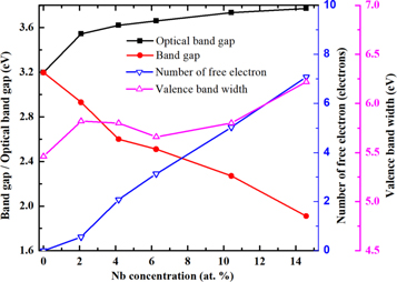
Figure 6. Optical band gap, band gap, free electrons near the bottom of the conduction band and valence band width for TiO2 with different concentrations of Nb.
Download figure:
Standard image High-resolution imageThrough the Mulliken population analysis, charge distribution and charge transfer of the material can be understood. In the pure TiO2 supercell, one Ti atom loss 1.33 electrons, one O atom nearby Ti atom accepts 0.67 electrons, as shown in table 2. With the increase of Nb concentration, the Mulliken populations of Ti and Nb decrease gradually, while the Mulliken population of O remains basically unchanged, indicating that the incorporation of Nb reduces the number of electrons transferred from Ti and Nb atoms to O atoms. The Mulliken populations of Nb are larger than that of Ti in the same Nb concentration, which means that Nb dopant contributes more electrons to the Nb-doped TiO2 supercell than Ti. The extra electrons are delocalized at the bottom of the conduction band and will lead to the transformation of Ti4+ to Ti3+ [14, 38]. In other words, the conductivity of the Nb-doped TiO2 is attributed to the presence of Ti3+ ions [39].
3.4. Electrical properties
Hall mobility, carrier concentration and conductivity have been three important parameters to characterize the electrical properties of TCO materials. Nb-doped anatase TiO2 exhibits the n-type conducting characteristics, which mainly depends on the free electrons for conduction. The electron mobility can be expressed by the following equation [40]:

Where q is the electronic charge,  is the relaxation time,
  is electron effective mass. The relaxation time
  is a function of ionized impurity concentration
  and thermodynamic temperature T:
  The electron effective mass
  can be obtained by calculating the average of the lateral and longitudinal effective masses in the Nb-doped TiO2 crystal structure, which is expressed by equation (3) [41].

Where  is the electron effective mass in the [100] direction,
  is the electron effective mass in the [001] direction. According to the band structure,
  and
and  at the bottom of the conduction band can be individually calculated by equation (4)) [42].

Where E(k) is the energy, k is the wave vector, ħ is the reduced Planck constant. According to equations (3) and (4), the effective mass of TiO2 doped with various Nb concentrations is showed in table 3. The electron effective masses along the [100] and [001] direction of TiO2 with Nb-doping concentration of 2.08 at.% are consistent with the experimental results of Hirose's research group [43]. They identified the electron effective mass along the a-axis ([100] direction) and the c-axis ([001] direction) as 0.2–0.6  and 0.5–3.3
  at low doping degrees, respectively. Taking TiO2 with Nb-doping concentration of 2.08 at. % as a benchmark, the relative mobility of TiO2 with other doping concentrations is calculated by equation (2), as displayed in table 3. The mobility reduces with the increasing Nb concentration, which is consistent with the previous experimental results [6, 37].
Table 3. Effective mass, electron concentration, mobility and conductivity of TiO2 doped with various concentrations of Nb.
| Nb concentration (at.%) | |||||
|---|---|---|---|---|---|
| 2.08 | 4.17 | 6.25 | 10.42 | 14.58 | |
Effective mass in the [100] direction,  ( ( ) ) | 0.226 | 0.546 | 0.359 | 0.384 | 0.768 |
Effective mass in the [001] direction,  ( ( ) ) | 1.809 | 2.764 | 4.983 | 1.861 | 5.157 |
Average effective mass,  ( ( ) ) | 0.319 | 0.745 | 0.520 | 0.522 | 1.072 |
Electron concentration,  (cm−3) (cm−3) | 9.91 × 10²⁰ | 3.65 × 10²¹ | 5.44 × 10²¹ | 8.59 × 10²¹ | 1.19 × 10²² |
Relative electron mobility, 
| 1 | 0.21 | 0.20 | 0.12 | 0.04 |
Relative conductivity, 
| 1 | 0.77 | 1.10 | 1.04 | 0.48 |
The electrons in Nb-doped TiO2 follow Fermi–Dirac distribution  which is expressed by the following equation (5):

Where  is the energy level at the base of the conduction band,
  is Fermi level,
  is Boltzmann constant, T is the thermodynamic temperature. The electron concentration
  in the conduction band can be calculated by equation (6).

Where V is the volume,  is the DOS near the Fermi level. In addition, the conductivity
  is a function of the electron concentration
  and the electron mobility

where q = 1.6 × 10⁻¹⁹ C is the elementary charge. According to equations (2)–(7), The electron concentration and the relative conductivity of Nb-doped TiO2 are both calculated, as shown in table 3. The calculated electron concentration value of 9.91 × 1020 cm−3 is in good agreement with experimentalvalue [44], and gradually increases to 1.19 × 1022 cm−3 with the increase of Nb-doping concentration. In the case of low Nb-doping (<6.25 at.%), the conductivity of Nb-doped TiO2 reduces slightly with the increase of Nb-doping concentration, which is also consistent with the experimental results [6]. When the doping concentration is 6.25 at.%, the conductivity will reach the maximum value and then slowly decreases. When the doping concentration reaches 14.58 at.%, the conductivity will rapidly decrease. The variation trend of conductivity at high Nb-doping accords well with the experimental results [37].
3.5. Optical properties
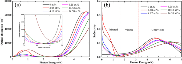
In order to understand the optical properties of TNO, the absorption spectra and reflectance spectra for the pure TiO2 and Nb-doped TiO2 were calculated respectively, as shown in figure 7. In the figure 7(a), the absorption edge of the pure TiO2 is near 3.2 eV, which shows that TiO2 is a direct band gap semiconductor. The absorption edge gradually shifts to the higher energy side as the Nb concentration increases, and appears blue-shift phenomenon. This is consistent with the results of previous experimental studies [45, 46]. The absorption spectra of Nb doping concentration in the range of 2.08 at.% to 10.42 at.% show an absorption peak near 0.7eV. When Nb concentration reaches 14.58 at.%, the absorption peak moves to the high energy level. The absorption intensity in the visible region increases. This is probably due to free electrons in the Ti 3d and Nb 4d orbitals in the conduction band. In the previous experiment, Kurita et al [47] prepared TiO2 films with different Nb-doping concentrations by PLD technique, and their absorption spectra showed similar results.
Figure 7. Calculation results of (a) absorption spectra and (b) reflectance spectra for the pure TiO2 and Nb-doped TiO2.
Download figure:
Standard image High-resolution image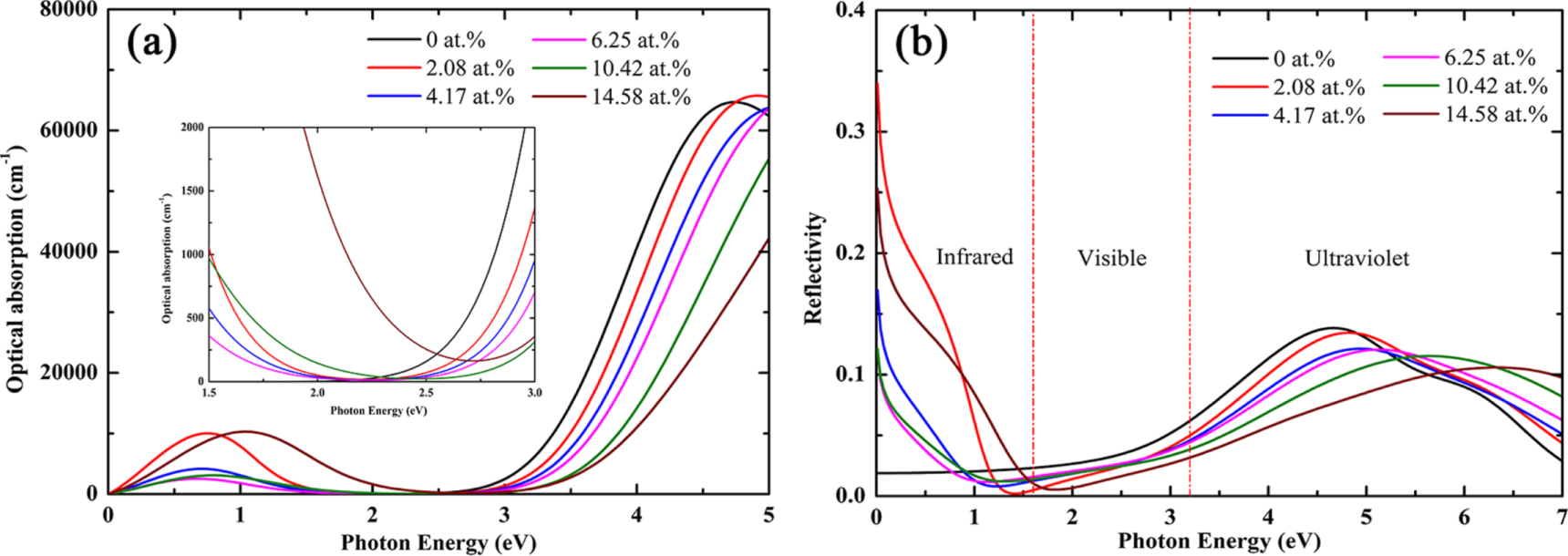
It can be seen from figure 7(b) that the reflectivity of doped TiO2 in visible region is lower than that of pure TiO2, but in infrared region, the reflectivity of doped TiO2 is much higher than that of pure TiO2. The reflectivity of doped TiO2 is below 10% in the visible region, which is better than that in infrared region and ultraviolet region, and the absorption coefficient is relatively low, which indicates that doped TiO2 possesses a relatively high transmittance in the visible region. However, when the concentration exceeds 14.58 at.%, the transmittance will deteriorate because of the larger absorption coefficient in the visible region.
4. Conclusions
This paper mainly investigated the effects of Nb concentration on Nb-doped anatase TiO2 via the GGA + U method based on the density functional theory. First of all, we studied the crystal structure and formation energies. The Nb atoms doped into the host lattice result in lattice distortion and the volume expansion slightly. The Nb-doped TiO2 system in O-rich environment is more stable than that in Ti-rich environment, and higher concentrations of Nb facilitate the synthesis of Nb-doped TiO2 systems. Secondly, the electronic structure of Nb-doped TiO2 is mainly transformed by the hybridization of Ti 3d, Nb 4d and O 2p states. The conductivity is enhanced due to the broadening of the valence band and occupied states at the bottom of the conduction band. With the increase of Nb concentration, the band gap decreases and optical band gap increase. Thirdly, the electrical properties of Nb-doped TiO2 are investigated. With the increase of Nb-doping concentration, electron concentration increases and electron mobility decreases. The conductivity reaches the maximum value at the high Nb-doping concentration of 6.25 at.%. Finally, the absorption spectra and reflectance spectra are analyzed. The absorption edge of Nb-doped TiO2 is found producing the blue shift. TiO2 with Nb-doping concentration less than 14.58 at.% exhibits the high transmittance in visible region. Our work can provide some theoretical basis for the preparation of TNO in the future.
Acknowledgments
The authors would like to acknowledge the support of the National Nature Science Foundation of China (Grant Number 61664010). The work was carried out at LvLiang Cloud Computing Center of China, and the calculations were performed on TianHe-2.
Data availability statement
All data that support the findings of this study are included within the article (and any supplementary files).