


Abstract
Anisotropic effect of two-dimensional materials remains one of the most attractive properties, introducing an additional degree of freedom for tuning physical performances. In this work, we investigate the anisotropies of electronic, transport, piezoelectric, and optoelectronic properties of Janus In2XY (X/Y = S, Se, Te) monolayers (J-In2XY MLs) by performing first-principles calculations. We find that such J-In2XY MLs possess moderate bandgap (2.07–2.29 eV), high carrier mobility (∼103 cm−2V−1s−1), visible light absorption (∼105 cm−1), large out-of-plane piezoelectric response  and ultra-soft mechanical nature
  . We construct a kind of J-In2XY-based phototransistor to investigate the optoelectronic properties under linearly polarized light. We find that the low recombination probability of photogenerated carriers ensured by anisotropic effect enhances the photocatalytic potential of J-In2XY MLs. And the pivotal role induced by anisotropy in photocurrent can cause a prominent on/off ratio (∼100), considerable responsivity (0.038 AW−1, 0.036 AW−1) and external quantum efficiency (10.6%, 11.5%). Our study provides an avenue for the design of future anisotropic J-In2XY-based multifunctional optoelectronic device.
Export citation and abstract BibTeX RIS

Original content from this work may be used under the terms of the Creative Commons Attribution 4.0 license. Any further distribution of this work must maintain attribution to the author(s) and the title of the work, journal citation and DOI.
1. Introduction
The changes in the band structure governed by quantum confinement effect determine that two-dimensional (2D) materials can exhibit differ greatly properties and phenomena from the parent compounds, which has been gradually confirmed since the graphene was successfully exfoliated in 2004 [1–3]. Apart from graphene, a decade of extensive research on various 2D layered materials has revealed their captivating characteristics and applied in many fields, such as field-effect transistors (FETs) [4–6], photodetectors [7–9], energy storage [10–12], sensing [13], and photovoltaic cells [14], etc.
Lately, an emerging class of van der Waals layered 2D semiconductors that belong to the III–VI chalcogenides combined by the formula MX (M = Ga, In; X = S, Se, Te), has drawn growing attention due to its extraordinary carrier mobility, excellent mechanical flexibility, superior light-matter interaction, and abundant polytypes [15–18]. Typically, the first member of monochalcogenides that is 2D InSe possesses tunable direct bandgap and can be synthesized by pulsed laser deposition [19], mechanical exfoliation [20], and chemical vapor deposition [21]. 2D InSe FET exhibits high intrinsic electron mobility of 103 cm2 (V s)−1 and superior Ion/Ioff ratio of 108 at room temperature [22]. Feng et al pronounced 2D InSe photodetectors showed a broadband photoresponse from ultraviolet (UV)–visible to near-infrared with the photoresponsivity of 104 AW−1 and photodetectivity of 1013 Jones [23]. In addition, 2D GaTe [24–28] and InTe [29, 30] with indirect bandgap (1.34 and 1.29 eV) have been proposed as one of the promising candidates for the next-generation electronic and optoelectronic devices. Moreover, for the group III–VI family, strikingly different from the aforementioned honeycomb-type hexagonal lattice structures, more complicated and lower symmetry monoclinic crystal with C2 m−1 space group can be obtained by choosing different growth patterns [25, 26], which exhibit strong anisotropic nonlinear optical properties and can be applied to phototransistors [24]. In particular, the anisotropic effects can add one more level of complexity and realize extraordinary nanodevice applications that are impossible for isotropic structures.
Breaking structural symmetry is an effective strategy to tune the electronic structure of 2D materials. For example, a J-MoSSe ML can be fabricated by fully replacing the top-layer S of ML MoS2 with Se [31]. This kind of Janus structures bring an additional degree of freedom and exhibit more fascinating characteristics than traditional transition metal dichalcogenides (TMDs), such as large vertical piezoelectric responses [32–36]. Interestingly, for the J-MXY (M= Ga, In; X/Y= S, Se, Te) MLs, some progresses show that their bandgaps are in the range of 0.89–2.03 eV, and possess in-plane piezoelectric coefficients up to 8.47 pm V−1, four times more than their binary counterpart MLs, and so on [37, 38]. However, few reports have uncovered that a single system based on J-MXY (M= Ga, In; X/Y= S, Se, Te) MLs can realize excellent multifunctional optoelectronic devices in terms of anisotropic effect.
In this work, we investigate J-In2 XY (X/Y = S, Se, Te) MLs to conduct their potential applications in terms of first-principles calculations. Firstly, we examine the dynamical, thermal, mechanical and energy stabilities of three configurations. Subsequently, we explore the electronic, mechanical, and optical anisotropic effects of J-In2 XY MLs. We find that J-In2 XY MLs possess excellent out-of-plane piezoelectric responses and flexibility, while the high and anisotropic carrier mobility and light absorption can promote the separation and transfer of photogenerated electrons and holes, ensuring high efficiency of photocatalytic reactions. Lastly, we explore direction-dependent optoelectronic properties of J-In2 XY p–n junctions, which show a large photocurrent on/off ratio, significant photo responsivities and external quantum efficiencies along the y direction of p–n junctions. Our study reveals the promising applications of J-In2 XY MLs as a multifunctional building block in optoelectronic devices.
2. Methodology
All first-principles calculations in this presentation are carried out with the Vienna ab initio simulation package (VASP) [39, 40] based on density functional theory (DFT) with the plane-wave basis projector augmented wave method [41]. The generalized gradient approximation (GGA) with Perdew–Burke–Ernzerhof (PBE) formalism is used for describing the exchange–correlation potential [42]. The plane-wave cutoff energy of  eV is applied to take into account the ion-electron interactions. The
  -centered
  k-point grids within the Monkhorst–Pack scheme are executed to sample the Brillouin zone in the self-consistent field calculations [43]. The geometric optimization can be terminated until the Hellmann–Feynman forces on each atom become smaller than 0.01 eV Å−1 and the energy difference between two sequential steps is less than 10−5 eV. The vacuum space of ∼20 Å is introduced along the c-axis to avoid artificial interactions between adjacent layers. Since PBE/GGA formalism systematically underestimates the electronic bandgap, the Heyd–Scuseria–Ernzerhorf (HSE06) hybrid functional is selected to provide a more accurate value for bandgap and band alignments. The dipole correction [44] along the c-axis is employed to handle inherent dipole moments as well as work functions. A
  supercell is selected to acquire the phonon dispersion relations by the small displacement method implemented in the PHONOPY package [45]. The thermal stability of J-In2
XY MLs is examined by performing ab initio molecular dynamics (AIMD) simulations during 144 atoms at 300 K with a total simulation time of 6 ps and time steps of 3 fs. The charge transfers between individual atoms are performed by using the Bader charge analysis technique [46]. The VASP within the density functional perturbation theory (DFPT) and small displacement methodology are carried out to obtain piezoelectric stress coefficients and linear-elastic properties, respectively.
supercell is selected to acquire the phonon dispersion relations by the small displacement method implemented in the PHONOPY package [45]. The thermal stability of J-In2
XY MLs is examined by performing ab initio molecular dynamics (AIMD) simulations during 144 atoms at 300 K with a total simulation time of 6 ps and time steps of 3 fs. The charge transfers between individual atoms are performed by using the Bader charge analysis technique [46]. The VASP within the density functional perturbation theory (DFPT) and small displacement methodology are carried out to obtain piezoelectric stress coefficients and linear-elastic properties, respectively.
The optical response is especially important relative to photocatalysis and photoelectric applications. The absorption coefficient  is calculated as the following formula [47]:

where c is the velocity of light, ω denotes the angular frequency of light,  and
and  refer to the real and imaginary parts of the dielectric function. The
  is calculated by using the Kramers–Kronig relation [47], and the
  of the frequency-dependent is determined based on the relation:

where the subscripts c and v represent the conduction and valence band states, respectively,  stand for the weight of the k-point; and
  denotes the cell periodic part of the orbitals at the k-point. Here, we mainly evaluate the maximum absorption coefficient and the overall optical properties. In order to save calculation cost, the optical properties under excitonic effect are not considered.
The quantum transport calculations of the optoelectronic FET are carried out using the QUANTUM Atomistix ToolKit [48] based on DFT and non-equilibrium Green's function (NEGF) [49]. The electron–photon interaction is considered in the Hamiltonian as  with
with  being the Hamiltonian without the electron-light interaction, and the
  represents the electron charge,
  denotes the free electron mass,
  and
and  are the momentum operator and the electromagnetic vector potential, respectively. The density mesh cut-off of 80 Hartree and 1 ×1 ×112 k-points mesh is adopted to the self-consistent calculation. The photocurrent in electrode
  with spin
  is calculated using first-order perturbation theory within the 1st Born approximation, as follows,

where  and
and  refer to the electron charge and reduced Planck's constant, and the effective transmission coefficients
  are obtained as [50]:

where  refer to the greater/lesser Green's function including electron–photon interactions, the
  and
and  stand for the linewidth and Fermi distribution function of the electrode (left or right), respectively.
3. Results and discussion
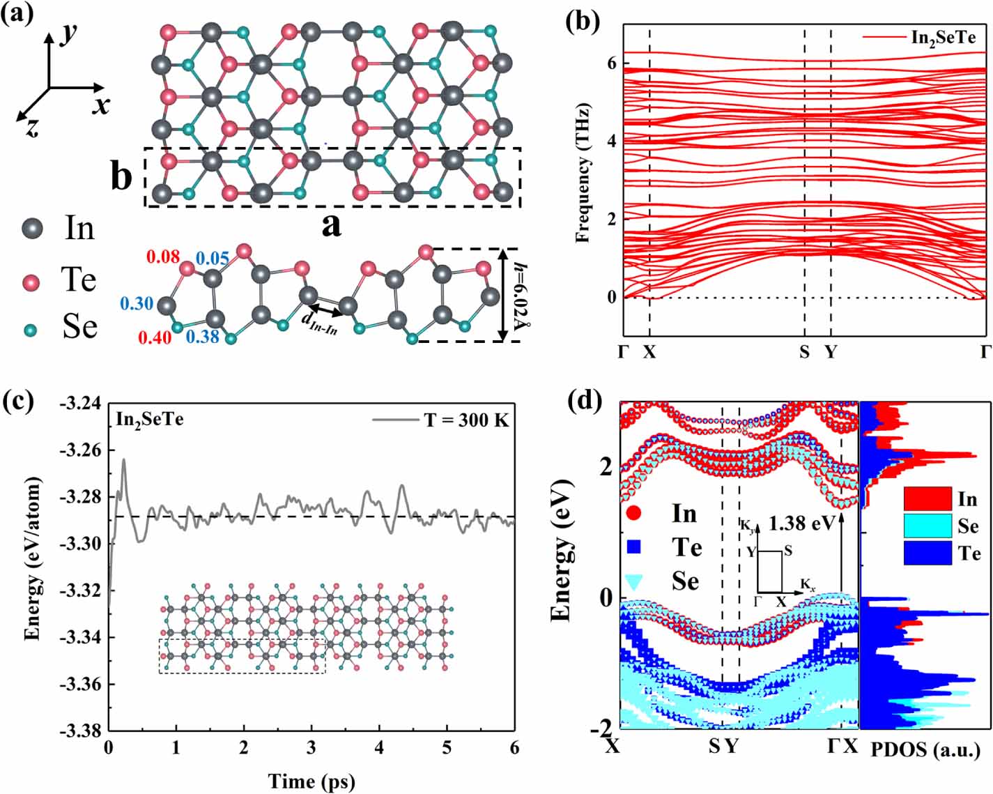
The structure of J-In2 XY MLs is designed by replacing the surface layer of InTe MLs with S and Se atoms. In contrast to its hexagonal lattice phase, the layered monoclinic phase with weak van der Waals interactions is more stable and possesses C2 m−1 space group with 2 m−1 point group symmetry. As illustrated in figure 1(a), the J-In2SeTe ML can be viewed as In atomic layer sandwiched between Te and Se atoms, and the rectangular unit cell consists of 12 indium, six selenium, and six tellurium atoms. The optimized lattice parameters of J-In2SeTe (a = 25.11 Å; b = 4.23 Å), J-In2STe (a = 24.59 Å; b = 4.15 Å) and J-In2SSe (a = 24.22 Å; b = 3.99 Å) MLs reveal in-plane anisotropy derived from the low symmetry introduced by the pseudo-one-dimensional structure. As listed in table 1, the bond lengths (dIn–In) of J-In2SeTe, J-In2STe, and J-In2SSe MLs are 2.83, 2.82 and 2.82 Å, the distance between upper and lower surface layers (h) are 6.02, 5.95 and 5.79 Å, respectively, which are very close to the previous results of the isomorphic system [18]. It should be noted that the difference of electronegativity between X and Y atoms leads to interfacial charge transfer and induces a large internal electric field (Eint). The Bader charge analysis confirms that Se and Te atoms obtain electrons and charge transfer is more favorable than Se atoms, as evident in figure 1(a).
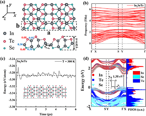
Figure 1. (a) Top and side views of J-In2SeTe ML. The unit cell is marked by a dashed black rectangle. Layer thickness and bond lengths are denoted by black arrows, and blue and red represent the accumulation and dissipation of electrons. (b) Phonon band dispersions of J-In2SeTe ML. (c) The variation of energy with respect to the time at 300 K for J-In2SeTe ML, the insets show the snapshots of atomic configurations at the end of AIMD simulations. (d) The atom-dependent projected electronic band structures and PDOS of J-In2SeTe ML.
Download figure:
Standard image High-resolution imageTable 1. Lattice constants a and b, corresponding bond lengths (dIn–In), ML thickness (h), cohesive energy (Ecoh), relaxed-ion elastic stiffness tensor elements ( ), energy bandgaps calculated within HSE06 (
 ) and GGA-PBE (
 ), and gap type (GT
).
), and gap type (GT
).
| In2 XY | a (Å) | b (Å) | dIn–In (Å) | H (Å) | Ecoh (eV) | C11 (N m−1) | C12 (N m−1) | C22 (N m−1) |
 (eV) (eV) |
 (eV) (eV) | GT |
|---|---|---|---|---|---|---|---|---|---|---|---|
| In2SeTe | 25.11 | 4.23 | 2.83 | 6.02 | −3.27 | 32.84 | 8.74 | 37.75 | 2.07 | 1.38 | direct |
| In2STe | 24.59 | 4.15 | 2.82 | 5.95 | −3.41 | 35.23 | 10.12 | 39.80 | 2.15 | 1.43 | direct |
| In2SSe | 24.22 | 3.99 | 2.82 | 5.79 | −3.60 | 35.90 | 10.56 | 43.41 | 2.29 | 1.54 | indirect |
To verify the structural stability of J-In2 XY MLs, the cohesive energy (Ecoh) per atom is calculated to quantitatively compare the energy stability as follows:

where  is the total energy of J-In2
XY ML unit cell, and
is the total energy of J-In2
XY ML unit cell, and  ,
,  and
and  stand for the single-atom energies of In, X and Y under vacuum, a, b and c represent the atom number of In, X and Y in the unit cell, respectively. From table 1, it is clearly seen that Ecoh of J-In2STe ML (−3.41 eV atom−1) is between those of J-In2SeTe (−3.27 eV atom−1) and J-In2SSe (−3.60 eV atom−1). To evaluate the dynamical stability, the phonon spectra of J-In2SeTe and J-In2SY (Y = Se, Te) MLs are calculated as depicted in figures 1(b) and S1 (supplemental materials). One can see that the phonon dispersions of J-In2
XY MLs are free from any imaginary frequencies through the whole Brillouin zone. Note that all phonon branches are both nondegenerate owing to the in-plane anisotropy that each J-In2
XY MLs possesses 69 optical phonon branches and three acoustic phonon branches. The thermal stability of both J-In2
XY MLs is predicted by carrying out AIMD simulations at 300 K for 6 ps, with a time step of 3 fs. Neither bond breaking nor structural reconstruction is observed in the resultant snapshot, and the total energy fluctuated around a fixed value without rising, as given in figures 1(c) and S1, implying that J-In2
XY MLs are thermal stability. Albeit the phonon spectra and AIMD simulations provide essential conditions, the mechanical stability of J-In2
XY MLs is also systematically examined. Such as the calculated elastic stiffness tensors of J-In2SeTe ML is
stand for the single-atom energies of In, X and Y under vacuum, a, b and c represent the atom number of In, X and Y in the unit cell, respectively. From table 1, it is clearly seen that Ecoh of J-In2STe ML (−3.41 eV atom−1) is between those of J-In2SeTe (−3.27 eV atom−1) and J-In2SSe (−3.60 eV atom−1). To evaluate the dynamical stability, the phonon spectra of J-In2SeTe and J-In2SY (Y = Se, Te) MLs are calculated as depicted in figures 1(b) and S1 (supplemental materials). One can see that the phonon dispersions of J-In2
XY MLs are free from any imaginary frequencies through the whole Brillouin zone. Note that all phonon branches are both nondegenerate owing to the in-plane anisotropy that each J-In2
XY MLs possesses 69 optical phonon branches and three acoustic phonon branches. The thermal stability of both J-In2
XY MLs is predicted by carrying out AIMD simulations at 300 K for 6 ps, with a time step of 3 fs. Neither bond breaking nor structural reconstruction is observed in the resultant snapshot, and the total energy fluctuated around a fixed value without rising, as given in figures 1(c) and S1, implying that J-In2
XY MLs are thermal stability. Albeit the phonon spectra and AIMD simulations provide essential conditions, the mechanical stability of J-In2
XY MLs is also systematically examined. Such as the calculated elastic stiffness tensors of J-In2SeTe ML is  ,
,  ,
,  and
and  N m−1, which satisfies the Born criteria [51] (
 and
and  ), as listed the table 1.
Figure 1(d) shows the atom-dependent projected band structure and projected density of states (PDOSs) of J-In2SeTe ML. Clearly, J-In2SeTe ML has a direct bandgap of 1.38 eV at the  point of Brillouin zone. The main contribution to the conduction-band minimum (CBM) comes from In atoms while that of In, Se and Te atoms to the valence-band maximum (VBM) is comparable. Besides, HSE06 hybrid functional is considered to provide a more accurate bandgap. The band structures of J-In2
XY MLs at the level of GGA/PBE and HSE06 are illustrated in figures 2(a)–(c). For the HSE06 algorithm, apart from J-In2SSe ML, which is predicted to be an indirect bandgap of 2.29 eV, J-In2SeTe and J-In2STe ML are obviously characterized by a direct bandgap semiconductor with a bandgap of 2.07 and 2.15 eV, respectively. Interestingly, the difference between the VBM of direct and indirect characteristics of J-In2
XY MLs is only ∼100 meV, hence the bandgap type (GT
) can be easily tuned by strain engineering [52]. Considering that the characteristics of band structures of J-In2
XY MLs are almost consistent based on the GGA/PBE and HSE06 algorithms, the effect of uniaxial strain along the x- and y- directions from −4% to 4% in the scheme of GGA/PBE on the band structures are investigated, and the indirect-direct band transition is given in figures 2(d) and (e). It is found that J-In2SSe ML is always an indirect bandgap semiconductor under x or y uniaxial strain, regardless of tensile or compressive strain. However, for J-In2SeTe ML, the bandgap transition from direct-to-indirect occurs at a tensile strain along the x direction, while that is just the opposite for J-In2STe ML. Unlike the uniaxial strain along the x direction, J-In2STe ML has an indirect bandgap under tensile strain along the y direction, and the bandgap transition from direct-to-indirect occurs from −1% to −2% for J-In2SeTe ML. In this case, strain engineering can be used to tune their electronic properties.
point of Brillouin zone. The main contribution to the conduction-band minimum (CBM) comes from In atoms while that of In, Se and Te atoms to the valence-band maximum (VBM) is comparable. Besides, HSE06 hybrid functional is considered to provide a more accurate bandgap. The band structures of J-In2
XY MLs at the level of GGA/PBE and HSE06 are illustrated in figures 2(a)–(c). For the HSE06 algorithm, apart from J-In2SSe ML, which is predicted to be an indirect bandgap of 2.29 eV, J-In2SeTe and J-In2STe ML are obviously characterized by a direct bandgap semiconductor with a bandgap of 2.07 and 2.15 eV, respectively. Interestingly, the difference between the VBM of direct and indirect characteristics of J-In2
XY MLs is only ∼100 meV, hence the bandgap type (GT
) can be easily tuned by strain engineering [52]. Considering that the characteristics of band structures of J-In2
XY MLs are almost consistent based on the GGA/PBE and HSE06 algorithms, the effect of uniaxial strain along the x- and y- directions from −4% to 4% in the scheme of GGA/PBE on the band structures are investigated, and the indirect-direct band transition is given in figures 2(d) and (e). It is found that J-In2SSe ML is always an indirect bandgap semiconductor under x or y uniaxial strain, regardless of tensile or compressive strain. However, for J-In2SeTe ML, the bandgap transition from direct-to-indirect occurs at a tensile strain along the x direction, while that is just the opposite for J-In2STe ML. Unlike the uniaxial strain along the x direction, J-In2STe ML has an indirect bandgap under tensile strain along the y direction, and the bandgap transition from direct-to-indirect occurs from −1% to −2% for J-In2SeTe ML. In this case, strain engineering can be used to tune their electronic properties.
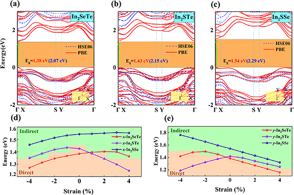
Figure 2. (a)–(c) The electronic band structures of J-In2 XY MLs within the framework of DFT-PBE and HSE06. The Fermi level is set to zero. Bandgaps of J-In2 XY MLs under uniaxial strain (d) x and (e) y from −4% to +4%. Positive (negative) numbers refer to tensile (compressive) strain. The green area (labeled by 'Indirect') refers to the indirect bandgap, while the orange area (marked with 'Direct') stands for the direct bandgap.
Download figure:
Standard image High-resolution imagePiezoelectricity in layered material with interlayer van der Waals interactions has received considerable interest as the energy conversion bridges between mechanical and electrical energies. However, the piezoelectric response of most 2D layered materials is confined to exist only at the basal plane, which limits the operation of piezoelectric devices [32]. Here J-In2
XY MLs are purposed to exhibit an additional piezoelectric degree of freedom arising from the out-of-plane symmetry breaking in which an electric dipole moment is generated. Theoretically, the piezoelectric response can be characterized by the relaxed-ion piezoelectric stress tensor  and piezoelectric strain tensor
  , which is combined the contributions from ionics and electronics. Based on the Voigt notation, the
  and
and  can be connected by elastic stiffness tensor
  , i.e.
  .
.
The piezoelectric anisotropy of in-plane and out-of-plane is also taken into account, thus there are four non-zero elements of  for the rectangle supercell J-In2
XY MLs, i.e.
for the rectangle supercell J-In2
XY MLs, i.e.  ,
,  ,
,  and
and  , where
  represents the direction being polarized,
  denotes the direction in which the strain is applied, and numbers 1, 2 and 3 stand for x, y, and out-of-plane directions, respectively. Therefore, we have the relations:

 and
and  where
where  is calculated by using small displacement methodology, as listed in table 1. Also, the orientation-dependent Young's moduli
  , Poisson's ratios
  , and shear moduli
  are obtained as given in figures S2 and S3. Evidently, J-In2
XY MLs exhibit different elastic properties depending on the angle because of anisotropy. Notably, the Young's moduli of J-In2
XY MLs range from 25.72 to 40.62 N m−1, which are much smaller than those of other 2D layered materials, such as MoS2 (122 N m−1) and graphene (330 N m−1) [53], indicating their ultra-soft natures. Subsequently,
are obtained as given in figures S2 and S3. Evidently, J-In2
XY MLs exhibit different elastic properties depending on the angle because of anisotropy. Notably, the Young's moduli of J-In2
XY MLs range from 25.72 to 40.62 N m−1, which are much smaller than those of other 2D layered materials, such as MoS2 (122 N m−1) and graphene (330 N m−1) [53], indicating their ultra-soft natures. Subsequently,  and
and  are calculated via DFPT as depicted in figure 3. The anisotropy of piezoelectricity can be found both in- (
 and
and  ) and out-of-plane (
 and
and  ). Note that
  of J-In2STe ML is 0 because the contributions of ionics and electronics cancel out each other. In addition,
  and
and  are 2.88 and 5.98 pm V−1 for J-In2STe ML, in which the values are comparable to that of J-MoSSe ML (
 =
=  = 3.76 pm V−1) [53]. More significantly, a large out-of-plane piezoelectric response and anisotropy are obtained when strained transverse to the basal plane. Among the MLs we studied,
  and
and  of 0.42 and 0.34 pm V−1 are the most favorable for J-In2SeTe ML, which is larger by one order of magnitude compared to J-TMDs (0.007–0.030 pm V−1) [32]. This will greatly increase their flexibility and compatibility with existing device operations.
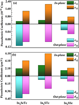
Figure 3. For the J-In2 XY MLs, (a) the relaxed-ion piezoelectric stress coefficients along in-plane e11, e12 and out-of-plane e31, e32 (unit: 10−10 C m−1). (b) The piezoelectric strain coefficients along in-plane d11, d12 and out-of-plane d31, d32 (unit: pm V−1).
Download figure:
Standard image High-resolution imageMoreover, we consider the net dipole moments of J-In2
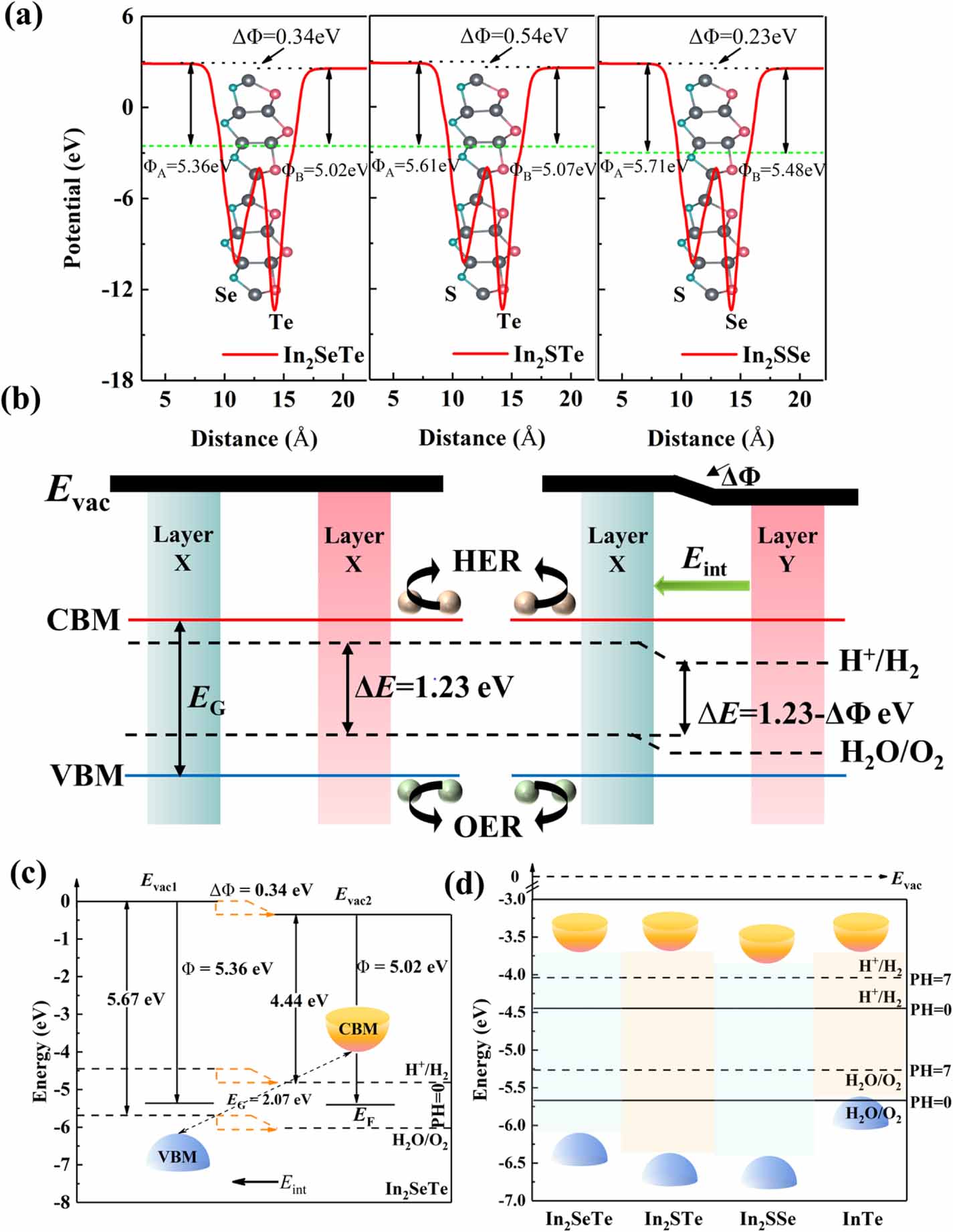
XY MLs along the out-of-plane direction to compare the out-of-plane polarization responses. The net dipole moments along the out-of-plane direction, namely z-direction, are calculated to be 0.18, 0.29 and 0.11 eÅ for J-In2SeTe, J-In2STe and J-In2SSe MLs, respectively. Interestingly, the vacuum energy level of the surface layer can be regulated by the net dipole moment of the Janus structures, which leads to the difference of electrostatic potential energy. In figure 4(a), the discrepancies between two surface layers are 0.34, 0.54 and 0.23 eV, respectively, which allow the oxidation or reduction potential of water splitting to shift downward and better serve photocatalysis, a new reaction mechanism of efficient photocatalysis was first proposed by Li et al [33]. To make it clear, the traditional and the new mechanism illustrations for photocatalytic water splitting are depicted in the left and right sections of figure 4(b). For the former, the standard reduction potential for hydrogen evolution reaction (HER) is −4.44 eV, while that of the oxidation potential for oxygen evolution reaction (OER) is −5.67 eV. Therefore, the bandgap of photocatalytic materials is not less than 1.23 eV, which is necessary to ensure HER and OER. However, for the latter, the internal electric field induced by the out-of-plane polarization bends the vacuum level of layer Y downward by  , while the oxidation/reduction potential is still −5.67/−4.44 relative to the vacuum level of layer X/Y, thus the limitation of the bandgap for photocatalytic materials is redefined as
  eV.
eV.
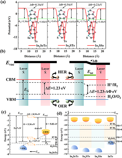
Figure 4. (a) Effective potential profiles of J-In2 XY MLs under dipole correction. (b) The mechanism on the photocatalysis of the traditional and Janus structure. The gold and cyan balls correspond to electrons and holes, which are involved in the HER and OERs, respectively. The Eint represents the direction of the internal electric field. Band alignments with regard to the vacuum level of (c) J-In2SeTe and (d) J-In2 XY and InTe MLs under the approach of HSE06 functional.
Download figure:
Standard image High-resolution imageAlthough numerous semiconductors satisfy the bandgap criterion, their band alignments are not viable for the two half-reactions standard potential of water splitting (2 H+(aq) + 2e− → H2(g), H2O → 2 H+ + 1/2O2). To test the mentioned requirements for oxidation/reduction potential and further clarify the mechanism of photocatalytic water splitting, the band-edge positions of J-In2SeTe ML calculated by HSE06 are aligned concerning the vacuum level, as illustrated in figure 4(c). Clearly, the work functions ( ) of Se and Te layers induced by polarization are 5.36 and 5.02 eV, respectively, resulting in the corresponding HER potential (−4.44 eV) relative to the CBM (−3.96 eV) moved down by 0.34 eV. Thus, the J-In2SeTe ML is predicted to exhibit the excellent photocatalytic capacity for hydrogen production by water splitting owing to the CBM has greatly exceeded the standard reduction potential (
 ). More interesting, the Eint directed by Te to Se can accelerate efficient spatial separation and transfer of photogenerated carriers and suppress their recombination, which facilitates for HER and OER. Also, we evaluate the band-edge position of relative vacuum levels of J-In2STe and J-In2SSe MLs as well as the corresponding binary parent structure InTe ML, as displayed in figure 4(d). Evidently, the band-edge positions of J-In2
XY MLs straddle the standard redox potentials of water in strongly acidic (pH = 0) conditions. Note that qualified photocatalytic material should still be suitable over a wide pH range, and the standard potential of both
). More interesting, the Eint directed by Te to Se can accelerate efficient spatial separation and transfer of photogenerated carriers and suppress their recombination, which facilitates for HER and OER. Also, we evaluate the band-edge position of relative vacuum levels of J-In2STe and J-In2SSe MLs as well as the corresponding binary parent structure InTe ML, as displayed in figure 4(d). Evidently, the band-edge positions of J-In2
XY MLs straddle the standard redox potentials of water in strongly acidic (pH = 0) conditions. Note that qualified photocatalytic material should still be suitable over a wide pH range, and the standard potential of both  and
and  sensitively varies with PH according to the Nernst equations [54]:
  and
and  . As evident in figure 4(d), the CBM and VBM of J-In2
XY MLs completely straddle both the potential of HER and OER in strongly acidic (pH = 0) and neutral (pH = 7) environments. However, the corresponding binary InTe ML is incapable of covering the potential of OER under pH = 0, indicating that J-In2
XY MLs exhibit more superior photocatalytic ability for overall water splitting than the corresponding binary parent materials under extreme conditions.
. As evident in figure 4(d), the CBM and VBM of J-In2
XY MLs completely straddle both the potential of HER and OER in strongly acidic (pH = 0) and neutral (pH = 7) environments. However, the corresponding binary InTe ML is incapable of covering the potential of OER under pH = 0, indicating that J-In2
XY MLs exhibit more superior photocatalytic ability for overall water splitting than the corresponding binary parent materials under extreme conditions.
A promising photocatalytic material should possess high carrier mobility in addition to the two criteria investigated above, which facilitate the rapid transfer of electrons and holes into HER and OER before recombination. Therefore, we address the carrier mobility of J-In2
XY MLs along x-and y-directions using the deformation potential theory [55],  where
where  refers to the average effective mass (i = e for electrons, i = h for holes, and x and y are the transport directions), The effective mass of electrons and holes is:
 ![$m_{i(x/y)}^* = {\hbar ^2}{\left[ {{\partial ^2}E(k)/\partial {k^2}} \right]^{ - 1}}$](https://content.cld.iop.org/journals/1367-2630/25/8/083013/revision2/njpace845ieqn88.gif) , and
, and  stands for the corresponding elastic constant of the 2D system,
  and
and  are the total energy shift and the area of initial unit cell,
  and
and  denote the Boltzmann constant and Planck constant, room temperature
  is used,
  is the deformation potential, and
  is the band edge drift of CBM for electrons and VBM for holes under uniaxial x or y strain. The evaluated values are summarized in table 2 and the corresponding fitting details are given in the supplemental materials (figure S4). Clearly, all the MLs exhibit outstanding carrier mobility, where the electron mobility of J-In2SSe ML along the x-direction amounts to
  and the hole in the y-direction is
  , is one order of magnitude higher than the theoretically evaluated for MoS2 ML (
 and
and  for electron and hole mobilities, respectively) [56]. Moreover, it is found that the electron and hole mobilities of J-In2
XY MLs are significantly discrepancy, which may enhance electron-hole separation efficiency and photocatalytic activity [57].
for electron and hole mobilities, respectively) [56]. Moreover, it is found that the electron and hole mobilities of J-In2
XY MLs are significantly discrepancy, which may enhance electron-hole separation efficiency and photocatalytic activity [57].
Table 2. Effective mass mx
* (my
*), deformation potential E1x
(E1y
), 2D elastic modulus C2Dx
(C2Dy
), and carrier mobility μx
(μy
) of J-In2
XY MLs along  -X (
-X ( -Y) directions for electron (e) and hole (h).
| In2 XY | mx * (m0) | my * (m0) | E1x (eV) | E1y (eV) | C2Dx (J m−2) | C2Dy (J m−2) | μx (cm−2V−1s−1) | μy (cm−2V−1s−1) | |
|---|---|---|---|---|---|---|---|---|---|
| In2SeTe | e | 0.30 | 0.25 | 2.20 | 4.75 | 30.26 | 34.99 | 1460.41 | 434.72 |
| h | 0.26 | 5.84 | 3.62 | 0.92 | 30.26 | 34.99 | 138.63 | 110.51 | |
| In2STe | e | 0.36 | 0.27 | 1.99 | 4.21 | 32.29 | 36.75 | 1393.61 | 472.42 |
| h | 1.96 | 0.91 | 2.07 | 0.87 | 32.29 | 36.75 | 55.06 | 769.99 | |
| In2SSe | e | 0.52 | 0.28 | 0.86 | 3.43 | 34.66 | 40.19 | 4533.94 | 1608.44 |
| h | 1.44 | 3.76 | 1.72 | 2.17 | 34.66 | 40.19 | 67.12 | 18.73 |
What's more, the carrier mobilities of J-In2
XY MLs show strong in-plane directional anisotropy. For instance, the electron mobility of J-In2SeTe ML along the x-direction is  , much higher than that (
 ) in the y-direction, and the anisotropic ratio
 ![$[\max ({\mu _x},{\mu _y})/\min ({\mu _x},{\mu _y})]$](https://content.cld.iop.org/journals/1367-2630/25/8/083013/revision2/njpace845ieqn105.gif) of electron mobility is about 3.36, which is comparable to the cases of SiAs ML (4.03) [58] and 2D ReS2 sheet (3.1) [59]. To more intuitively reflect the anisotropy of electronic structure and carrier mobility, the three-dimensional valleys for VBM and CBM of J-In2SeTe ML are depicted in figure 5(a), and the corresponding 2D contour view is given in figures 5(b) and (c). Clearly, the valleys of VBM and CBM both show different dispersion profiles in the
of electron mobility is about 3.36, which is comparable to the cases of SiAs ML (4.03) [58] and 2D ReS2 sheet (3.1) [59]. To more intuitively reflect the anisotropy of electronic structure and carrier mobility, the three-dimensional valleys for VBM and CBM of J-In2SeTe ML are depicted in figure 5(a), and the corresponding 2D contour view is given in figures 5(b) and (c). Clearly, the valleys of VBM and CBM both show different dispersion profiles in the  and
and  , respectively, which can induce a high degree of anisotropy of electronic properties. Furthermore, we fit the quadratic function curve of the energy with respect to the
  and
and  in the near
  point (see figures 5(d) and (e)). The trend of the curve is consistent with the effective mass approximation, and by unit conversion, the carrier effective mass (
 ) and quadratic coefficient (
 ) can be defined as
  , the details of calculation are shown in the supplemental materials. For the case of J-In2SeTe ML, the presence of electron effective mass in the x-direction is
  , and
, and  for the y-direction, while the hole effective mass along the x-direction (
 ) is much smaller than that along the y-direction (
 ). In that sense, the high carrier mobility with strong in-plane anisotropy can effectively inhibit the recombination of free electrons and holes [60, 61], which can improve the overall efficiency of photocatalytic water splitting.
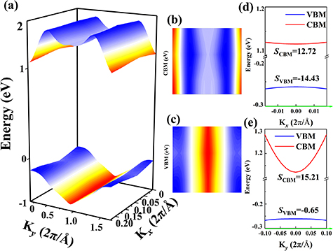
Figure 5. (a) Surface plot of valleys around the CBM and VBM for the J-In2SeTe ML. (b) and (c) Two-dimensional contour views of CBM and VBM. (d) and (e) Band dispersion around the  point along the kx
and ky
directions.
point along the kx
and ky
directions.  and
and  are the coefficients of the quadratic function fitted near the CBM and VBM, respectively. The carrier effective mass is defined as:
  .
.
Download figure:
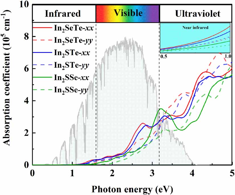
Standard image High-resolution imageAdditionally, the absorption capacity of solar light is an important indicator to confirm the efficiency of photocatalysis, and also plays a crucial role in the field of photovoltaic devices. In our case, the optical responses of J-In2
XY MLs are examined by computing their frequency-dependent dielectric functions and absorption coefficients ![$[\alpha (\omega )]$](https://content.cld.iop.org/journals/1367-2630/25/8/083013/revision2/njpace845ieqn122.gif) . The imaginary part of the dielectric function
. The imaginary part of the dielectric function  and
and ![$[\alpha (\omega )]$](https://content.cld.iop.org/journals/1367-2630/25/8/083013/revision2/njpace845ieqn124.gif) versus the energy of the incident light polarization along
versus the energy of the incident light polarization along  and
and  directions are depicted in figures S5 and 6, respectively. Notably, the significant optical anisotropy can be directly observed in the visible to UV region, and the zoomed-in image around 0.5–1 eV shows that there is still anisotropy in the near-infrared region because of their low lattice symmetry, in which the absorption intensity along the
  direction is higher than that in the
  direction in the near-infrared to visible light region for all J-In2
XY MLs. Moreover, the absorption spectrum of J-In2
XY MLs overlaps massively under the incident AM1.5 solar flux in the visible region, and the first conspicuous absorption peak also occurs in this area, it is evident that J-In2
XY MLs are sensitive to the absorption response in the visible range. The broad optical absorption range with high absorption coefficients (105 cm−1) are comparable to the perovskites that are known to be highly efficient for solar cells [62]. The large absorption coefficients combining the significant optical anisotropy in the visible region can support its superior properties in terms of water-splitting reactions and optoelectronic applications.
direction in the near-infrared to visible light region for all J-In2
XY MLs. Moreover, the absorption spectrum of J-In2
XY MLs overlaps massively under the incident AM1.5 solar flux in the visible region, and the first conspicuous absorption peak also occurs in this area, it is evident that J-In2
XY MLs are sensitive to the absorption response in the visible range. The broad optical absorption range with high absorption coefficients (105 cm−1) are comparable to the perovskites that are known to be highly efficient for solar cells [62]. The large absorption coefficients combining the significant optical anisotropy in the visible region can support its superior properties in terms of water-splitting reactions and optoelectronic applications.
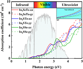
Figure 6. Optical absorption coefficient as a function of photon energy for J-In2 XY MLs to the light incident along the in-plane x and y polarization. The background is the reference of the solar spectral irradiance at AM1.5. The inset in the upper right corner is a magnified view of the absorption coefficients in the near-infrared region range between 0.5 and 1 eV.
Download figure:
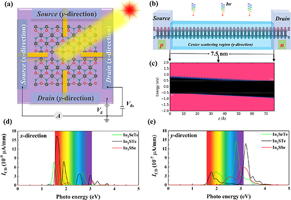
Standard image High-resolution imageTo further explore the potential applications of J-In2
XY MLs in optoelectronic devices based on their excellent optical properties, we construct an abrupt-change J-In2
XY ML p–n junction phototransistor to investigate the photocurrent along the two main directions. Noticeably, the top view of the schematic diagram is illustrated in figure 7(a), and the side view along the y-direction is given in figure 7(b). The p–n junctions along the transport directions (x and y) with two-probed devices consisting of two semi-infinite electrodes sandwiched a central scattering region. The lengths of the central scattering region in the x- and y-directions are both about 7.5 nm. The source (S) and drain (D) electrodes are doped with p- and n-type concentrations of 1019e cm−3, which similar doping level is commonly applied in 2D-based FET simulations [63, 64] and experimentally possible [65, 66]. An external bias voltage Vds = 1.0 V with both relative permittivity and relative permeability set to 1 is applied to drive the photo-generated carriers, and the photon-generated current under the linearly polarized light radiation is obtained by using AM1.5 standard solar spectrum with that of photon flux  in the 300 K. The local density of states (LDOS) of J-In2
XY p–n junctions along the y-direction are illustrated in figure 7(c), A typical p–n profile can be clearly seen along the device, and there is a 1.0 V potential difference between S and D electrodes. The width of the black area refers to the bandgap of the electrode material, which is very close to the results mentioned above. Furthermore, the flat band near the S/D electrode represents the converged screening built-in potential that provides a drift field for the photoexcited carrier.
in the 300 K. The local density of states (LDOS) of J-In2
XY p–n junctions along the y-direction are illustrated in figure 7(c), A typical p–n profile can be clearly seen along the device, and there is a 1.0 V potential difference between S and D electrodes. The width of the black area refers to the bandgap of the electrode material, which is very close to the results mentioned above. Furthermore, the flat band near the S/D electrode represents the converged screening built-in potential that provides a drift field for the photoexcited carrier.
Figure 7. (a) A schematic diagram of direction-dependent J-In2 XY MLs optoelectronic FET. (b) and (c) The device configuration and corresponding LDOS (Vds = 1.0 V) in the y-direction on a logarithmic scale. (d) and (e) Photocurrent density as a function of photon energy in the x- and y-directions.
Download figure:
Standard image High-resolution image
The direction-dependent photogenerated current density ( ) is calculated for testing the polarization sensitivity based on the electron–phonon coupling within the DFT +NEGF formalism. As shown in figures 7(d) and (e), the peaks of
  for the p–n junctions are in the visible and near UV regions, the maxima are at the level of 10−9
μA mm−1 in the x-direction and 10−7
μA mm−1 in the y-direction. It manifests that the p–n junctions are prominent photoelectric anisotropy and result in a high on/off ratio, the measured ratio is ∼100 according to the formula
for the p–n junctions are in the visible and near UV regions, the maxima are at the level of 10−9
μA mm−1 in the x-direction and 10−7
μA mm−1 in the y-direction. It manifests that the p–n junctions are prominent photoelectric anisotropy and result in a high on/off ratio, the measured ratio is ∼100 according to the formula ![$[\max ({I_{{\text{CD}}x}},{I_{{\text{CD}}y}})/\min ({I_{{\text{CD}}x}},{I_{{\text{CD}}y}})]$](https://content.cld.iop.org/journals/1367-2630/25/8/083013/revision2/njpace845ieqn132.gif) . Furthermore, the
. Furthermore, the  of J-In2SeTe ML along y-direction is 14.41 ×10⁻⁷
μA mm−1, which is higher than those of SbBi ML optoelectronic FET [67]. Note the frontier molecular orbitals of the electrode and the center scattering region do not produce resonance peaks at 4 and 5 eV, the photo-excited carriers are localized, resulting in very small photocurrents. To characterize the energy conversion efficiency, the photo responsivity (
of J-In2SeTe ML along y-direction is 14.41 ×10⁻⁷
μA mm−1, which is higher than those of SbBi ML optoelectronic FET [67]. Note the frontier molecular orbitals of the electrode and the center scattering region do not produce resonance peaks at 4 and 5 eV, the photo-excited carriers are localized, resulting in very small photocurrents. To characterize the energy conversion efficiency, the photo responsivity ( ) is a critical indicator that is defined as:
  where
where  and
and  refer to the photocurrent and effective illumination area,
  represents the incident photon power density. The obtained
  of J-In2SeTe, J-In2STe and J-In2SSe MLs in the y-direction are 0.038, 0.036 and 0.015 AW−1, respectively. Which is close to that SbBi (0.089 AW−1) [67], black phosphorus (0.0648 AW−1) [68], and higher than those of MoS2 (0.016 AW−1) [66]. Moreover, the external quantum efficiency (
 ) is
) is  where
where  and
and  are the Planck's constant and the speed of light,
  and
and  denote the electron charge and the wavelength of incident light, respectively. The calculated peaks of
  in J-In2SeTe, J-In2STe and J-In2SSe MLs are 10.6%, 11.5% and 4.7%. Therefore, the results of high
  and
and  combined anisotropic photoelectric response further confirm that J-In2
XY MLs can be suitable for the potential applications in multifunctional optoelectronic devices.
combined anisotropic photoelectric response further confirm that J-In2
XY MLs can be suitable for the potential applications in multifunctional optoelectronic devices.
4. Conclusions
In summary, we investigate J-In2
XY MLs with low symmetry as a promising multifunctional candidate for overall photocatalytic water splitting and flexible optoelectronic nanodevices. The anisotropy of electronic, piezoelectric, transport, and photoelectric properties are systematically explored by using first-principles calculations with the framework of DFT + NEGF. The favorable stability of J-In2
XY MLs are confirmed by phonon dispersions, cohesive energies and AIMD simulations. Three types of stable structures are both flexible semiconductors with moderate bandgaps. The positions of valence and conduction-band edges are adequate for OER and HER over a wide PH range (from 0 to 7), owing to internal electric field with the direction of the Y layer pointing to the X layer caused by the out-of-plane polarization. The J-In2
XY MLs with large out-of-plane polarization could be conducive to facilitating the efficient separation and transfer of photogenerated carriers. Moreover, the out-of-plane piezoelectric coefficient of J-In2SeTe ML  is larger by one order of magnitude compared to the J-TMDs. More importantly, highly anisotropic carrier mobility (more than 103 cm−2V−1s−1 along the x-direction, and 102 cm−2V−1s−1 in the y-direction) and visible light absorption (approximately 105 cm−1) herald notable performance of the overall photocatalysis. Moreover, the direction-dependent p–n junction based on J-In2
XY MLs exhibits considerable photocurrent on/off ratios (∼100). Our results of anisotropic piezoelectric, transport and photoelectric together with suitable band edges for the novel J-In2
XY MLs suggest that they exhibit attractive prospects for the design of multifunctional optoelectronic devices.
is larger by one order of magnitude compared to the J-TMDs. More importantly, highly anisotropic carrier mobility (more than 103 cm−2V−1s−1 along the x-direction, and 102 cm−2V−1s−1 in the y-direction) and visible light absorption (approximately 105 cm−1) herald notable performance of the overall photocatalysis. Moreover, the direction-dependent p–n junction based on J-In2
XY MLs exhibits considerable photocurrent on/off ratios (∼100). Our results of anisotropic piezoelectric, transport and photoelectric together with suitable band edges for the novel J-In2
XY MLs suggest that they exhibit attractive prospects for the design of multifunctional optoelectronic devices.
Acknowledgments
This work was supported by the National Natural Science Foundation of China (Grant No. U2001215), and Postgraduate Scientific Research Innovation Project of Hunan Province (CX20230514).
Data availability statement
All data that support the findings of this study are included within the article (and any supplementary files).
Supplementary data (3.0 MB DOCX)