


Abstract
We have fabricated and characterized a Landau level spin diode in a GaAs two-dimensional hole system. We used the spin diode to probe the hyperfine coupling between hole and nuclear spins and found no detectable net nuclear spin polarization, indicating that hole–nuclear spin flip-flop processes are suppressed by at least factor of 50 compared to GaAs electron systems.
Export citation and abstract BibTeX RIS

Content from this work may be used under the terms of the Creative Commons Attribution 3.0 licence. Any further distribution of this work must maintain attribution to the author(s) and the title of the work, journal citation and DOI.
Studying the coupling between the spins of charge carriers and nuclear spins is a rapidly expanding field due to application of spin qubits in quantum information processing [1]. This coupling is a major source of electron spin decoherence in GaAs spin qubits, because both Ga and As have nonzero nuclear spins. Several approaches have been developed to suppress this unwanted interaction [1, 2], including NMR techniques such as spin-echo, dynamic nuclear polarization as well as the elimination of nuclear spins by using nuclear-spin free materials such as 12C or 28Si. An alternative approach to minimizing spin decoherence is to use hole spins since hyperfine coupling is much weaker than for electrons [3]. The contact hyperfine interaction between an electron spin S and nuclear spins I is given by [4]:  , where
  . The first 'flip-flop' term describes a process where the electron spin changes its orientation, and the nuclear spin simultaneously changes its orientation in the opposite direction. The second term describes the influence of nuclear polarization on the electrons via the effective Overhauser magnetic field. Valence band holes are formed by p-type atomic orbitals and so have zero overlap with the nuclei, unlike conduction band electrons which come from s-type orbitals. This eliminates the contact hyperfine interaction leaving only the weaker dipolar hyperfine interaction. For light holes (LH) the nuclear spin coupling takes a similar form to that for electrons [5]:
 ![${{H}_{{\rm LH},n}}=\frac{{{M}_{P}}}{3}[({{I}_{+}}{{S}_{-}}+{{I}_{-}}{{S}_{+}})+{{I}_{Z}}{{S}_{Z}}]$](https://content.cld.iop.org/journals/1367-2630/17/3/033035/revision1/njp510395ieqn3.gif) , where
, where  , but MP is almost an order of magnitude smaller than MS [6]. For pure heavy holes (HH) there is no spin-flip flop term [5], with only the Overhauser term present:
  .
.
Although there have been some electrical studies of the hyperfine coupling for holes in GaAs [7], most studies have probed holes optically in self-assembled quantum dots [8, 9]. The optical studies have confirmed theoretical predictions that the hyperfine coupling for holes is approximately an order of magnitude smaller compared to electrons, and that unlike electrons the hole spin coherence time is not limited by nuclear spin fluctuations [10, 11]. However, there have not been any studies of hole–nuclear spin coupling in gate defined quantum dots. Such studies are challenging because the large hole effective mass in GaAs  makes it difficult to access the single hole regime in quantum dots. Previously we compared electron–nuclear and hole–nuclear spin coupling through the breakdown of the quantum Hall effect in a narrow one-dimensional constriction [7]. However, this method relies on detecting small changes of the sample resistance,
  . A much more sensitive technique to detect nuclear spin effects electrically is the Landau level (LL) diode technique, which directly measures tunnelling between spin resolved LLs [12–14]. Using this approach changes in the sample resistance can exceed 100%, which is two orders of magnitude more sensitive compared to previous studies [7, 15]. Additionally the LL diode technique allows energy resolved inter LL tunnelling to be studied, providing unique spectroscopic information. In this work we use the LL diode technique to probe coupling of nuclear and hole spins in a GaAs two-dimensional (2D) hole system in the quantum Hall regime at filling factor
  . We separately contact the two lowest edge channels and force holes to scatter between adjacent LLs with opposite spins of
  . Similar measurements in electron systems (with spin
  ) revealed a build up of nuclear spin polarization due to electron–nuclear spin flip-flop processes [13, 14]. However, in the present study we observe no detectable net nuclear polarization, indicating that hole–nuclear spin flip-flop processes are suppressed by at least factor of 50 compared to GaAs electron systems.
Our device is fabricated from an undoped GaAs heterostructure, where holes are induced by a negative bias voltage VTG applied to an overall top gate. The active region of the heterostructure, grown by molecular beam epitaxy on a (100) GaAs substrate, comprises of a 1 μm GaAs buffer layer followed by 300 nm of undoped AlGaAs and capped by 10 nm of GaAs. Electrical contact to the 2D hole system was achieved using annealed AuBe ohmic contacts. Standard electron beam lithography, metal deposition and lift-off were used to form depletion surface gates. A 500 nm thick layer of polyimide was used as an insulator to isolate the overall metal top gate from the surface gates and the ohmic contacts following the procedure developed in [16]. We characterize our sample using low field Hall measurements to find the 2D hole density p in the range between 9 × 10¹⁰ and  cm−2 (
 to −7 V) and the hole mobility μ approximately constant at 300 000 cm2 V−1 s−1. Experiments were performed in a dilution fridge with a base temperature of 25 mK using dc measurements.
A schematic of our device is shown in figure 1(a). The mesa edge is shown by the dashed square. There are four ohmic contacts located at the edges of the mesa: source (S), drain (D) and two connected to ground. Three T-shaped surface gates run across the mesa edge and form two short constrictions (quantum point contacts): QPC1—separating S and D contacts, and QPC2—separating top grounded and D contacts. Both the 2D hole density and magnetic field are tuned such that  in the bulk and two edge channels (blue and green concentric lines) run clockwise along the mesa edge. The T-shaped surface gates are biased such that only one of the edge channels goes through the constrictions and the other one is reflected (
 in QPC1 and QPC2). This allows separate electrical contact to the edge channels and direct I–V measurements to be performed between the two edge channels. This technique uses a property of the LLs near the edge of the sample, where they flatten out to form edge states [17]. As shown in figure 1(a), in this configuration the source essentially contacts the lowest Landau level (LL1, blue edge channel), whereas the drain contacts the second Landau level (LL2, green edge channel). Current can only flow from source to drain if holes can transfer from LL1 to LL2 in the small 2D region (
 m long) highlighted by the red dotted circle. In this region the edge state structure is similar to that of a diode, as shown in figure 1(b). With no bias applied there is no transport across the two edge channels, so we expect zero current. When we apply a positive (forward) bias, above a certain threshold voltage VTH, the levels align causing a rapid increase in current. Applying a negative (reverse) bias should not allow current until the onset of Zener tunnelling through the gap. Therefore the IV characteristics of such a device will look like that of a diode.

Figure 1. (a) Schematic of the device and measurement setup. The magnetic field  T ensures
  in the 2D hole system (
 V,
V,  cm−2). The T-shaped black lines indicate surface gates which direct the edge channels and define QPC1 and QPC2. The solid blue and green concentric lines show the edge channels LL1 and LL2. The T-shaped gates are biased such that only LL1 is transmitted through QPC1 and QPC2. The red dotted circle indicates the
  m long interaction region; (b) schematic energy diagram of the Landau levels (LL) in the interaction region at zero source–drain bias. The occupation of the LLs is shown by the circles: solid = occupied; open = empty, crossed = partially occupied; (c) IV characteristics measured for edge channels running clockwise (red solid line,
  T) and counterclockwise (blue dashed line, B = 3 T).
Download figure:
Standard image High-resolution imageIn the case of electrons at  the two occupied edge channels are spin polarized, so when there is a current flowing from one LL to the other, the electron spin has to flip. In high mobility GaAs systems there are two mechanisms that allow the carrier spin to rotate: spin–orbit coupling and carrier-nuclear spin flip-flop. Surprisingly, in GaAs electron systems with weak spin–orbit coupling, only 1 electron out of 10,000 flips its spin via the spin flip-flop mechanism [18]. Even in electron systems with much stronger spin–orbit interaction [19], electron–nuclear spin flip-flop processes can be still observed. Thus strong spin–orbit interaction does not preclude electron–nuclear flip-flop processes. This processes build up a net nuclear spin polarization over time that acts back on electrons and changes their Zeeman energy (via the Overhauser field) leading to hysteresis and characteristic long time dependence in the IV characteristics as the nuclear spin polarization decays very slowly [13, 14, 20].
The red trace in figure 1(c) is a typical IV trace measured in our device. We observe a strong nonlinear behaviour confirming that our device operates as a LL diode [12, 14]. At low bias ( mV) only a very small current flows through the device (we call this the suppressed transport region). As we increase the voltage past the suppressed transport region a large current starts to flow between the two edge channels. We note that the current in the suppressed transport region is not quite zero but has a linear I–V dependence corresponding to a resistance exceeding 500 kOhm. This is due to the finite resistance of the low pass filters (2.1 kΩ) in the measurement lines in our dilution refrigerator—essentially, not all the current flows to the top grounded contact, allowing a small leakage current via LL1 detected at the drain contact. This is confirmed by reversing B, so that the edge channels run anticlockwise. In this case there should be no current registered at the drain, since both LL1 and LL2 go directly to the bottom grounded ohmic contact. However there is a finite source–drain current as shown by the blue dashed line in figure 1(c), which has the same resistance as in the suppressed transport region (red trace, low VSD).
The diode-like behaviour of the I–V characteristics in figure 1(c) are almost symmetric with respect to position of positive and negative threshold voltages, in contrast to similar data for electrons in GaAs [14, 21]. This may be due to the proximity of higher (empty) LLs, due to the large hole mass and larger hole g-factor. In electron systems [14, 21], the asymmetry of the threshold voltages is due to the large energy mismatch between the Zeeman energy  and the cyclotron energy
  such that
  . If an electron Landau diode is operated in a regime with higher filling factor in the bulk (e.g.
  in the bulk and
  in the QPCs), the energy scales are comparable and the thresholds are similar [21, 22]. Symmetric I–V characteristics have also been observed for electrons in InGaAs, where the Zeeman energy is comparable to the cyclotron energy [23].
The LL diode technique allows us to perform spectroscopy of the energy separation between the lowest two hole LLs in magnetic field. We extract this energy gap by measuring the positive threshold voltage ( ), which corresponds to the situation when the LLs are aligned [12–14]. figure 2(a) shows a series of IV traces measured for different VTG (carrier density) and corresponding B so that both the bulk filling factor is maintained at
  and
and  is maintained in QPC1 and QPC2 for all traces. As we reduce the density from
  cm−2 (violet trace) to
  cm−2 (red trace) the width of the suppressed transport region gets smaller, indicating the reduction of
  with decreasing B. For electrons systems, the forward bias threshold voltage is determined by the Zeeman energy and evolves linearly in B. In contrast for hole systems it is well known that the LLs evolve non-linearly in B [24]. In figure 2(b) we plot the extracted threshold voltages4
(Vth) as a function of B. Surprisingly, for the positive threshold we observe an almost linear dependence on B. To compare our results to electron systems, from a linear fit to the data we extract the splitting rate, to obtain effective g-factor (g*). We find
with decreasing B. For electrons systems, the forward bias threshold voltage is determined by the Zeeman energy and evolves linearly in B. In contrast for hole systems it is well known that the LLs evolve non-linearly in B [24]. In figure 2(b) we plot the extracted threshold voltages4
(Vth) as a function of B. Surprisingly, for the positive threshold we observe an almost linear dependence on B. To compare our results to electron systems, from a linear fit to the data we extract the splitting rate, to obtain effective g-factor (g*). We find  , significantly exceeding values measured in electron Landau diodes [21], although somewhat less than the ideal low-field limit of
  for HHs.
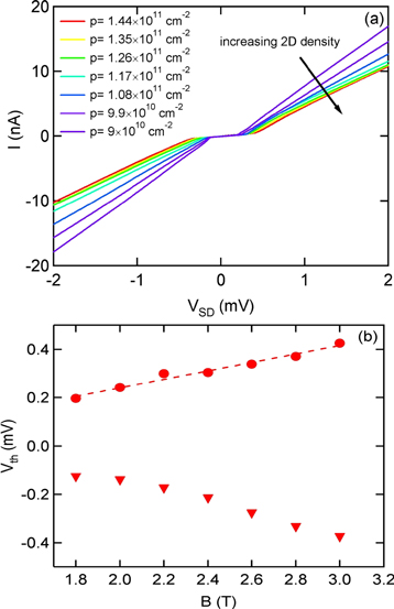
Figure 2. (a) IV traces for different VTG between −4 and −7 V in steps of 0.5 V corresponding to a density range  cm−2 and magnetic field range
  T. (b) Positive (circles) and negative (triangles) threshold voltages Vth extracted from figure 3(a) plotted vs B. The dashed line indicate the best linear fit through the data points (circles).
Download figure:
Standard image High-resolution imageHaving demonstrated the operation of the hole LL diode we use it to probe hyperfine coupling between hole and nuclear spins. The two characteristic signatures of hyperfine coupling observed in electron systems are: (1)hysteretic I–V traces and (2) time dependence of the source–drain current on the time scales of tens of seconds [7, 13, 14, 20, 21]. In electron Landau diodes, when a reverse bias is applied above the threshold voltage, electrons tunnel between spin polarized LLs with different spin orientations, so the electron spin has to flip. Some of the excess spin can be transferred to the nuclei via the hyperfine interaction. These electron–nuclear spin flip-flop processes build up a large net nuclear spin polarization over time. This polarization is detected as time dependent I–V characteristics via the effect of the nuclear Overhauser field on the electron Zeeman energy. For holes the situation is very different as the nature of the lowest two LLs is not simple spin  ; in general hole LLs are mixtures of heavy- and light-hole states [24]. Theoretical calculations for holes [24] suggest that the lowest LL is a pure HH state with total angular momentum
  . The second LL is mixed and has
  . In the LL diode, when the current flows between these two levels, the total angular momentum has to change by
  , which is a very inefficient process. This could lead to a suppressed nuclear spin polarization.
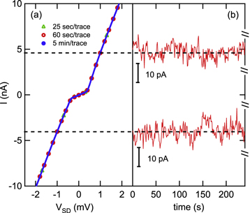
To look for hysteresis we sweep VSD back and forth. If the sweep rate is comparable to the nuclear polarization decay time (∼100 s), the I–V traces will show hysteresis [25]. Previous studies of electrically detected electron–nuclear spin coupling typically show  hysteresis due to nuclear spins [7, 15]. In contrast, in similar studies that used the LL technique [14] the magnitude of the hysteresis can exceed 100% allowing much more sensitive detection of nuclear spin polarization. Figure 3(a) shows three consecutive IV traces taken with a sweep time of 2560 and 300 s per trace. All traces sit on top of each other with no sign of hysteresis. To increase the sensitivity of our measurement, we look for time dependent current relaxation at several bias voltages above Vth for both positive and negative biases. First, we insure there is no nuclear spin polarization by setting the bias voltage to zero and waiting for 5 min. Then, we attempt to build up a nuclear spin polarization by rapidly (in
  ms) setting VSD to the selected operating point (from −5 mV to +5 mV in 0.5 mV intervals), to drive inter-LLs transitions. At the target VSD, we monitor the current as a function of time to detect any change in nuclear spin polarization through the Overhauser field. Similar measurements in electron LL diodes [25] revealed that the current exhibits an exponential time dependence with a time constant of 50 s independent of VSD. This time dependence is due to two competing processes [25]: nuclear spin polarization build-up (time constant ∼33 s) and nuclear polarization decay (time constant ∼100 s).
Figure 3. (a) Three IV traces measured with a different sweep rate ranging from 25 s per trace (greed open triangles), 60 s per trace (red open circles) and 5 min per trace (blue solid circles). (b) Two time traces taken at  mV for 4 min with a dwell of 5 min at
  V in between the time traces. The scale bars indicate the magnitude of current oscillations for a single trace with no averaging.
Download figure:
Standard image High-resolution image
Figure 3(b) shows two representative current traces measured in our device at  mV. We observe no sign of current relaxation down to the noise level in our experimental setup (20 pA). To reduce the noise even further we averaged over 20 traces to get down to 2 pA current noise and still there is no sign of current relaxation5
. In electron LL diodes [26], due to continuous pumping of electrons across the spin polarized edge states, large net nuclear spin polarization (
mV. We observe no sign of current relaxation down to the noise level in our experimental setup (20 pA). To reduce the noise even further we averaged over 20 traces to get down to 2 pA current noise and still there is no sign of current relaxation5
. In electron LL diodes [26], due to continuous pumping of electrons across the spin polarized edge states, large net nuclear spin polarization ( ) can be achieved and detected as a change in current through the device (∼1 nA). If we assume a similar nuclear spin polarization could be achieved in hole systems, the change in current would be an order of magnitude smaller (0.1 nA), due to the hyperfine coupling for holes is about ten times weaker than for electrons [8, 9]. Instead, in our measurements we cannot detect any current relaxation down to the noise floor in our measurement setup of 2 pA (for averaged measurements), indicating the maximum nuclear spin polarization polarization is less than 2% compared to that achieved with electrons.
Since both light and HHs are sensitive to nuclear spin polarization via the Overhauser field, the obstacle to detecting the hole–nuclear spin coupling is most likely the suppression of the spin flip-flop processes. Alternative methods of generating nuclear spin polarization include optical pumping [8] or the use of ambipolar devices [27] in which the nuclear spins can be polarized with electrons and detected with holes. Optical pumping is challenging, since the laser light will heat up the sample, which can mask small changes in current due to hole–nuclear spin coupling. We have attempted experiments with ambipolar devices, but found that the rapid reversing of the top gate voltage made the devices unsettled preventing detection of the small changes in current due to hole–nuclear spin coupling.
To summarize we have fabricated and characterized a LL spin diode in GaAs 2D hole system. We used the hole LL spin diode to show that surprisingly the splitting on the lowest two LLs is linear in B over the range of our measurements. We have observed no evidence of hyperfine coupling, indicating that hole–nuclear spin flip-flop processes are suppressed by at least a factor of 50 compared to GaAs electron systems.
Acknowledgments
This work was funded by the Australian Research Council through the Discovery Projects Program and by the Australian Government under the Australia–India Strategic Research Fund. We thank U Zülicke, R Winkler, IS Terekhov, EV Deviatov, VT Dolgopolov for illuminating discussions and E Marcellina and D Culcer for calculation of the Rashba and Dresselhaus energies. Experimental devices for this study were fabricated using the UNSW node of the ANNF.
Footnotes
- 4
Similarly to [14] the threshold voltage Vth is defined as the intersection of two lines fitted to the region where almost no current flows through the device and where large current flows through the device.
- 5
See supplementary materials available from stacks.iop.org/njp/17/033035/mmedia.