


Abstract
The (111)-2 × 1 surface of in situ cleaved heavily P- or B-doped Si is investigated by scanning tunnelling microscopy and spectroscopy at room temperature and at low temperature. P atoms have been identified on different sites of the Si(111)-2 × 1 surface by their characteristic voltage-dependent contrast for positive as well as negative buckling of the π-bonded chains. The distributions of dopants per surface area and of nearest-neighbour distances are found to be in agreement with a random arrangement of dopants in Si up to doping levels well above the metal–insulator transition. In addition, P atoms have been identified by their depth-dependent contrast down to the third layer beneath the surface with a volume density in agreement with the bulk doping density. The random electronic disorder supports the view of an Anderson transition driven by disorder close to the critical concentration or critical uniaxial stress.
Export citation and abstract BibTeX RIS

Content from this work may be used under the terms of the Creative Commons Attribution 3.0 licence. Any further distribution of this work must maintain attribution to the author(s) and the title of the work, journal citation and DOI.
1. Introduction
The transition between a metal with finite dc electrical conductivity σ(0) = σ(T → 0) and a non-metal with zero conductivity, known as the metal–insulator transition (MIT), has attracted considerable research interest starting with the seminal work of Mott [1]. Heavily doped semiconductors have been found to be excellent material to study the transition from localized to delocalized states with increasing doping level of donors or acceptors. Theoretically, the delocalization–localization MIT is driven by either disorder (Anderson transition) or electron–electron interactions (Mott–Hubbard transition), whereas in real systems both mechanisms must be considered. In this respect, heavily P- or B-doped silicon has been investigated in detail [2–4] to unravel the different contributions, to study the critical behaviour of the conductivity σ(N − Nc), where N is the charge carrier concentration and Nc the critical concentration, and to understand the role of the magnetic moments of the dopant atoms on the MIT.
A crucial point concerning the electronic transport of heavily doped Si and the physics of the MIT is the question of whether the dopants are distributed randomly or tend to form dimers or clusters at high doping levels close to Nc, where Nc = 3.52 × 1018 cm−3 for Si:P [4] and Nc = 4.06 × 1018 cm−3 for Si:B [3]. It is therefore mandatory to check for a random distribution of dopants in Si:P and Si:B. An elegant method is the preparation of clean surfaces by cleavage in ultra-high vacuum (UHV) and the identification of individual dopant atoms by scanning tunnelling microscopy (STM) and spectroscopy (STS) followed by a statistical analysis of their distribution at the surface.
STM on compound semiconductors has identified charged vacancies and dopants near the surface due to the charge-induced band bending of the local electronic density of states (DOS) [5–9]. The atomic structure and the local electronic properties of elemental semiconductors have been investigated by STM and STS since the early work of Stroscio et al [10] and Feenstra et al [11]. For doped Si, (111) and (100) surfaces have been studied. P dopants on the Si(001)-2 × 1 surface have been investigated after flashing the crystal to high temperature or by adsorption of PH3 and formation of a Si–P heterodimer [12, 13]. For Si(001), a c(4 × 2) reconstruction is observed at low temperatures which converts between 150 and 200 K to the strained 2 × 1 surface with deformations penetrating into the bulk [14]. The Si(111)-2 × 1 surface usually obtained by cleavage of a single crystal transforms into the stable Si(111)-7 × 7 reconstruction by heating above 600 K.
The physics of the single P donor in Si has recently attracted renewed interest due to the observation of photon echoes and Rabi oscillations and the possible coherent control of the Rydberg states of P donors in Si by THz radiation [15]. In a similar context, P atoms on the Si surface have been studied and manipulated by STM en route towards the fabrication of P qubits for a Si quantum computer [16].
In this paper we will focus on the 2 × 1 reconstructed (111) surface of heavily doped Si:P and Si:B which has been investigated by STM and STS with atomic resolution. We have identified substitutional dopants by their characteristic voltage-dependent contrast and have been able to attribute differences in the contrast patterns to different non-equivalent lattice sites of the P donor in the first and second atomic layers of the reconstructed surface. Signatures of P dopants have been found down to the third layer beneath the surface. The distribution of P and B dopants at the surface follows a distribution function derived from a Poisson distribution of randomly distributed dopants for doping levels above the MIT, thus showing that the P-derived electronic system presents a truly amorphous metal. We will discuss the issue of the MIT tuned by changing the doping level or applying uniaxial stress.
2. Experimental
Clean (111) surfaces of P- and B-doped Si were obtained by cleaving Czochralski grown single crystals6 at room temperature (RT) under UHV at a base pressure below 10−10 mbar. Samples with donor concentrations ND or acceptor concentrations NA in the range 1017–1020 cm−3 have been investigated. The cleaving procedure without further thermal treatment ensures that the distribution of dopants at the Si surface represents the original distribution in the bulk. The cleaved crystals were transferred in situ to a scanning tunnelling microscope. Experiments were performed in an Omicron STM-1 at RT and in a home-built low-temperature (LT) STM at T = 5–8 K. STM images (in constant current mode) and local dI/dV spectra were taken using clean tungsten tips with the tunnelling voltage applied to the sample. Hence, occupied (unoccupied) electronic states are imaged at negative (positive) tunnelling voltage V .
3. Si(111)-2 × 1 surface
The cleaved Si(111) surface exhibits a 2 × 1 reconstruction due to the formation of π-bonded chains oriented along the [ ] direction. Figure 1 shows a top view and a (
 ) cross section of Pandey's structure model which has been supported by several surface-sensitive investigations [17]. Along the [
 ] direction, Si atoms are located at positions 1 and 2 in the surface layer and at 3 and 4 in the second layer. The atoms of the π-bonded chain are threefold coordinated in contrast to the fourfold tetrahedral coordination in the bulk, leaving one dangling bond per chain atom. These dangling bonds form two surface bands with a band gap between them which provides the driving force for the different tilt or 'buckling' of the chains. Figure 1 represents the commonly used denotation of positive and negative buckling. For heavily doped Si, domains of opposite types of buckling and different energy gaps coexist at the surface at LTs as well as at RT [18, 19]. It has been argued that the relative abundances of the isomers depend on the size of the isomer domains and on the doping level due to a charge transfer between the domains [20]. For the two types of buckling, the relative positions of the surface bands in the band gap of bulk Si were determined by STS with high lateral resolution [19].

Figure 1. Top view and ( ) cut of the Si(111)-2 × 1 surface with (a) positively and (b) negatively buckled π-bonded chains extending along atom positions 1 and 2. Dashed lines indicate the 2 × 1 surface unit cell with lattice constants as = 0.384 nm and bs = 0.665 nm. The Si lattice constant is a = 0.543 nm.
Download figure:
Standard image High-resolution imageThe geometric arrangement of the atomic cores at the 2 × 1 surface has been obtained from ab initio calculations [21]. The height difference is 0.05 nm between the up-atom 1 and the down-atom 2 and 0.1 nm between the π-bonded chain and the second layer (atoms 3 and 4) [22]. Similar height differences have been obtained from an ab initio density functional theory (DFT) calculation for P/Si(111)-2 × 1 [23]. In that case, a P atom at site 1 protrudes more from the surface than a Si atom at this site. Similarly, a P atom at site 2 penetrates more into the surface than a Si atom would do at this site.
Local density approximation (LDA) calculations have shown that the π-bonded chain with negative buckling (figure 1, right) has the lowest total energy [24], which is slightly enhanced for positive buckling. However, at this point the LDA calculations seem to reach their limit.
First real-space observations of the Si(111)-2 × 1 surface and its local electronic structure were reported by Feenstra et al [11] and Stroscio et al [10]. In STM, only states at the elevated atoms 1 and 2 at the surface are imaged. STS experiments at RT and at LT provided further insight into the electronic structure of the surface unit cell for tunnelling voltages between −2 and +2 V [22, 25]. The details of the spectra were attributed to signatures arising from the surface valence and conduction bands within the volume band gap, in good agreement with ab initio calculations. The two variants of the π-bonded chain model (figure 1) differ only in the coupling of the surface to the volume and thus are difficult to distinguish by STM measurements.
For positive buckling, the surface band structure obtained from ab initio calculations [21] is in good agreement with photoemission and inverse photoemission data [26, 27]. Along the π-bonded chains the surface bands have considerable dispersion whereas in the perpendicular direction the bands are almost flat. This suggests that the surface can be considered as a one-dimensional system supporting earlier investigations by Northrup and Cohen [28]. Indeed, LT STS on Si(111)-2 × 1 indicates the formation of a Coulomb gap in the surface electronic DOS. The width of the Coulomb gap scales with the inverse length of the π-bonded chain segments which are generated by the truncation of π-bonded chains at terrace steps and/or at dopant atoms [29].
In addition, different types of antiphase boundaries exist at the Si(111)-2 × 1 surface [30, 37]. Their location can be manipulated by the STM tip, allowing a control of strain at the atomic scale [19, 37].
The different types of buckling affect the bandgaps at the surface and the depths of the space charge layer. Due to the heavy doping and the presence of surface states at the surface, the Fermi level EF is pinned just at the lower edge of the surface conduction band [19, 32]. The bandgap of the π-bonded chains has a width of 0.52 and 0.29 eV for positive and negative buckling, respectively. The difference is in qualitative agreement with the results from Busetti et al [18]. A similar reduction of the bandwidth was obtained from ab initio calculations [19]. The high density of surface states and the heavy doping of Si:P also give rise to a charge accumulation at the surface and a space charge that subsides into volume within a depth of 9–10 nm, slightly depending on the type of buckling [19]. For Si:B, similar estimates lead to a depletion layer with a depth of 3–4 nm [33]. In the bulk, the bandgap of Si is 1.1 eV at RT and 1.2 eV at LT.
4. Identifying individual dopant atoms at the Si(111)-2 × 1 surface
On the cleaved surface of heavily doped Si, a number of defects are generally observed. Apart from several adsorbate-induced features, one species exhibits a voltage-dependent contrast: an apparent protrusion at positive voltage and an apparent indentation at negative voltage for Si:P [25, 34] and vice versa for Si:B [33]. Features with such characteristic voltage-dependent contrasts have been observed on a number of P- or B-doped samples with various doping levels and are attributed to individual dopant atoms at the cleaved Si(111)-2 × 1 surface [25, 33, 34]. As an example figure 2 shows the STM image of a feature identified as a single P donor.
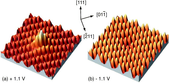
Figure 2. STM images (5 × 5 nm2) of the (111)-2 × 1 surface of P-doped Si (ND = 6.7 × 1018 cm−3) showing (a) a protrusion (apparent height 0.07 nm) at positive bias +1.1 V and (b) an indentation (apparent depth 0.03 nm) at negative bias −1.1 V at the site attributed to an individual P donor. RT, tunnelling current 0.3 nA [38].
Download figure:
Standard image High-resolution imageA similar change of contrast with variation of tunnelling voltage V and depending on the type of doping was observed for P and B dopants on H-terminated Si(111) [35]. The dopants were found to occupy sites in the second atomic layer due to the unfavourable additional bonding of a dopant to a H atom at the surface. A depth dependence was derived from the voltage-dependent 'visible' depth of the dopants in the STM image.
At RT the P donor is ionized giving rise to a local Coulomb potential at its site. This assumption was supported by an energy shift of ≈100 mV of the tunnelling spectrum at the P site compared to a spectrum taken at a defect-free area [25]. The local downward shift of the local DOS gives rise to an 'additional atom' observable for a tunnelling voltage corresponding to the surface band edge due to the occupation of an initially (in pure Si) unoccupied state by the local downward shift in energy. Such a local energy shift and an 'additional atom' were not observed at LT (T = 8 K) where the donor is not ionized and neutral. However, we have to note that the LT measurements were taken on surfaces of different samples with a different density of steps and defects which might influence the spectroscopic properties of the surface. This will be investigated in the future.
Figure 3 shows STM images of the (111)-2 × 1 surface of Si:P where a lateral shift of contrast perpendicular to the π-bonded chains is observed at reversed bias voltage. Detailed examination of a number of images shows that 50% of all investigated P-induced features show a shift of contrast of one row parallel to the [ ] direction, see figure 4. First images of P donors at the Si(111)-2 × 1 surface at RT already showed a shift of the contrast pattern perpendicular to the π-bonded chains [25]. The shift was attributed to P donors at position 3 or 4 that are imaged only due to an electronic coupling to the upper atom 1 or 2. This interpretation assumes that at RT all observed contrasts are caused by P donors in the upper two atomic layers. Additional effects have been reported for Sb and Bi dopants at the Si(111)-2 × 1 surface which have a much larger radius and therefore further reduce the total energy by pushing up the dopant atoms [36]. These effects are supposed to arise from dopants at different sites of the surface structure.

Figure 3. STM images (15 × 15 nm2) of the (111)-2 × 1 surface of Si:P (ND = 6 × 1019 cm−3) for (a) positive and (b) negative bias voltages [38]. RT, tunnelling current 0.3 nA. Arrows with black-filled tips indicate P donors with a voltage-dependent contrast which shifts one surface lattice constant bs = 0.67 nm along the [ ] direction by reversing the bias voltage. (c) Line scans along the blue or green arrow in the STM images. The dashed red line indicates a shift of the maximum at +1.2 V with respect to the minimum at −1.2 V of ≈1 nm. The blue curve is shifted upward by 50 units for clarity.
Download figure:
Standard image High-resolution image
Figure 4. 30 × 30 nm2 STM image of the (111)-2 × 1 surface of Si:P (ND = 6 × 1019 cm−3) at −1.2 V. RT, tunnelling current 0.3 nA [38]. White (black) circles indicate P donors that show no shift (a shift) in position when reversing the bias voltage.
Download figure:
Standard image High-resolution imageThe substitution of P atoms at non-equivalent sites has been studied in more detail at LT for P-doped Si [34]. For positively buckled π-bonded chains, four different contrast patterns induced by a P atom have been found. The assignment of the observed contrast patterns to the specific sites is based on geometric considerations in comparison with ab initio calculations. At the Si(111)-2 × 1 surface, the donor can be substituted at four inequivalent sites 1–4, see figure 1. Sites 1 and 2 are occupied by the up and down atoms of the π-bonded chain, respectively, 3 is a second-layer atom next to a down atom and 4 is a second-layer atom next to an up atom.
Figure 5 illustrates that the sites have different mirror symmetries. The mirror plane parallel to the [ ] direction (perpendicular to the chains) goes through the up atom for P at sites 1 and 4 (red arrow in figure 5) and through the down atom for P at sites 2 and 3 (green arrows in figure 5). For positive buckling, three contrast patterns could be attributed to a P atom located either at site 1, 3 or 4 [34], see figures 5(b)–(d). The fourth measured contrast pattern is not compatible with the calculations for position 2 and is presumably caused by a new reconstruction at the position of the P atom, see below. P atoms at site 1 show an extended contrast along one π-bonded chain with slightly reduced intensity at the two atoms in the centre for −0.5 V and an indentation in the same chain at an up-atom site for −1.0 V, see figure 5(b). The symmetry axis perpendicular to the chain of the elongated contrast crosses an up atom. For a P atom at site 2, the features should also appear in the same chain for both voltages but the mirror plane along the [
 ] direction should cross a down atom. However, such a contrast was not found [34]. For P atoms at site 3 or 4, the contrast enhancement at −0.5 V extends to two neighbouring chains (figure 5(c)). For P at site 3, the contrast is stronger in one chain than in the adjacent chain. The mirror axis crosses the down atom and at −1.0 V an indentation is visible in the chain which shows a weaker contrast compared to −0.5 V. P at site 4 leads to equally strong contrasts in the adjacent chains at −0.5 V and a strong indentation at an up-atom site in one of the chains at −1.0 V. The symmetry axis crosses an up atom (figure 5(d)).

Figure 5. STM voltage-dependent contrast patterns of P atoms at different binding sites in positively (a–e) and negatively (f–k) buckled π-bonded chains, tunnelling current 0.1 nA, T = 6 K. (a) and (f) Model of the surface unit cell illustrating the different symmetries of sites 1–4. (b) P atom at site 1, (g) P atom at site 2, (c) and (h) P atom at site 3, (d) and (i) P atom at site 4. (e) P atom in the positively buckled π-bonded chain at site 4 in pushed-up configuration. (k) P atom in the negatively buckled π-bonded chain at site 2 in pushed-up configuration reconstruction.
Download figure:
Standard image High-resolution imageFigure 5(e) shows an additional feature for which the mirror plane in the [ ] direction is at the up atom. Hence, the P atom must be located either at site 1 or 4. This P-induced contrast pattern is in remarkable agreement with STM images of Sb and Bi dopants located at site 4 [36]. Since Sb and Bi dopants at site 4 seem to form a new reconstruction where the donor atom is pushed out of the surface, this suggests that the P-induced signature in positively buckled
π-bonded chains in figure 5(e) is indeed a P atom at site 4 in a pushed-up reconstruction.
] direction is at the up atom. Hence, the P atom must be located either at site 1 or 4. This P-induced contrast pattern is in remarkable agreement with STM images of Sb and Bi dopants located at site 4 [36]. Since Sb and Bi dopants at site 4 seem to form a new reconstruction where the donor atom is pushed out of the surface, this suggests that the P-induced signature in positively buckled
π-bonded chains in figure 5(e) is indeed a P atom at site 4 in a pushed-up reconstruction.
The assignment of P donors to the four different sites has been investigated for negatively buckled π-bonded chains as well, see figures 5(f)–(k). These contrast patterns can be assigned to substitutional P atoms at sites 2–4. A characteristic feature fulfilling the geometric requirements of a P atom at site 1 was not found. Apart from the different voltages at which the contrast patterns occur, the signatures for P atoms at site 3 or 4 are identical for positive or negative buckling, see figures 5(c), (d), (h) and (i), respectively. The signature of a P atom at site 2 shows a distinct indentation for −0.5 V. Furthermore, the anisotropic contrast enhancement, visible also at −0.3 V, is strongly reduced at the P site and at the two neighbouring atoms (figure 5(g)).
A fourth signature observed for negatively buckled π-bonded chains is also a P atom at site 2 but with an altered configuration. At higher negative voltages, a protrusion located between two up atoms is visible. At −0.3 V, the same protrusion is still visible in addition to an anisotropic contrast. However, the maxima are increasingly shifted towards the up-atom sites with decreasing distance to the P atom (figure 5(k)). Again, comparison with STM data and DFT calculations for Bi and Sb at the Si(111)-2 × 1 surface [36] leads us to conclude that this altered signature might be caused by an upward buckling of the P atom. According to calculations, upward buckling of a P atom on site 2 is energetically slightly favourable with an energy gain of 40 meV [36, 37]. Hence, a feature characteristic of site 2 was only found in negatively but not in positively buckled domains while site 1 could only be observed in positively but not in negatively buckled areas.
Individual B acceptors at the Si(111)-2 × 1 surface have also been identified, see figure 6, with an apparent indentation at +1.2 V and an apparent protrusion at −1.2 V. It is reassuring that the sign change in the voltage-dependent contrast at ±1.2 V is correlated with the type of doping, i.e. n-type (Si:P) versus p-type (Si:B), although the detailed behaviour of the voltage-dependent contrast is different for P and B dopants.
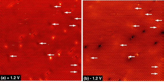
Figure 6. STM images (50 × 50 nm2) of the (111)-2 × 1 surface of Si:B (NA = 7 × 1018 cm−3) at (a) positive and (b) negative bias. RT, tunnelling current 0.7 nA. Arrows indicate features attributed to B acceptors at the surface.
Download figure:
Standard image High-resolution imageFor Si:B, a local upward band bending is expected at RT due to the negatively charged acceptor. However, an energy shift of the spectra as in Si:P could not be observed for Si:B because of a strongly modified DOS at the B acceptor. This is due to the different covalent bonding of the trivalent B atom to Si atoms compared to the bonding between P and Si atoms [33]. B at position 3 or 4 would have to participate in four bonds to Si. This would generate a charge transfer from Si to B which has been observed for B occupying subsurface positions [39, 40]. Moreover, the Si–B bond length is ≈12% shorter than the Si–Si bond length, leading to a considerable relaxation of the surface structure around a B atom. Unfortunately, further real-space investigations at LT on substitutional B atoms near the cleaved Si(111) surface have not been reported yet besides a first-principles calculation for B atoms beneath the H-terminated Si(111) surface [35].
5. Distribution of dopants at the Si(111)-2 × 1 surface
The voltage-dependent contrast allows a quantitative analysis of the distribution of dopants at the surface. For Si:P we have counted P-induced features on a number of images measured at RT within predetermined grids of area A. For ND = 6.7 × 1018 cm−3 we have chosen A = 900 nm2, for ND = 6 × 1019 cm−3 A = 94 nm2, thus keeping NDA constant. In the latter case, the analysis was done for a square grid as well as for rectangular grids with the long width aligned horizontally or vertically with respect to the image.
Figure 7(a) shows an example for the sample with ND = 6 × 1019 cm−3. The values obtained for the square grid differ only slightly from the average values obtained for the different rectangular grids. In both cases a broad distribution is observed indicating a random distribution of P atoms at the surface. A dopant superstructure or clustering of dopants would lead to a sharp maximum at a specific value of P atom/A. The solid line shows a Poisson distribution for a random arrangement of dopants at the surface, see the appendix, which is in reasonable agreement with the experimental values taking into account the small number of events.

Figure 7. (a) Distribution of observed P atoms per area A for a grid of squares (black bars) [38]. White bars indicate the average value evaluated from different rectangular grids. (b) and (c) Distribution of nearest-neighbour distances r for (b) P-doped Si [25] and (c) B-doped Si [33]. fA(r) and fV(r) are the functions derived from the Poisson distribution for dopants within a surface area A and in the volume V , respectively, see the appendix for details. fA(r) and fV(r) have been normalized to the total number of events.
Download figure:
Standard image High-resolution imageThe determination of a histogram of nearest-neighbour distances allows us to consider a larger number of data. For the analysis, we did not take into account dopants with a distance to the image border shorter than the distance to the nearest dopant atom. Figures 7(b) and (c) show the experimental data for the two most heavily doped Si:P and Si:B samples. Data have been collected with a bin width of 0.67 nm (distance of the [ ] rows). Again, each histogram shows a broad distribution in reasonable agreement with a distribution function fA(r) derived from a Poisson distribution, see the appendix. The broad distribution indicates that the dopant atoms are randomly distributed at the cleaved surface and hence in the volume for concentrations even above the MIT. For comparison we also plot the function fV(r) that would be observed if all P atoms distributed in the volume would contribute to the STM contrast at the surface. fV(r) strongly disagrees with the experimental data due to the fact that at RT only dopants located in the surface layer contribute to the STM image.
The average distances between P donors at the surface calculated for the considered dopant concentrations are  for Si:P and
  = 4.2 nm for Si:B, see the appendix, in good agreement with the experimental values
  and 4 nm, respectively, estimated from the experimental histogram. Note that these values are a factor of 2 smaller than for a regular distribution of dopants on a square grid, see the appendix. Missing data at large distances >6 nm are due to the fact that such values are rare because P atoms with large r values often have a shorter distance to the image border and have not been taken into account in our calculation.
The cut-off below ≈1.5 nm is significant, i.e. no r values below 1.3 nm (Si:P) or 1.67 nm (Si:B) are found. During crystallization and subsequent cooling in the Czochralski growth process, the dopants diffuse in the Si host and occupy lattice sites where dopant–dopant interactions—either electrostatic or mechanical due to inhomogeneous strains—are minimized. The solubility limits of randomly distributed substitutional dopants in Si are 1.2% (Si:B) [41] and 2.4% (Si:P) [42]. At the solubility limit, the energetically favourable configuration is the one where all dopant atoms are separated from each other as much as possible. As mentioned above, the average nearest-neighbour distance  is a factor of 2 smaller for a random distribution than for a regular distribution. Hence, considering a random distribution at the solubility limit should be a good estimate for the minimum nearest-neighbour distance which allows an energetically stable configuration. For Si:P the maximum distances at the solubility limit are
  in the volume and
  at the surface, where NSi = 5 × 1022 cm−3 is the density of Si atoms in the bulk and Ns = 1.6 × 1015 cm−2 is the density of Si atoms at the (111)-2 × 1 surface. For Si:B,
  and
and  are estimated from the solubility limits, respectively. These values are in good agreement with the low-distance cut-off observed for Si:P and Si:B which thus seem to be the characteristic minimum P–P or B–B distance governed by interactions between the dopants.
6. P atoms in subsurface layers
In STM, the 'visible depth' of dopants depends on both the dopant species and the tunnelling voltage. On H-terminated Si(111)-2 × 1, P and B dopants have been observed down to the third layer beneath the surface [43]. For cleaved Si(111)-2 × 1, large-scale multi-bias measurements (200 nm × 200 nm) with atomic resolution reveal signatures in addition to those found for P atoms in the surface layer (figure 8). These signatures show the same voltage dependence as the substitutional P atoms at the surface but they appear weaker with a larger lateral extension. The length of the anisotropic contrast enhancement in the π-bonded chain direction at −0.5 V is ≈10 nm for all features. At a voltage of +1.0 V, these signatures strongly resemble the contrast pattern of subsurface Sb atoms beneath the surface layer [36]. This suggests that the features might be interpreted as subsurface P atoms. For a check, the number of different features in the multi-bias images has been counted. The resolution of the images is just at the limit to resolve individual atoms and determine the site of the P donor exactly.

Figure 8. Topography images from a 200 nm × 200 nm multi-bias data set with atomic resolution at LT. Circles indicate P atoms in the surface layer (black), first subsurface layer (red), second subsurface layer (orange) and third subsurface layer (yellow). Tunnelling current 0.1 nA, T = 5.6 K. (a) STM image for V = + 1 V. (b)–(e) The white rectangle indicates the position of the zoomed-in areas displayed below.
Download figure:
Standard image High-resolution imageBy applying the criteria mentioned above for the assignment of the observed contrast patterns to specific P sites at the surface, we identified 11 P atoms at site 1, 34 P atoms at site 3, 33 P atoms at site 4, 56 pushed-up P atoms at site 4 and 76 adsorbate atoms. Twenty P atoms were found to be located in the surface layer without an assignment to a specific surface site. Altogether there are 154 P atoms in the surface layer in the investigated area of 200 nm × 200 nm (black circles in figure 8).
Concerning P atoms in subsurface layers, three slightly different contrast patterns depending on the depth can be distinguished. In the first layer beneath the surface, P atoms show only a small indentation at −2.0 V in contrast to the distinct indentation at surface sites and an elongated contrast at −0.5 V which is restricted to one of the three π-bonded chains. In some cases, an indentation above the P site is visible, similar to P atoms in the surface layer. At +1.0 V the protrusion is weaker and less localized compared to surface P atoms but still very distinct (red circles in figure 8).
The signature of P atoms in the second layer beneath the surface may only be surmised at −2.0 V while it is still visible at −0.5 and +1.0 V. In comparison with the first layer subsurface P atoms, the signatures are again fainter and less localized (orange circles in figure 8).
The feature attributed to P atoms located three layers beneath the surface appears as a weak spread-out protrusion at −0.5 and +1.0 V. At −0.5 V this protrusion is still elongated with a length of 10 nm along the π-bonded chains (yellow circles in figure 8). Summing up all features attributed to P atoms in the subsurface layer, we found 125 of the first, 140 of the second and 144 of the third type. Together with 154 P atoms in the surface layer, this gives a total number of 563 features distributed over four atomic layers with a total thickness of 1.24 nm and an area of 200 nm × 200 nm. This yields a dopant concentration of 563/(4.96 × 104 nm3) = 1.1 × 1019 cm−3 consistent with ND = 0.5 − 3 × 1019 cm−3 of the material according to the supplier. The almost constant number of each feature in each layer and the good agreement between the dopant concentrations in the as-prepared sample and the measured concentration confirms our assignment of P dopants in subsurface layers of Si. We note that the distribution of nearest-neighbour distances of P atoms in subsurface layers agrees well with a Poisson distribution which further supports a random arrangement of P dopants in the bulk.
7. Relation to electronic transport at the metal–insulator transition
The investigation of the MIT in doped semiconductors, especially silicon, has a long history. In particular, the role of the tuning parameters has been investigated in detail. Three different tuning parameters have been employed: carrier concentration N, uniaxial stress S and magnetic field B. The MIT can be driven by doping with donors [2] or acceptors [3], with measurements on different samples. Using a sample with a dopant level close to the critical concentration Nc, the MIT can be tuned by using uniaxial stress S. Here we discuss the critical properties close to the critical concentration Nc and critical stress Sc in the light of the main result of our STM work reported above, i.e. the random electronic disorder.
The physical mechanism of the change of the electrical conductivity lies in the fact that under uniaxial strain, the eigenfunctions of the originally cubic system no longer are eigenstates. Hence, the strain leads to an admixture of higher-energy eigenfunctions to the ground-state function. This may change drastically the spatial part of the wavefunction. A naive expectation suggests that for donor wavefunctions, the higher-energy ones are more extended; thus strain would lead to a stronger overlap with the result that strain drives an initially insulating system across the MIT. Conversely, for acceptor (hole) wavefunctions, the higher-energy wavefunctions are more strongly bound to the acceptor nucleus, and hence have smaller spatial extent with the result that an initially metallic acceptor system can be driven towards the insulating state. This different behaviour of donor and acceptor systems, e.g. Si:P and Si:B, is indeed generally observed [44–46]. In addition, the different covalent bonding and the concomitant change of the wavefunctions between P and Si versus B and Si might play a role. This is also inferred from the different local electronic properties of P and B at the Si(111)-2 × 1 surface, see section 4 and figure 6.
Recent detailed work on Si:P demonstrates a strong directional strain dependence of the conductivity σ measured at 4.2 K [47]. Strain along [110] leads to a monotonic increase of σ(S), strain along [100] shows a non-monotonic σ(S) dependence, while strain along [111] leads to a weak overall decrease of σ(S). These different behaviours all occur in the range of S up to 4 kbar. Still, the scaling behaviour of σ(S,T) is the same regardless of whether S∥ [110] or [100], as long as we restrict our data to the region where σ(S, 4.2 K) increases monotonically with S. In both cases similar critical exponents are obtained: z ≈ 3 for the dynamical exponent and y ≈ 1 for the correlation-length exponent [45, 47]. Even more, roughly the same exponents are found when applying σ(N,T) scaling for different samples close to Nc [48] although here the scatter between different samples is larger than that between different uniaxial strains for a given (single) sample. This is suggestive of a bona fide Anderson transition close to Nc or Sc driven by random disorder. In this respect, our STM observations corroborate this assignment. In particular, STM shows that interpretation of electronic-transport data in terms of clustering is not valid. Rather, a quantum-mechanical origin due to the overlap of wavefunctions is supported. In addition, STM provides proof for a minimal distance between P or B dopants. We note that away from criticality, the on-site Coulomb interaction becomes decisive and affects the electronic properties resulting in the splitting of the DOS into a lower and an upper Hubbard band [47]. In particular, features of a Mott–Hubbard transition come into play away from Nc. However, because of the random disorder, the Anderson transition sits in the 'driver's seat' and determines the critical behaviour.
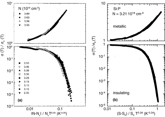
The scaling plots are shown in figures 9(a) and (b) for concentration-tuned [49] and stress-tuned [45] samples where we use the scaling function [45]:

Here t = N or S is the control parameter driving the MIT across the critical value tc, σc(T) = σ(tc,T) and y = 1/zν. The leading term of σc(T) is proportional to x = μ/νz where μ is the critical exponent of the conductivity, with x between 1 and 1.3 [45, 48, 50]. We note that the previous experiments [44] on the strain dependence of the conductivity of Si:P, with S∥ [ ], did not exhibit scaling [51].
Figure 9. (a) Dynamic scaling plot of σ(T)/σc versus  /NcTy with y = 0.33 [48]. Data were obtained in the LT range between 0.05 and 5 K. (b) Scaling plot of σ(T)/σc versus
  /ScTy with Sc = 1.75 kbar and y = 0.34 [45]. Data were obtained in the temperature range between 0.015 and 0.8 K for uniaxial stresses between 1 and 3.05 kbar applied along the crystallographic [100] direction.
Download figure:
Standard image High-resolution image
It is worth noting that while the scaling plot covers the same range of σ, i.e. 10−5 < σ/σc < 10, for both N and S tuning, the abscissa differs by a factor of ≈5. This difference signals the different microscopies of tuning: while the change of N retains the cubic symmetry when driving the MIT, this symmetry is lost upon application of uniaxial strain. This difference is also reflected in the different temperature dependences of σ(T) close to the MIT [45]. It is rewarding that these microscopic differences are not reflected in the scaling analysis of Si:P.
Turning finally to Si:B, we note that strong differences of the critical behaviour were found for N and S tuning [3, 46]. For instance, critical conductivity exponents were reported to be μ ≈ 0.7 for concentration [3] and 1.6 for strain tuning [46]. We speculate that these differences are due to the strong disturbance of the local environment around a boron impurity in Si discussed above.
8. Summary
STM and STS were used to investigate the local electronic properties of P and B dopants in Si for concentrations across the MIT. At the cleaved Si(111)-2 × 1 surface, individual P and B dopants were identified by their voltage-dependent contrast. A detailed analysis of the contrast patterns allows the assignment of P donors to the different substitutional sites at the Si(111)-2 × 1 surface. Signatures of weaker contrast with a larger lateral extension were attributed to P donors in subsurface layers. The statistical analysis of a number of STM images confirms a random distribution of dopants at the surface and in subsurface layers. Comparing P- and B-doped samples, the strong differences found in STS and in the critical behaviour of the electrical conductivity are possibly due to the different local environment of P and B atoms at substitutional sites in the Si host.
Acknowledgments
This work was supported by the Deutsche Forschungsgemeinschaft (DFG) through the DFG-Center for Functional Nanostructures and through project no. WE1889/3. We also acknowledge financial support from the Open Access Publishing Fund of the Karlsruhe Institute of Technology and the DFG.
Appendix
A.1. Distribution of nearest-neighbour distances
For Si with a dopant density ND, a density of Si atoms in the volume NSi = 5 × 1022 cm−3 and a density of Si atoms at the 2 × 1 surface Ns = 15.7 nm−2, the density of dopant atoms at the surface is ρ = NDNs/NSi = 3.14 × 10⁻⁸ cm ND.
The frequency of an event Ek to find k randomly distributed dopant atoms within an area A with a constant area density ρ is given by the Poisson distribution

The nearest-neighbour distance r is given by the product of the probability P(E0) that no dopant atom is found within a circular area A = πr2 and the probability P(E1) that exactly one dopant atom is found in a circular ring between r and Δr:

For small Δr ≪ r, the exponential term of P(E1) is ≈1 and the total probability is

with the distribution function

with  .
.
The average nearest-neighbour distance  of the distribution is

This is smaller than the average distance  of a regular arrangement of dopant atoms on a square grid.
The same calculation as before can be done for the volume, where the dopants are randomly distributed within a sphere of radius r with a constant volume density of dopants ND. One obtains a distribution function

and an average nearest-neighbour distance

Footnotes
- 6
Crystals were obtained from Wacker-Chemitronic GmbH, Burghausen.