
Abstract
The surface modification of superconducting radio frequency (SRF) cavities is mandatory to further push the limits in future accelerators. One strategy is the deposition of multilayer superconducting and insulating materials on top of the inner surface of an SRF cavity. Here, we report on a successful low-temperature coating of an SRF cavity with insulating  by thermal atomic layer deposition (ALD), without mitigating its maximum achievable accelerating field of more than 40 MV m−1. Furthermore, an improvement of the surface resistance above 30 MV m−1 has been observed, which is likely caused by an enhanced oxygen diffusion during the deposition process. Our results show that ALD is perfectly suited to provide a conformal coat to the interior of the cavity and to even modify and improve the properties of such devices.
Export citation and abstract BibTeX RIS

Original content from this work may be used under the terms of the Creative Commons Attribution 4.0 license. Any further distribution of this work must maintain attribution to the author(s) and the title of the work, journal citation and DOI.
1. Introduction
For more than two decades, superconducting radio frequency systems (SRF cavities) have continued to gain importance as one of the key technologies for modern accelerators. Research and development efforts carried out over many years have led to dedicated recipes for the optimum construction and treatment of SRF cavities made from pure niobium, yielding reliable performance and, for typical elliptical 1.3 GHz cavities, accelerating fields of up to 30 MV m−1, as successfully demonstrated in large scale accelerator facilities like the European XFEL or LCLS-II [1, 2]. New treatments have pushed even further, and individual cavities have achieved up to 45 MV m−1 [3–5, 8]. Yet, a hard limit is inevitable: the superheating field  of niobium, which translates to an accelerating field of 50 – 60 MV m−1 for this cavity geometry [6, 7].
In order to achieve groundbreaking improvements in SRF technology, new concepts for further enhancing accelerating fields and cavity performance have to be conceived, addressing the challenging demands posed by the planned upgrades of existing or the construction of future accelerators [9, 10]. Our approach targets one of the most promising research directions for advancement, the so-called superconductor–insulator–superconductor (SIS) or multilayer approach, in which the inner surface of Nb cavities is coated by alternating layers of a superconducting and an insulating material (see figure 1). This structuring was proposed by Gurevich in 2006 [11], and further theoretically developed to derive an optimal thickness of the layers needed to improve the RF performance [6, 12–15].
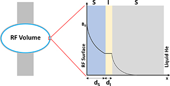
Figure 1. Left: schematic view of a superconducting cavity. Right: sketch of a multilayer SIS structure. A single superconducting layer with thickness  and a single insulating layer with thickness
  coating a superconducting substrate, in our case niobium. The y-axis shows the magnetic field and its decay in the SIS structure.
Download figure:
Standard image High-resolution imageCoating the inner surface of Nb cavities with thin films or multilayers of superconductors with higher critical temperatures than niobium, such as NbN or NbTiN, can produce composite accelerator cavities that are expected to outperform the best Nb cavities and achieve lower RF losses and higher accelerating gradients, potentially exceeding 100 MV m−1 [11]. This goal can be achieved by tailoring the deposited superconducting film, having a thickness of  with
with  being the London penetration depth of the coated superconductor and
  less than 100 nm. The higher critical magnetic field
  of these multilayers should exceed the superheating field
  of niobium, hence this would allow the application of higher accelerating fields compared to niobium. Thus, the thin higher-Hc
layers provide a magnetic screening of the bulk superconducting cavity preventing vortex penetration, which is further enhanced by the insulating layer with
of niobium, hence this would allow the application of higher accelerating fields compared to niobium. Thus, the thin higher-Hc
layers provide a magnetic screening of the bulk superconducting cavity preventing vortex penetration, which is further enhanced by the insulating layer with  . In addition, the surface resistance described by the Bardeen-Cooper-Schrieffer (BCS) theory of superconductivity is also strongly reduced because the targeted superconducting materials, e.g., NbTiN and NbN, have a larger superconducting gap Δ than Nb [16]. Hence, by employing such structures, the performance of superconducting cavities could be significantly increased compared to values typically obtained for pure niobium.
Experimental studies on samples, proving the field enhancement properties of SIS layers, and studies on deposition parameters correlating with material properties have been carried out [17–23]. While these studies were performed applying sputtering techniques to deposit the SIS films on flat samples, Proslier et al and Eremeev et al used thermal atomic layer deposition (ALD) to study the impact of an insulating  layer on cavities [24–27]. Similarly, Kato and Hayano coated samples within a 1.3 GHz single cell cavity with NbN by plasma enhanced-ALD, although no performance test was reported in this study [28]. Such studies on the deposition of insulating layers on an RF surface are required to understand the influence of the general coating process on the RF performance. Hence, it would be an important milestone on the way, to coat a cavity with a multilayer structure, to achieve a coating with an insulating layer without deteriorating the cavity performance.
Earlier studies of the thermal ALD coating of cavities by Proslier had additional layers of niobium pentoxide  on top of the
  layer, which was coated at
  or higher, and the cavities underwent various annealing steps between coatings. They observed a significant increase in field emission and multipacting, limiting several cavities to around 20 MV m−1 and an increased surface resistance [25]. Later studies with a new setup showed the same issue with a cavity, after coating it using the same parameters [26]. Although a cavity with an
  coating and a
  topping achieved accelerating fields of up to 33 MV m−1, this came with with increased surface resistance [27]. Motivated by these early findings, Eremeev et al tried to coat a cavity with
  using a temperature range of
  –
–  . After depositing, they observed a heavy discoloration in terms of a cloudy white color in some regions of the cavity surface. The cavity deteriorated significantly after the coating, and only after removing the coated layer was the RF performance recovered [24]. This cloudy white color can be interpreted as a consequence of a non-uniform coating, which was probably due to the temperature variation across the cavity surface in combination with unoptimized process parameters, e.g., purge times. Hence, a major aim of our work was to achieve a uniform coating, to maintain the RF performance after coating and prevent any field emission and multipacting.
Another question of interest is the actual impact of the insulating layer. The dielectric loss caused by such a layer in a SIS structure was estimated to be negligible, even for a layer thickness  of 100 nm [14]. On the other hand, studies implicate that the native dielectric
  layer contributes to the surface losses by various mechanisms [16, 29–32]. Therefore, it is not obvious if such an additional insulating layer indeed does not affect the RF performance, even more so without a superconducting layer on top, and if there might be a thickness threshold above which a negative impact becomes measurable.
2. Methods
As summarized in [33]: 'ALD is a chemical vapor deposition technique based on sequential input of two precursors separated in each case by an evacuation or purging step [34]. A sequence of exposure of the substrate to precursor A, evacuation (purging), exposure to precursor B, and evacuation (purging) constitutes a deposition cycle. In a typical ALD process the adsorption of each precursor is self-terminating after monolayer coverage.' In combination with the no-line-of-sight deposition, conformal coatings of three-dimensional large surface-area substrates with sub-nm thickness control — growth rates of 0.1 – 2 Å per cycle (GPC) — can be achieved [35–37]. As a consequence, the complex shape of our SRF cavity substrate is principally no obstacle to a homogeneous coating.
The deposition of  using trimethylaluminum (TMA)/water cycles is one of the most widely investigated ALD processes on different substrates such as metals, metal oxides and semiconductors, e.g. Si and GaAs [34, 38, 39]. In terms of the used TMA/water process, the reactive surface sites are −OH and −Al(
 ) for TMA and water, respectively.
  deposited by ALD is dense, stable and provides excellent dielectric passivization properties on metallic surfaces [40, 41]. High quality
  layers can be deposited using thermal ALD at a relatively low process temperature, below
  . These qualities make
  a promising material for use as an insulating layer that has been shown to preserve Nb superconductivity [42].
Our aims were, first, to reduce the deposition temperature compared to the  that Proslier et al used, and second, to achieve optimal properties without a subsequent annealing procedure. The motivation for the reduced coating temperature is based on the experience gained in past decades in the established annealing procedures of SRF cavities. Specifically, long resting duration of several hours, between 3 – 48 h, at temperatures between 120
  – 300
– 300  can already alter the performance significantly, due to the dissolution of the native oxide layers and various diffusion processes [43–48]. Hence, the impact of annealing taking place parasitically while coating has to be minimized.
The work was divided into three phases: first the recipe development was performed on samples, then the transfer of the optimized recipe to a test (dummy) cavity, and finally the coating of actual cavities. One should note that the cavity is not within a larger ALD chamber, but rather resembles the ALD chamber itself, and only the inner surface is coated.
All ALD processes of the  coatings were performed on an in-house developed thermal ALD system with a base pressure of
  , and using TMA and purified
  as precursors. After evacuating the cavity down to the base pressure, 20 SCCM of nitrogen 6.0 constantly flowed into the system as a carrier/purge gas, which led to an increase in the working base pressure to ≈
  . A typical pressure profile of two representative ALD cycles in our system is shown in figure 2(a).
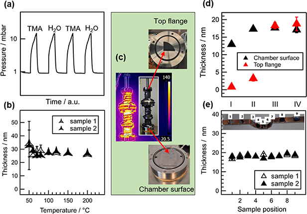
Figure 2. (a) Recorded pressure vs. time for two ALD cycles. One cycle proceeds as follows: a TMA pulse is followed by an exposure phase during which the TMA is chemisorbed by the exposed surface. After a purge with the help of nitrogen, an  pulse follows, also with exposure and purge phases. (b) Homogeneity of the thickness is compared for two samples for a temperature range of 50
  – 200
– 200  . Each data point is the average of 12 – 16 measurements across each sample and the errorbar is the rms value from table 1. (c) Left shows an infrared image taken of a dummy cavity with heating wires wound around it during a parameter scan. The inner surface area of a 1.3 GHz single-cell TESLA cavity that has to be coated is about
  . The height is 392 mm and the inner diameters of the cavity are 78 mm at the beam tubes and 206 mm at the cell [7]. The Si samples are placed at the bottom and top of the cavity. (d) Homogeneity of the film thicknesses compared for the top and bottom samples, placed as shown in (c) for the four different recipes described in table 2. (e) Thickness of the
  layer along the cavity surface for two coatings according to recipe III. Sample 9 is at the upmost position, while sample 1 at the lowest position in the cavity.
Download figure:
Standard image High-resolution imageTable 1. Durations for each process phase used for the temperature scans of 50  – 200
– 200  and a
and a  flow of 20 SCCM. The resulting thicknesses are shown in figure 2(b).
| TMA |

| Cycles | |||||
|---|---|---|---|---|---|---|---|
| Pulse (ms) | Exposure (s) | Purge (s) | Pulse (ms) | Exposure (s) | Purge (s) | ||
| 50 | 12 | 40 | 50 | 12 | 60 | 200 | |
Table 2. Recipes tested for  and a
and a  flow of 20 SCCM. Duration is given for each cycle phase figure 2(d).
| TMA |

| Cycles | |||||
|---|---|---|---|---|---|---|---|
| Pulse (ms) | Exposure (s) | Purge (s) | Pulse (ms) | Exposure (s) | Purge (s) | ||
| I | 50 | 12 | 120 | 50 | 12 | 120 | 100 |
| II | 250 | 45 | 120 | 500 | 45 | 120 | 100 |
| III | 500 | 60 | 120 | 500 | 60 | 120 | 100 |
| IV | 500 | 60 | 240 | 500 | 60 | 240 | 100 |
The recipe development was first performed on  /(100) Si wafer substrates and later also on conical shaped fine-grain Nb substrates. The deposition temperature ranged from 50
  –200
–200  , with target film thicknesses below 20 nm, being in agreement with the insulator thicknesses proposed for SIS structures. Further optimization was performed on a dummy cavity (see figure 2(c)) by placing reference Si substrates beneath the cavity and at the top flange while using heating wires to heat the cavity. In addition, a cavity-fitted sample holder with reference substrates placed inside the cavity was used. Note that to further improve the temperature control and homogeneity during the process, a tailor-made heating jacket fitting the cavity shape was used.
TMA was pulsed first into the cavity volume. The rotary vane vacuum pump was disconnected from the deposition chamber by a stop-valve during a defined exposure time, which allows for ligand-exchange and the completion of each of the half-cycle reactions. Each exposure was followed by purging, in which the pumping line was reconnected to the deposition chamber and all excess precursors and byproduct gases were removed. The TMA pulse was followed by an  pulse, which reacts with the surface and results in a hydroxylated monolayer of
  .
.
A detailed characterization study of samples was conducted using different standard analysis techniques. The thin film thickness on the samples was measured by spectroscopic ellipsometry (SENTECH, SENpro). The surface morphology and stoichiometry of different samples was analyzed by a high resolution SEM (Nova Nano SEM 450, FEI Thermofisher) equipped with an energy-dispersive x-ray (EDX) spectroscopy unit. The inner cavity surface was optically inspected by the OBACHT system [49]. The layered structure of the coated  film, the native niobium oxides and the bulk niobium was investigated by time-of flight secondary-ion mass spectroscopy (ION TOF SIMS IV).
The RF performance of the cavity was measured at the cryogenic test facility AMTF at DESY [50, 51]. The test obtains the quality factor Q0 as a function of the applied accelerating field  and the helium bath temperature. The uncertainties were calculated according to [52]. The quality factor is directly related to the surface resistance
  via
via  , with Γ as the so-called geometry factor. This geometry factor Γ only depends on the cavity shape and is a constant with the value of
  for the TESLA shaped single-cell cavity. The RF losses of a cavity, given by the surface resistance
  , is usually interpreted as the sum of two contributions:

with  as the contribution derived by the microscopic theory of superconductors [53] and
  is the residual resistance stemming from, e.g., scattering processes on lattice defects or interstitial atoms, dielectric losses in the native oxide and electric interface losses or trapped magnetic flux. Since trapped magnetic flux has a severe and important contribution [54–56], the magnetic environment of the cryostat is documented (and below
  ) and monitored during cooldowns [1].
3. Results
In this section, we present our results from the recipe development, leading to the successful coating of two superconducting niobium single-cell cavities with a thin  layer.
3.1. Recipe development
The aim of this part of our study was two-fold: (a) to identify a working set of parameters to achieve a homogeneous coating by an  layer for the large cavity surface, while (b) at the same time minimizing the associated annealing process by reducing the thermal budget, which is understood as the area under the temperature–time-curve, to reduce the impact of diffusion processes on the RF performance.
3.1.1. Sample studies.
The two important parameters for ALD processes are the processing times (pulsing, exposure and purging) and temperature. In our study, the first step was to identify the temperature range needed for the production of reproducible films. For this, we fixed the process times as shown in table 1, the  flow to 20 SCCM, and optimized the desired temperature in the range of 50
  –200
–200  . The films were grown on silicon wafer substrates with a size of
  . In order to check the reproducibility, two samples were placed and analyzed for each applied temperature.
The film thicknesses were obtained using spectroscopic ellipsometry by taking 12 – 16 measurements for each sample. Figure 2(b) shows the results of the temperature scan. A stable region was identified above  , matching the literature values [34, 57], and an operation temperature of
  was eventually chosen to allow for a certain margin in the temperature distribution on the surface.
The second step was the optimization of the process time for the individual pulse, exposure and purge steps. For this, we fixed the operational temperature to  , as it showed very reproducible films, a
  flow of 20 SCCM, and 100 process cycles. Note that, whereas the former study uses a standard ALD chamber for coating planar substrates, this study was conducted using a dummy cavity as chamber by itself and by placing Si substrates at the bottom and top of the cavity as shown in figure 2(c). These sample positions were selected to determine the recipe that leads to a full and homogeneous coverage of the cavity. For that reason, a series of recipes were tested, and table 2 summarizes the representatives shown herein, while figure 2(d) shows the film thicknesses of samples coated with those recipes described in table 2.
The recipe that had the same film thickness both at the bottom and top of the cavity within the shortest duration per cycle is recipe III.
The final step was to study the homogeneity of the film thickness within the dummy cavity. For that, a dedicated sample holder that matches the cavity shape was designed. Applying recipe III for 84 cycles to the dummy cavity in two different coating runs yielded a homogeneous coating of  along the cavity surface (see figure 2(e)), proving the excellent conformality and reproducibility of the ALD process. To summarize the result of the optimization, recipe III at
  was used to coat the niobium SRF cavities with a constant film thickness of 18 nm along the cavity.
A first study of the interface between the coated layer and the native niobium oxide and the niobium interface using secondary-ion mass spectrometry (SIMS) is shown in figure 3(a). Note that we used fine-grained Nb sheets, which are the same base material from which the Nb cavities are made.
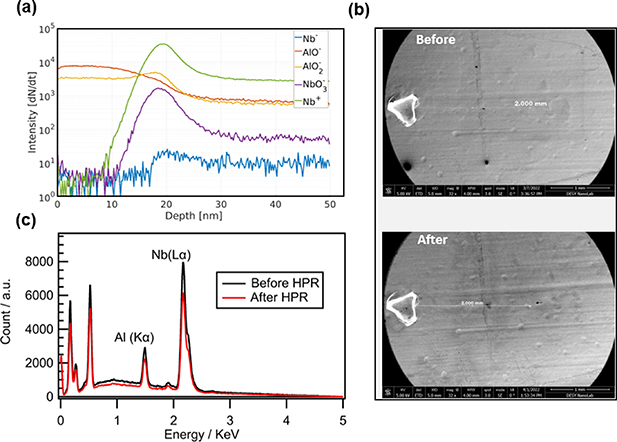
Figure 3. (a) Secondary ion concentration as a function of depth was obtained by SIMS measurement of a coated niobium sample. (b) Exemplary SEM images of the sample before (top) and after (bottom) undergoing seven HPR. The triangular shaped marker dent can be seen. No defects in the layer were found. (c) Energy-dispersive x-ray spectra taken before and after seven HPR. The Al peak is obvious.
Download figure:
Standard image High-resolution imageThe first  consisted of a pure aluminum oxide layer. An increase of the positive
  ion signal and various signals from
  ions with a change of the aluminum ion ratio between 10 – 25 nm show the convoluted interface. The
  signal rises above the noise level at 18 nm, and it indicated the start of the niobium oxide surface. The surface roughness of the sample tends to smear out potential sharp transitions, and a diffuse transition between 15 – 22 nm, with a change of the aluminum stoichiometry caused by the native niobium oxide, is obvious.
In order to obtain a 18 nm thick insulating  layer on a single-cell cavity, kept at
  , about 80 cycles are necessary, which resulted in a total time of 8h20' for the coating process. The deposition temperature is about two times lower compared to the ALD process applied by Proslier et al and the duration is six times shorter compared to the regular
  bake applied to SRF cavities. Hence, we achieved our goal to minimize the thermal budget.
3.1.2. Mechanical film stability.
To prevent particle contamination, causing electron field emission when an accelerating field is applied [58], cavities undergo a dedicated cleaning procedure in an ISO 4 cleanroom before testing [1, 59]. One step of this cleaning procedure is a high pressure rinse (HPR) with ultra pure (UP) water [60], which creates a mechanical pressure on the surface [59]. To confirm that the coated layer withstands this treatment and to check whether cracks or any damage appear, coated niobium samples were investigated with a scanning electron microscope (SEM) before and after multiple HPR. Results from Proslier et al. indicated that the layers should withstand the HPR. But since low-temperature ALD coated  films have a lower crack onset strain [61], it was necessary to test whether our films can withstand the HPR as well. The HPR of the samples was carried out in the same system, with the same parameters used for cavities, and with the same distance from the sample surface to the nozzle as for the cavity surface, to fully mimic the cavity cleaning procedure. In detail, one sample underwent one HPR, the second sample underwent seven HPRs. This procedure is equal to the cavity being ready for assembly (one HPR) or after assembly and ready for testing (seven HPRs). To help identify the same region, a dent was made on the sample surfaces as a marker before the coatings were made (see figure 3(b)).
The SEM inspection could not reveal any obvious defects (cracks, flakesor delamination) in the layer on both samples after the HPR, down to a resolution of 60 nm and EDX analysis confirmed the existence of the  layer on both samples before and after the HPRs (see figure 3(c)). Additional SIMS measurements on both samples further confirmed the existence of the
  layer with a thickness of around 18 nm after HPR. Hence, we have no doubts that a thin film coated on the inside of a cavity can withstand the regular test preparation.
3.2. Cavity coating
In this study, the coated cavities were 1.3 GHz single-cell TESLA cavities made out of high RRR niobium [7] and provided by DESY. Each cavity was cleaned inside the ISO4 cleanroom located at DESY, followed by the assembly of the required flanges for the ALD system. The cavity was then wrapped in cleanroom-foil and transported to the ALD system. The foil was opened, and the installation onto the system was done in a regular laboratory environment. Subsequently, a dedicated heating jacket around the cavity was installed. Local precautions to prevent particle contamination were taken. After coating the cavity using recipe III, the cavity was again wrapped in cleanroom-foil, brought back to the cleanroom, and there prepared for the cryogenic RF test. This preparation included a cleaning of the RF surface with an ultra-sonic rinse and an HPR with UP water where both preserve the coated layer as shown before.
3.2.1. Single-cell cavity 1Z1.
To prove that our developed recipe, cavity handling, and our deposition setup are capable of successfully coating an SRF cavity, we started with a cavity with a mediocre maximum accelerating field of ≈20 MV m−1.
The cavity was made of fine grain niobium with an RRR above 300. The treatment before the baseline measurement was an electro-polishing of  and a
and a  anneal. The cavity was limited by a quench, induced by an increased surface roughness [62–64], see the
The cavity underwent a baseline measurement, received a first 18 nm coating of  and was measured again to compare to the baseline. After that, it received another 18 nm coating, underwent the preparation procedure once more and was tested again. The comparison of the quality factor at 2 K for the baseline measurement to the first and second coating showed no significant difference (see figure 4). Although a trend may be seen, where a thicker coating results in a higher surface resistance, the observed average increase of
  for the second coating is still in the range of the measurement uncertainty. Note that no field emission was observed for both coatings.

Figure 4. Quality factor vs. accelerating field of 1Z1 measured at 2 K. The lines are only to guide the eye. The baseline (black) compared with the coating of the first 18 nm  (blue) and the second coating in total 36 nm (red).
Download figure:
Standard image High-resolution image3.2.2. Single-cell cavity 1DE18.
After confirming the process in the proof-of-principle test of 1Z1 that the recipe and setup worked, we coated a cavity that achieved a maximum accelerating field of 40 MV m−1 in the baseline measurement. With this, we intended to show that the coating maintains high accelerating fields without creating field emission. Furthermore, we wanted to study other possible additional loss mechanisms of the coating at higher fields.
The cavity was made of fine grain niobium with an RRR above 300 and underwent several treatments and tests before. The treatment before the baseline measurement was an electro-polishing of  and a
and a  anneal.
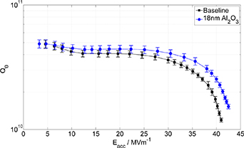
A comparison of the quality factor at 2 K for the baseline measurement before coating to the measurement after the 18 nm coating is shown in figure 5(a). The most important observation was the preservation of the extraordinary performance of the cavity. No deterioration whatsoever was observed due to the coating. To obtain the residual resistance  and the reduced gap
  , the surface resistance as a function of the temperature was measured, see figure 5(b). Note that the contribution from
  is suppressed at lower temperatures (i.e., 1.5 K) and the measured surface resistance is dominated by
  , as shown in figure 5(c). The residual resistance at
  remains unchanged: it was
  and
and  before and after the coating, respectively. In addition, the reduced gap was also unchanged: the values amount to
  and
and  before and after ALD coating, respectively. Noteworthy, and contrary to the fact that the residual resistance was unchanged within uncertainty at low accelerating fields, we observed a distinct difference at higher accelerating fields (>30 MV m−1). In detail, at low accelerating fields, the measurement almost equaled the regular
  vs. T measurement. But the surface resistance of the coated cavity decreased more slowly with increasing accelerating field than the cavity before coating. At 30 MV m−1, the surface resistance, i.e., residual resistance at this temperature, was improved by
  due to the coating. It is obvious that high accelerating fields can be maintained with a coating of
  .
.
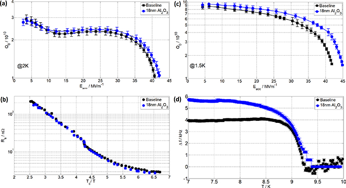
Figure 5. (a) Quality factor vs. accelerating field of 1DE18 measured at 2 K. The lines serve as a guide to the eye. The baseline (black) compared with the coating of 18 nm  (blue). (b) Surface resistance vs. inverse temperature for 1DE18 measured at
  . (c) Quality factor vs. accelerating field of 1DE18 measured at 1.5 K. (d) Frequency shift of the resonance frequency vs. temperature.
Download figure:
Standard image High-resolution imageTwo observations can be made from the measurement of the cavity frequency as a function of the temperature, shown in figure 5(d): first, an increase in the frequency shift compared to the baseline and, second, an unaltered  . Assuming the frequency shift solely comes from a change of the resonating volume, the shift can be converted into a change of the penetration depth
  of the RF field and an effective penetration depth λ0. This assumption is modeled by using Slater's Theorem and the Gorter–Casimir model [65, 66]. Calculating the effective penetration depth yields to
  for the coating, meaning the cavity is in the Pippard Limit and the resulting mean free path is in the range of typical values for cavity surfaces. In contrast, the effective penetration depth for the baseline only amounts to
  , which is unusually low. As this value shows an extremely clean surface, no mean free path can be derived.
4. Discussion
The recipe development was carried out in a systematic way on reference samples to map out the multidimensional parameter space, while keeping some boundary conditions, having the cavity surface in mind. To achieve a homogeneous coating of the cavity, process parameters, such as pulse and exposure time have to be taken into account, because the precursors take much longer to fill the large volume of the cavity and to cover the whole surface, compared to a small sample chamber. The optimized recipe also reduced the impact of the parasitic annealing, as it has a lower temperature compared to Proslier et al. [25]. Furthermore, the resulting  layer withstands the further cavity cleaning and preparation, which is a crucial prerequisite for a later implementation of the process into real cavity fabrication.
The first cavity, 1Z1, showed no significant change in the cavity performance after the first and even second coating of  , although a slight increase in the surface resistance was observed. This would be in agreement with models suggesting defective insulating materials contribute to RF surface losses, and hence by increasing the thickness, the contribution increases [16, 29–31]. Pushing further and also motivated by a report by Bira et al. [26], we then coated a cavity with a maximum accelerating field of 40 MV m−1. Bira et al. argued that their observed cavity limitation at 18 MV m−1 by multipacting arose from an inherent limitation of the
  layer. According to their reasoning, the surface is more prone to cascading tunneling effects since the secondary electron yield of
  is higher than that for niobium [67]. Their simulated emitted electron distribution peaks at 18 MV m−1 [26] as a build up of the emitted electrons. As no such effect was observed for 1Z1 up to 20 MV m−1, we wanted to enforce such an effect with higher applied fields. Hence, a high accelerating field cavity, namely 1DE18, underwent the baseline measurement, received an 18 nm coating of
  and was re-tested.
As 1DE18 was an excellent cavity before the coating, it was deemed as the perfect test to measure if the coating has any detrimental effect on the RF performance, especially with respect to field emission by multipacting. However, after the coating of 18 nm  no deterioration was observed. Our findings are in contrast to the observed multipacting by Bira et al, but it was also speculated that particle contamination prior to the coatings triggered the multipacting [25, 27]. Remarkably and by contrast, an increase of the quality factor above 30 MV m−1 is seen. Such an improvement could arise from two origins: (a) as Proslier already showed, the native niobium pentoxide
  layer is the origin of oxide defects, such as magnetic impurities, which can impact the residual surface resistance [30, 68]. As the
  might modify this niobium pentoxide
  during coating, the residual surface resistance might be improved this way. In the past, a similar effect of oxide-reduction by ALD-
 films grown on Sn-doped
  [69] or on
  /
/ films have been observed [70]. In both cases, the reduction of substrate surfaces, due to the very high reactivity of the TMA precursors, was observed by in-situ x-ray photoelectron spectroscopy (XPS) analysis after coating with ≈ 0.5 – 1 nm
  . Thus, during the first few cycles of the ALD process, TMA takes up oxygen mostly from the substrate surface and results in reduced substrate surfaces. (b) It is widely accepted that the improvement seen after the regular
  bake is caused by a modification of the mean free path within the RF surface [16] and a trapping of hydrogen at interstitial oxygen atoms, preventing the formation of lossy niobium hydrides at cryogenic temperatures [43, 44, 48, 71–73]. Hence, a similar process might occur here, and shows how important the tailoring of the thermal budget is for this process. An increase of the effective penetration depth compared to the baseline has been observed for both cavities after the coating, which goes along with a reduced mean free path, further supporting the oxygen diffusion hypothesis.
To shed light onto the mechanisms, a systematic sample study on the dynamics of the native niobium oxides during and after the coating is now underway. At the same time, it should be mentioned that  is not the only candidate for the insulator layer in an SIS structure. Aluminum nitride AlN has been known to stabilize and improve the superconducting properties of NbN or NbTiN films if it is used as buffer layer [74], and our own research has already shown that high
  are achievable on layered structures using AlN [75]. Hence, it is planned to investigate other insulating materials besides
  for future SIS studies, but also to continue the investigations of the potential beneficial effect of
  on the niobium oxides.
5. Conclusion
The RF results of two  -coated SRF cavities from our laboratory, including an
  -coated cavity achieving more than 40 MV m−1, are presented here. We showed that the coating does not have a detrimental effect on the accelerating field of the cavities, and even a reduction of the residual resistance above 25 MV m−1 is found. The origin of this improvement can be explained by either an oxide layer reconstruction or an enhanced oxygen diffusion into the lattice. The studies and results presented here are proof-of-principle experiments for further SIS studies and might pave the way to future experiments achieving an improved RF performance of cavities.
Acknowledgement
The authors M W and G K D have contributed equally to this paper. The authors acknowledge support from DESY (Hamburg, Germany), a member of the Helmholtz Association HGF. The authors thank R Monroy-Villa (DESY) for the frequency vs. temperature measurements and C Krill (Universität Ulm) for the usage of the thermal ALD system. The authors further thank T Proslier (CEA/Irfu) for discussions on the ALD coating of cavities. This work is supported by the BMBF under the research Grant 05K19GUB.
Data availability statement
The data generated and/or analysed during the current study are not publicly available for legal/ethical reasons but are available from the corresponding author on reasonable request.
Conflict of interest
The authors declare no competing interests.
: Appendix
Appendix. Single-cell cavity 1Z1
Subsequent optical inspections of the inner cavity surface after fabrication and each chemical surface treatment step showed the origin of the mediocre accelerating field to be a failed surface chemistry. This resulted in an increased surface roughness, pronouncing the grain topology and causing a superconducting breakdown, most likely due to local magnetic field enhancement (see figure 6). Also, the comparison of the quality factor for the baseline measurement at 1.8 K to the first coating showed no significant difference (see figure 7). The maximum difference in the surface resistance is an increase of  , which is below the measurement uncertainty of
  . For the second coating, this increase was measured to be
  and still within the measurement uncertainty. Yet, the same trend as for the 2 K measurement is seen, an increased resistance for the thicker
  layer, but still within the measurement uncertainty.
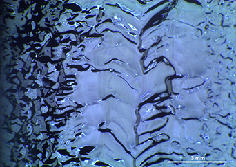
Figure 6. Image of the inner cavity surface of 1Z1 at the equatorial weld taken with the optical inspection system at DESY [49]. The pronounced grain boundaries, increasing the surface roughness, are obvious.
Download figure:
Standard image High-resolution image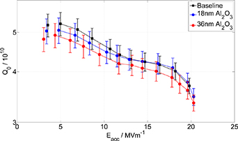
Figure 7. Quality factor vs. accelerating field for 1Z1 measured at 1.8 K. The lines are only to guide the eye. The baseline (black) compared with the coating of the first 18 nm  (blue) and the second coating (red).
Download figure:
Standard image High-resolution imageThe quality factor as a function of the temperature was measured and is shown in figure 8. The residual resistance remained unchanged at  for both measurements. The same is observed for the reduced gap: before the coating it was
  , while after the coating it was
  .
.
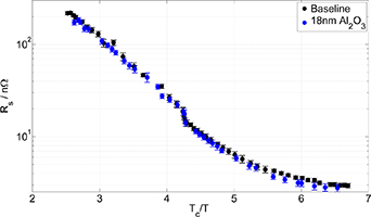
Figure 8. Surface resistance vs. inverse temperature for 1Z1 measured at  . The baseline (black) compared with the coating of the first 18 nm
  (blue).
Download figure:
Standard image High-resolution imageAppendix. Single-cell cavity 1DE18
The measurement at 1.8 K is shown in figure 9.
Figure 9. Quality factor vs. accelerating field for 1DE18 measured at 1.8 K. The lines are only to guide the eye. The baseline (black) compared with the coating of 18 nm  (blue).
Download figure:
Standard image High-resolution image