
Abstract
Interdigitated electrodes (IDEs) on dielectric films is an important electrode design in electrical components such as transducers and sensors. Further development and use of IDEs for characterization of the in-plane properties of dielectric films requires models for the capacitance, particularly when used in a multilayer stack. Previous models for the capacitance have permitted erroneous boundary conditions between layers with associated limitations to accuracy. In this work we present a new model based on fulfilling the boundary conditions between layers with different dielectric constant. We further demonstrate how the model can be used to calculate the in-plane dielectric constant and polarization of BaTiO3 films. The model is shown to outperform previous models using both the experimental data from BaTiO3 films on SrTiO3 substrates and finite element method simulations of the corresponding case. One important advantage compared to previous work is that the new model provides good results regardless of film thickness.
Export citation and abstract BibTeX RIS

Original content from this work may be used under the terms of the Creative Commons Attribution 4.0 license. Any further distribution of this work must maintain attribution to the author(s) and the title of the work, journal citation and DOI.
1. Introduction
Interdigitated electrodes (IDEs) are the most used electrodes for exploring the in-plane properties of dielectric thin films. Accurate characterization of dielectric properties of thin films with IDEs is highly relevant for applications such as tunable capacitors [1–3] and chemical sensors [4–9] that rely on change in material properties due to external stimuli. For devices that utilize the piezoelectric effect, such as surface acoustic wave devices [10–12] and piezoelectric transducers [13, 14], the dielectric properties must be understood in order to describe the electric field and coupling to the piezoelectric effect.
A model describing the electric field is required to couple material properties to the capacitance of IDE devices. The electric field surrounding infinitely spanning IDEs sandwiched between two infinitely spanning materials was solved analytically by Engan [15], while several approaches have been used to estimate the capacitance of IDEs in combination with a thin film. Ponamgi [16] addressed the boundary condition between different layers directly by generating additional potentials from the interface, and used this to generate a set of equations that could estimate the capacitance when solved by linear algebra. A similar approach of generating additional potentials, known as the method of recursive images, has recently been revisited by Diaz and Igreja [17], where unphysical boundary conditions at the interface with the electrode were used in order to preserve the potential at the electrodes. Wu et al [1] developed an alternate approach, known as the parallel partial capacitance (PPC) model, where the interfaces are instead ignored, and the structure is divided into partial structures and the capacitance of each partial structure is evaluated separately. Conformal mapping approaches of increasing accuracy were developed by Gevorgian et al [18] and Igreja and Dias [19]. However, improper treatment of boundary conditions still limits the accuracy of this approach [20, 21]. Moreover, other applications of IDEs may deviate from the basic design and include additional electrodes. This includes systems with electrodes both on top and below a thin film [22], or thin film with IDEs fabricated on a conducting substrate, where the substrate acts as a third electrode [13, 23]. The use of a conducting substrate was considered by Nguyen et al [24] as an additional contribution to the capacitance, but in general the inclusion of additional electrodes has not been addressed in the models previously described in literature.
Here, a numerical model for the capacitance of IDE structures in multilayer stacks is presented. The model is optimized to calculate the dielectric constant of a single layer on a substrate with known dielectric properties. Validation is provided by application of the model on experimental data for two BaTiO3 films on a SrTiO3 substrates combined with finite element method (FEM) simulations. BaTiO3 was chosen as it is a prototype ferroelectric material with well-known properties. Finally, a Python implementation of the model is available on Github [25], including examples of use for a variety of geometries.
2. The model
2.1. Layout of IDEs
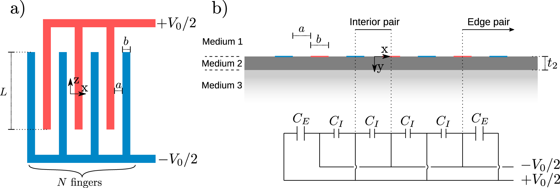
The layout of a set of IDEs in the x-z plane is shown in figure 1(a). The IDEs consist of two comb electrodes with a total of N fingers. The fingers with positive potential overlaps with the fingers with negative potential in a region of length L in the z direction. Here we assume that the ratio between the periodicity of the electrodes and L is such that fringe effects at the end of the fingers are negligible and can be ignored. A cross section of the structure (x-y plane) is shown in figure 1(b). The spacing between the electrodes, a, and the finger width, b, are indicated. The figure shows a general design with one layer of finite thickness (medium 2, with thickness t2), between two layers of infinite thickness (medium 1 and medium 3).

Figure 1. (a) Geometry of a set of interdigitated electrodes in the x-z plane. The finger overlap length L and number of fingers N are indicated. (b) A cross section of (a), showing the x-y plane. The electrode width b, electrode spacing a, and thickness of medium 2 (t2), are indicated. An equivalent circuit model of the cross section is also shown. Each interior pair of electrodes is assumed to have capacitance per unit length CI , while the edge pairs have a capacitance per unit length CE .
Download figure:
Standard image High-resolution imageFor this work we describe the geometry by the cover fraction  [19] and the normalized thickness of medium 2,
  . Normalizing the geometry also gives rise to the dimensionless coordinates
  and
and  .
.
The total capacitance of the structure can be estimated by considering the individual capacitance between each pair of fingers. Following the route of reference [19], we only consider edge effects at the outermost electrode pairs (capacitance per unit length CE ), while periodic boundary conditions are used when considering the interior electrodes (capacitance per unit length CI ). An equivalent circuit diagram is shown in figure 1(b), and the total capacitance of the structure can be estimated as follows:

2.2. The capacitance of interior fingers
The potential in the case where the thickness of medium 2 reaches infinity (i.e.
 ) may be calculated as described by Engan [15], Wu et al [1], Wei [12], or Igreja and Dias [19]. We will use the subscript
  to mark the capacitance per unit length,
  , and potential,
  , for this case. The required expressions for calculating
  and
and  using both a conformal mapping approach [19] and a Fourier approach [15] are included in section 1 of the Supporting Information (stacks.iop.org/SMS/29/115039/mmedia).
Given a finite thickness of medium 2, as shown in figure 1(b), boundary conditions at the interface between medium 2 and medium 3 must be fulfilled. The same is true for the interface between medium 2 and 1 between the electrode fingers. Using the initial field  as a basis, we here use the method of recursive images to fulfil the boundary conditions between the layers [17]. This will distort the constant potential at the electrodes, and we will address this distortion later. In the method of recursive images, a forward and a reverse potential is generated whenever a potential interacts with the boundary conditions at an interface. These potentials are defined using the forward,
  , and reverse,
  , coefficients for the respective interface defined by the dielectric constant ε(i) and ε(j) in medium i and j [16, 17]. A derivation of the coefficients from the boundary conditions is included in section 2 of the Supporting Information, where anisotropic materials are also considered. The three first generations of potentials in the method of recursive images are illustrated in figure 2(a)–(c). Equation (2) describes the sum of all partial potentials generated, VI1(x, y), and this potential is illustrated in figure 2(d), while figure 2(e) shows the potential along the interface with the electrodes.

Figure 2. Method of recursive images. (a) The initial potential  is projected into medium 1 and 2. (b) The first reverse and forward potentials. (c) The reverse potential in (b) generates the set of reverse and forward potentials shown in (c). (d) The sum of the infinite series of reverse and forward potentials generated. (e) The total potential at the interface between material 1 and 2.
Download figure:
Standard image High-resolution image

The potential, VI1(x, y), and the associated capacitance, CI1, are denoted with the subscript 1, as we will soon place them in the context of a series of similar potentials. It can be seen from figure 2(d) and (e) that the potential VI1(x, y) does not respect boundary conditions (± 0.5 V) at the electrodes. The total displacement field in the x direction remains constant when using the method of recursive images, so that CI1 can be calculated using the expression for  .
.
We now proceed to use linear algebra to address the non-constant potential at the electrodes. For this approach we generate a series of potentials VIi with ever decreasing cover fraction ηi with i = 1...M. Any linear combination of these potentials, will fulfil the boundary conditions at all interfaces with the exception of the electrodes, and we seek a linear combination that will approximate correct boundary conditions also here. The combined potential VIc (x, y) and capacitance CIc may be found if appropriate weights ui are known:


The weights ui may be found by using linear algebra to balance the potential at M locations along the electrode surface, denoted xj with j = 1...M. A linear distribution of cover fractions ηi and locations xj is chosen for simplicity, as detailed by equations (5) and 6:


Solving the linear algebra problem in equation (7) will then yield the weights ui . Here V0 is the potential applied to the electrodes, and is set to 1 V.

An example of the potential described by a linear combination of M = 4 components is shown in figure 3(a) and (b), while each of the 4 components are shown separately in figures 3(c)–(f). It can be clearly seen that VIc (x, y) is in reasonable agreement with the boundary conditions that require +0.5 V at the left electrode and −0.5 V at the right electrode.

Figure 3. Example of potential using the proposed model with 4 components. (a) The combined potential using four components. (b) the potential along the interface with the electrodes. (c)–(f) The potential of the four components used for the combined potential in (a).
Download figure:
Standard image High-resolution image2.3. The in-plane polarization in a ferroelectric thin film
We here propose a method for estimating the average in-plane polarization in the film at the plane midway between the electrode fingers (x = 0). At this plane, the displacement field is parallel to the x-axis, and distributed between the film, substrate, and air. By estimating the sum of the displacement fields in the substrate and air using the proposed model, these can be subtracted from the charge collected by the electrodes in order to calculate the polarization in the film as given in equation (8). Here  is the experimentally collected charge at the electrodes, and
  and
and  are the integrated displacement fields in substrate and air, respectively.
  and
and  can be calculated based on the potential given by equation (3) by approximating the film as a homogeneous non-ferroelectric material. The details for calculating
  and
and  are provided in section 3 of the Supporting Information. The polarization, P, is may then be calculated according to equation (8):

2.4. Capacitance of the edge pair
The capacitance of an exterior pair of electrodes was approximated by Igreja and Dias [19] by assuming a plane of constant potential at the center of the outermost electrode gap, and with no flux passing the plane at the center of the next-to-outermost electrode. Using these approximations, the edge capacitance can be calculated as follows:

where the subscript 2 denotes a set of IDEs with only two electrode fingers. Equations (2), 7 and 4 may easily be adapted to calculate C2c
using the initial potential  , as detailed in section 4 of the Supporting Information.
2.5. Multiple sets of electrodes
The linear algebra approach in equation (7) may be expanded to include additional electrodes at different interfaces in a multilayer stack, and the implementation of this model available on Github is to handle any number of layers with an arbitrary number of electrodes [25]. This may for example be interdigitated electrodes on top of one or more thin films grown on a conducting substrate, where the substrate acts as a separate electrode [13, 23], or alternatively systems with electrodes on both sides of a film [22]. The potential of such systems are illustrated in section 5 of the Supporting Information.
2.6. Anisotropic materials


3. Experimental
Two (100) oriented BaTiO3 films 47.4± 1.1 nm and 142.2± 1.0 nm thick deposited on (100) SrTiO3 substrates (10× 10× 0.5 mm, Crystal GmbH, Berlin, Germany) were fabricated to obtain experimental data for the validation of the model. The films were prepared by a chemical solution deposition prosess reported elsewhere [26]. The (100) BaTiO3 films are under tensile strain due to the mismatch in thermal expansion between SrTiO3 and BaTiO3 [26], and this is suggested to give an  domain pattern, which has recently been confirmed [27]. The mismatch between the lattice parameter of the substrate and film is relaxed by lattice dislocations at the interface [28]. The thickness of each film was measured by transmission electron microscopy, with images included in section 6 of the Supporting Information.
The electrodes were deposited using lift-off and e-beam evaportaion of 5 nm Ti and 20 nm Pt [26]. Six sets of IDEs, each with a 1× 1 mm footprint, were patterned on each of the two films, with the fingers aligned along the [010] pseudo-cubic axis of the film. The finger spacings (a) varied from 3 to 15 µm and the finger width (b) varied in the range 1.5 to 3.2 µm. The electrode widths and gaps were measured using an automated image analysis procedure and the uncertainty in the widths was ± 80 nm. The geometries of the IDEs are tabulated in section 7 of the Supporting Information.
Electrical characterization at 1 kHz was performed using an Aixacct TF2000 thin film analyser with a ceramic thin-film sample holder (aixACCT Systems GmbH, Aachen, Germany). The small signal voltage was varied so that the corresponding characteristic in-plane electric field,  , in the film between the electrode fingers was 0.2 kV cm−1, calculated by as follows [24]:

where V is the applied voltage. A bias sweep was performed with a frequency of 0.1 Hz and an amplitude of 20 kV cm−1. The dielectric constant of the SrTiO3 substrate was determined to be 317± 1.2, based on measurements from IDEs on a pure SrTiO3 substrate (not shown). The dielectric constant of the substrate was found to be independent of the applied voltage in the range relevant for this study. Charge-potential hysteresis loops were captured at 30 Hz.
M = 16 components were used for the model when determining the dielectric constant of the film from the experimental capacitance. Both the film and substrate were treated as isotropic in the verification of the model.
3.1. Finite element method (FEM) simulations
The FEM simulations were performed using the FEMM software [29]. For calculating the interior capacitance, CI,FEM , a cell was made with dimensions (a + b)× 4(a + b) and with Neumann boundary conditions (zero flux) on all outside boundaries. For the vertical boundaries this is equivalent to a periodic boundary condition. The limited height of the cell reduces the accuracy, but with the height used here the reduction in accuracy was not found to be significant. The grid density was varied depending on τ2, as thinner films require higher grid density to obtain sufficient accuracy. Up to 1 million nodes were used for the simulations. By assuming that the capacitance calculated by FEM is accurate, we can evaluate the accuracy of the model presented here as follows:

4. Results
4.1. Application of the model to BaTiO3 films on SrTiO3 substrates
The capacitances measured using geometrically different IDEs on the two films are shown in figure 4(a) and (b), where the capacitance has been normalized with respect to the number of gaps and the finger length. Based on the capacitance data, the dielectric constant was calculated using the model and the resulting dielectric constant-electric field, ε(2)–E, loops are shown in figure 4(c) and (d). The relative dielectric constant in the BaTiO3 films at zero field is 1911± 118, and 3013 ± 148 for the thick and thin film, respectively. The dielectric constant as calculated using the PPC model is shown for comparison. The constituent equations of the PPC model are included in section 8 of the Supporting Information [19].

Figure 4. The capacitance of the BaTiO3 films with thickness (t2) of 142 nm (a) and 47 nm (b). The capacitance is normalized with respect to the finger length L and number of fingers gaps (N − 1). The calculated dielectric constant, ε2, as function of applied bias of the BaTiO3 films with thickness 142 nm (c) and 47 nm (d). The value at zero field is indicated for both films.
Download figure:
Standard image High-resolution imageA sensitivity analysis of the calculated dielectric constant with respect to the geometric parameters is included in section 9 of the Supporting information. Given the uncertainty of the geometric parameters, an uncertainty of ∼ 100 is expected for the dielectric constant of the thick film. The sensitivity analysis also examined the impact of anisotropy in the dielectric constant of the film, and it was found that the capacitance has much higher sensitivity to the in-plane component than the out-of-plane component.
Capacitance curves generated by the model using the field-dependent permittivity of figures 4(c) and (d) are presented in section 10 of the Supporting Information. The calculated capacitance curves represent a good fit to the experimental curves.
The charge collected at the electrodes when performing a voltage sweep is shown in figure 5(a) and (b) for the thick and thin films, respectively. A large capacitive contribution from the substrate can be seen in the slope of the curves. Figure 5(c) and (d) shows the polarization in the BaTiO3 films as calculated by equation (8), where the contributions from the substrate and air have been subtracted using the model. The remnant polarization was found to be 10.54± 0.87 µC cm−2 and 5.75± 0.67 µC cm−2 for the thick and thin films, respectively, while the coercive field was 5.88± 0.14 kV cm−1 and 5.48± 0.21 kV cm−1.

Figure 5. The collected charge at the electrodes of the BaTiO3 films with thicknesses, t2, of 142 nm (a) and 47 nm (b). The charge is normalized with respect to the film thickness t2, finger length L and number of fingers gaps (N − 1). The polarization calculated using equation (8) of the BaTiO3 films with thickness 142 nm (c) and 47 nm (d).
Download figure:
Standard image High-resolution image4.2. Evaluation of the model by FEM
The accuracy of the model compared to FEM (equation (11)) for a structure with an infinite number of fingers (CIc ) is shown in figures 6(a)–(c) using a varying number of components M. The accuracy of the PPC model is shown in figure 6(d) for comparison. The accuracy of the proposed model is maximum when considering a thick film with a low cover fraction. When a single component is used, the accuracy is higher or comparable to that of the PPC model for the entire region probed. The accuracy increases with increasing number of components. When using M = 4 components, the model has more than 99 % accuracy for the geometries used to obtain the experimental data in figures 4 and 5. The PPC model has an accuracy greater than 92 % for the same geometries, a difference of 7 percentage points. The relative uncertainty of the FEM simulations used to compare the models is estimated to be 0.1 % based on the finite grid density and simulated cell height.

Figure 6. The accuracy (equation (11)) of the model when compared to FEM as a function of τ2 and η for M = 1 (a), M = 2 (b) and M = 4 (c). The stars in (c) and (d) mark the geometries used for the experimental data presented in figure 4, while the circle in (c) marks the geometry shown in figure 3. (d) Accuracy of the PPC model when compared to FEM.
Download figure:
Standard image High-resolution image
5. Discussion
IDEs with different geometrical dimensions deposited the two BaTiO3 films formed the basis for experimental verification of the model. The hysteresis loops for the different IDE geometries, shown in figure 4 and 5, are superimposed on each other. The data shown in figures 4(c) and (d) clearly demonstrate that the model gives a consistent field-dependent capacitance for both the thick and thin films. Moreover, the polarization-electric field hysteresis loops, shown in figures 5(c) and (d), show that we can also calculate the polarization versus electric field. However, equation (7) used to calculate polarization are based on several approximations, and a more accurate equation for the polarization can be further developed. Finally, the two films do not have the same electrical properties, which we will return to in the end of this section.
The dielectric constant of BaTiO3 is anisotropic [30], and crystallographically textured BaTiO3 films are therefore anisotropic in nature [31], but the sensitivity analysis (section 9, Supporting Information) demonstrates that the out-of-plane component of the dielectric constant of the two BaTiO3 films has only a minor effect on the measured capacitance of the system investigated here. The error due to neglection of the anisotropic contribution is therefore low. The low sensitivity to the out-of-plane component is related to the high ratio between the electrode spacing and film thickness used for this study (low τ2), which results in a homogenous in-plane electric field in the BaTiO3 films between the electrode fingers. Furthermore, the low sensitivity to the out-of-plane component implies that the (isotropic) dielectric constant found here can be treated as an approximation of the in-plane component of the dielectric constant in the film.
The model developed here outperforms the PPC model as evident by the lower distribution in the calculated dielectric constant (figures 4(c) and (d)). A similar trend is observed when the two models are compared to results from FEM, where the model outperforms the PPC model for both periodic structures (figure 6), and when considering structures with a limited number of fingers (section 11 of the Supporting Information). For an anisotropic film, a validation by FEM is included together with the constituent equations in section 2 of the Supporting Information.
The electrodes were oriented along the [010] direction so that the electric field was applied primarily along the [100] in-plane direction of the BaTiO3 films. The films have an  in-plane domain pattern, with the polar axis alternating between the [010] and [100] in-plane directions [26]. The observed dielectric constants of the films are within the range observed for BaTiO3 single crystals with 4000 along the polar axis and 200 orthogonal to the polar axis [30], while the remnant polarization is lower than that of single crystals (26 µC cm−1) [32]. The intermediate dielectric constant and lower polarization when compared to single crystal BaTiO3 is expected, considering the proposed
  domain pattern. The remnant polarization is comparable to what has recently been achieved in-plane for a 80 nm BaTiO3 films grown by pulsed laser deposition on NdScO3 (12 µC cm−1) [33]. The dielectric constant and remnant polarization are calculated by assuming a homogeneous film. However, the epitaxial coupling with the substrate will yield compressive strain at the interface [34], while away from this interface the film is relaxed by edge dislocations and will experience tensile strain due to a difference in the thermal expansion coefficient [26]. The in-plane properties depend on the strain state, where compressive strain favours a high in-plane dielectric constant, and tensile strain favours high in-plane polarization [31]. The film properties obtained by assuming a homogeneous film are therefore expected to be thickness dependent. For the two films examined here, a lower average polarization and a higher dielectric constant are found for the thinner film, consistent with the suggested inhomogeneity.
The effect of piezoelectricity has not been considered for this work. The piezoelectric effect impacts the anisotropy in the dielectric constant, as the films are clamped in the in-plane directions, but free to move in the out-of-plane direction. Thus, the dielectric constant is expected to correspond to the effective permittivity for a film with interdigitated electrodes. Equations of state for such films were discussed in [35].
6. Conclusion
A new model for the capacitance and potential of IDEs was presented and it was shown that the new model was more accurate than the PPC model both when applied to experimental data, and when compared to FEM. The model is applicable for more geometries, such as systems where a conducting substrate is used as a support for a multilayer stack with IDEs, or where one or more layers have an anisotropic dielectric constant. Furthermore, a method for calculating the in-plane polarization of a ferroelectric film has been demonstrated using the proposed model. A full implementation of the model is available on Github, including examples for a variety of geometries.
Acknowledgments
The Research Council of Norway is acknowledged for support to the Norwegian Micro- and Nano-Fabrication Facility, NorFab, project number 245963/F50 and the Advanced Piezoelectric Devices project, project number 273248. Special thanks to Inger-Emma Nylund, NTNU, for preparing TEM lamella of the films and imaging the cross section in TEM.