

Abstract
This paper investigates the field-effect sidewall surface passivation of III-Nitride blue light emitting diodes (LEDs) using ultrathin films of Al2O3 and ZnO grown using atomic layer deposition. A large density of negative fixed charges existing at the sidewall surface of the passivation layer leads to formation of an electric field at the interface of the passivation layer and the GaN layer. This repels the free negative charge carriers from getting close to the surface of the semiconductor and being trapped there. It also reduces the non-radiative recombination of these charge carriers and eventually leads to enhancement in electrical and optical properties of these devices. Electrical measurements demonstrate a significant decrease in the leakage current and the ideality factor in addition to a notable increase in the parasitic shunt resistance of the field-effect-passivated GaN LEDs compared to non-passivated devices. The field-effect passivation can be especially useful for smaller LED die size. In such a device, the effect of high leakage current at the edges of the device is more detrimental to its performance. The proposed approach can further eliminate the shunt conduction paths along the sidewalls of the LED and increase the efficiency of the devices.
Export citation and abstract BibTeX RIS
1. Introduction
III-Nitride (III-N) semiconductor materials have attracted much attention for their wide application in high efficiency optoelectronic devices, including light emitting diodes (LEDs), photodiodes, laser diodes, and solar cells [1, 2]. However, a relatively large leakage current in these devices can severely reduce their reliability, lifetime, electrostatic discharge resilience, and subsequently, lead to degraded optical and electrical performance [3, 4]. III-N semiconductors epitaxially grown on substrates such as sapphire (Al2O3), Si, and SiC, using metalorganic chemical vapor deposition (MOCVD) contain a high density of threading dislocations and other surface defects (∼108–1010 cm−2). This has been mainly attributed to the large lattice mismatch and thermal expansion coefficient difference between the epi-layer and the substrate [5]. It has been shown that a large density of threading dislocations decreases the external quantum efficiency of GaN LEDs at elevated currents by introducing acceptor-like levels [6]. Moreover, the surface defects have been shown to have a direct relationship with the measured leakage current in GaN-based LEDs [7]. In other words, the defects existing at the surface of MOCVD-grown GaN films act as deep-level mid-gap energy states and do not contribute to active electrical conduction in the LEDs. These defects increase the non-radiative Auger recombination of free charge carriers, which give rise to the total leakage current and lead to current droop in these devices [8, 9].
A passivation layer can effectively isolate the shunt conduction paths that are caused by the surface defects, which usually occur at or close to the surface of the semiconductor layer [10, 11]. Moreover, surface passivation has been shown to be effective in reducing the high density of dangling bonds and other surface states, which prevents the Fermi level pinning and eventually leads to a lower shunt leakage current [12–14].
In addition to surface treatment properties of a passivation layer, the concentration of positive or negative fixed charges existing within top 2–3 nm from its surface could lead to formation of an electric field. This electric field is formed at the interface between the passivation layer and the semiconductor layer. The directionality of this electric field can be used to keep the free electrons or holes away from the surface of the semiconductor and prevent them from being trapped or non-radiatively recombined at the surface defects [15, 16]. This field-effect passivation approach can be effectively used to reduce the concentration of free charge carriers close to the surface of the semiconductor and reduce the possibility of parasitic shunt conductance in the GaN LEDs.
Among different materials for use as the passivation layer, Al2O3 and ZnO have been widely utilized owing to their excellent insulating property, high-k dielectric constant, close-to-ideal refractive index, as well as the ability to grow high quality thin films on variety of substrate materials [17–19]. Al2O3 thin films deposited using atomic layer deposition (ALD) and with a negative fixed charge density of ∼5.0 × 1012 cm−2 have been shown to be a dielectric material with suitable field-effect passivation properties [20, 21]. Moreover, insertion of a ZnO interlayer is expected to induce additional negative fixed charges and also improve the chemical passivation on the surface of the semiconductor by suppressing the growth of possible native oxides [15].
In the present work, InGaN/GaN blue LEDs are field-effect passivated by deposition of stacked double-layer thin films of Al2O3/ZnO. The ALD technique is used to grow high-quality ultrathin films of Al2O3 (∼18 nm) and ZnO (∼2 nm) on the surface of active semiconductor layers at a relatively low temperature of 200 °C. The thickness of the ZnO interlayer is fixed to be less than 3 nm, considering the distribution of the negative fixed charges close to the surface of the passivation layer. The current–voltage (I–V) measurements demonstrate a notable reduction in the leakage current and an overall improvement in the diode-like properties of the passivated devices. The proposed approach can be effectively used to reduce the shunt conduction paths in GaN-based LEDs and improve the electrical and optical properties of these devices.
2. Theory and methodology
Theoretical studies based on density functional theory have shown that native point defects, such as Al vacancies (VAl), Al interstitials (Ali), oxygen interstitials (Oi), and oxygen dangling bonds (DBO) can act as fixed charge centers in Al2O3 thin films [22, 23]. Insertion of a ZnO interlayer between the Al2O3 passivation layer and the active semiconductor layer can further increase the total negative fixed charge density by formation of acceptor-like point defects, such as Zn vacancies (VZn), oxygen interstitials (Oi), and oxygen antisites (OZn) [15].
Figure 1(a) shows the thermodynamic transition energy levels for the native points defects in Al2O3 and ZnO with respect to the Fermi energy level of GaN [22, 24, 25]. The energy band at the interface of the passivation layer and the semiconductor layer is bent due to the difference between these equilibrium energy levels. In other words, the imbalance in charge neutrality at the interface of the passivation layer and active semiconductor layer leads to formation of a depletion region and an electric field, as shown in figure 1(b). This is mainly caused by the negative fixed charge centers close to the top surface of the Al2O3/ZnO layer.
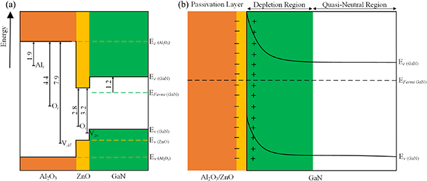
Figure 1. Band alignment between the thermodynamic energy levels of the native point defects in Al2O3 and ZnO, and the band edges in GaN: (a) energy level position of different point defects and the Fermi level of the GaN; (b) band bending at the interface of the passivation layer and GaN layer, and formation of a depletion region and an electric field. Energies in eV.
Download figure:
Standard image High-resolution imageThe charge transport mechanism in the GaN LEDs with and without the proposed double-layer Al2O3/ZnO passivation layer is shown in figure 2. The electric field is formed at the interface of the passivation layer and GaN layer. The directionality of the electric field keeps the free negative charge carriers away from the surface of the semiconductor and prevents them from being trapped there. This can reduce the non-radiative recombination of the charge carriers, decrease the shunt leakage current, and improve the optical and electrical properties of the GaN LED.
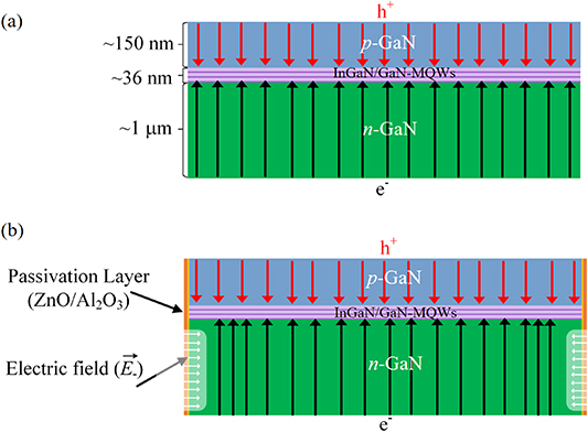
Figure 2. Charge transport mechanism in GaN LEDs (a) without and (b) with field-effect passivation layer. The electric field keeps the free negative charge carriers in n-GaN away from the high recombination surface areas.
Download figure:
Standard image High-resolution imageIt should be noted that the proposed field-effect passivation is more effective in the n-GaN region compared to p-GaN, and therefore, its effect will be primarily investigated in the present work with respect to this layer. In other words, the electric field that is formed at the interface of the passivation and n-GaN layer repels the free electrons from getting close to the sidewall. On the other hand, the electric field that is formed at the interface of the passivation layer and p-GaN, may lead to attraction of free holes in p-GaN layer toward the sidewall region. However, the net positive effects of the proposed field-effect passivation at the n-GaN layer in reducing the non-radiative recombination outweighs the possible adverse effects of this approach at the p-GaN sidewall region [26, 27]. This is mainly due to a higher total of number of surface defects in n-GaN along with a much larger thickness of this layer compared to p-GaN.
3. Experimental
Figure 3(a) shows the schematic cross-section structure of the field-effect passivated GaN LED, which consists of a 1 µm n-type GaN layer with Si concentration of ∼3 × 1018 cm−3, three periods of InGaN (well: 20 Å)/GaN (barrier: 100 Å) quantum wells as the active region, and a 150 nm p-type GaN layer with elemental Mg concentration of ∼2 × 1019 cm−3, all grown using MOCVD on single-side polished sapphire substrate. A thin film of nickel oxide was used as the transparent conductive oxide layer for the purpose of current spreading on the p-GaN layer. The layout of the epi-wafer with LED chip dimension of 350 µm × 350 µm is shown in figure 3(b). Further details regarding the fabrication process and the basic electrical and optical characterization of the LEDs are described elsewhere [28–30].
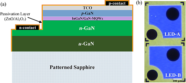
Figure 3. (a) Schematic cross-section structure, and (b) cathodoluminescence microscope image of the GaN LEDs used in the present work. The layout of the GaN epi-wafer with LED dimension of 350 µm × 350 µm.
Download figure:
Standard image High-resolution imagePrior to deposition of the double-layer Al2O3/ZnO passivation layer, the samples were first rinsed in acetone and methanol to remove the organic contaminants and were then blow-dried using clean dry air and high purity nitrogen. Following that, the samples were directly transferred to the ALD chamber to minimize the possibility of cross contamination. The Al2O3/ZnO thin films were deposited on the sidewall surface of the GaN LEDs using the GemStar XT thermal ALD system at a substrate temperature of 200 °C, base pressure of 50 mTorr. High purity nitrogen (99.999%) was used as the carrier gas with a flow rate of 40 sccm.
Trimethylaluminum (TMA) and diethylzinc (DEZn) were used as the metalorganic precursors along with DI water as the oxidizing agent for deposition of the Al2O3 and ZnO films during the ALD growth process. The pulse/purge times for the precursors were optimized to 20 ms/6 s for TMA and 200 ms/6 s for the DEZn in order to achieve a growth rate per cycle of 1.16 Å/cycle for Al2O3 and 1.80 Å/cycle for ZnO.
The actual thickness of the samples was measured using J.A. Woollam optical ellipsometer (incident angle: 75°, measurement data fit to Cody–Lorentz optical model) and confirmed to be ∼18 nm for Al2O3 and ∼2 nm for ZnO, resulting in a total thickness of ∼20 nm for the double-layer stack [12, 31, 32]. High-resolution transmission electron microscopy (HRTEM) was carried out using FEI Tecnai 20 system with an accelerating voltage of 200 kV. Figure 4(a) shows the HRTEM image of the ALD-grown Al2O3/ZnO passivation layer, in addition to its corresponding fast Fourier transform (FFT) pattern, figure 4(b). It confirms an amorphous structure for the deposited passivation layer.
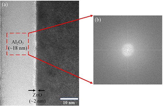
Figure 4. (a) HRTEM image of the ALD-grown Al2O3/ZnO passivation layer, (b) FFT pattern that shows the amorphous structure of the deposited passivation layer.
Download figure:
Standard image High-resolution imageIn order to study the effect of the ALD-Al2O3/ZnO field-effect passivation on the GaN LEDs, four devices from the wafer, named LED-A, LED-B, LED-C, and LED-D, were examined. The diode-like properties of these LEDs were characterized using the I–V measurements. The data acquisition for this measurement was carried out by the means of a Keithley 2400 automated sourcemeter in dark conditions and at room temperature. The measured data were fitted to the Shockley diode equation to derive the forward voltage, shunt resistance, and the ideality factor.
4. Results and discussion
The I–V characteristics of the two best performing devices, LED-A and LED-B, before and after using the Al2O3/ZnO passivation layer, are shown in figure 5. The inset in figure 5 shows the optical microscope image of the devices operating at the applied bias voltage of +5 V. The forward voltage (VF), which was measured at the forward driving current of 20 mA, did not exhibit a notable change in either device, and remained constant at ∼4.5 V before and after passivation. This demonstrates that the Al2O3/ZnO passivation layer did not affect the operating voltage of the devices.

Figure 5. I–V characteristics of (a) LED-A and (b) LED-B before and after using the ALD-grown Al2O3/ZnO double-layer passivation layer. Inset shows the optical microscope image of the blue GaN LEDs operated at the applied bias voltage of +5 V. Devices do not have heat sink.
Download figure:
Standard image High-resolution imageOn the other hand, the reverse leakage current (ILeakage), which was measured at −0.5 V, shows a significant reduction from 3.34 nA and 0.99 nA before passivation to 70.52 pA and 213.76 pA after passivation for LED-A and LED-B, accordingly. The lower ILeakage suggests the effectiveness of the proposed field-effect passivation layer in both reducing the density of the active surface states and lowering the non-radiative recombination of free charge carriers along the mesa sidewall.
Figure 6 shows the changes in parasitic resistance versus the applied voltage for LED-A and LED-B before and after passivation. The value of the shunt resistance (Rsh) for both devices was extracted by calculating dV/dI when the applied voltage is well below the forward voltage. This parameter describes the shunt conduction paths that are caused by the surface defects, and it directly affects the total leakage current. The Rsh for both LEDs is notably increased after the field-effect passivation. This indicates a reduction in the leakage current and improvement in the electrical properties of the passivated GaN LEDs.

Figure 6. Parasitic resistance versus the applied voltage for (a) LED-A and (b) LED-B. The value of shunt resistance (Rsh) was extracted by calculating dV/dI when the applied voltage is well below the forward voltage.
Download figure:
Standard image High-resolution imageThe series resistance (Rs) and the ideality factor (n) of the devices can be extracted from the I–V characteristics at above the forward voltage region. The differential form of the standard Shockley diode equation can be used to derive these parameters, which can be described as
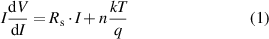
where Rs is the series resistance, n is the ideality factor, and kT/q is the thermal voltage at 300 K, equivalent to 0.0259 V [33]. The I·dV/dI versus I plot for LED-A and LED-B is shown in figure 7. A linear fit was used to extract the n and Rs of the GaN LEDs, in which it was applied to diode forward current range of more than 10 mA. The insets in figure 7 show the forward semi-log I–V curves, in which a linear current–voltage behavior is observed for applied voltage greater than the forward voltage.

Figure 7. Plots for I·dV/dI versus I for (a) LED-A and (b) LED-B, before and after field-effect passivation. A linear fit was applied to current range above 10 mA. The insets show the semi-log I–V curves, which exhibits a linear current–voltage behavior above the forward voltage.
Download figure:
Standard image High-resolution image
Table 1 shows the summary of the extracted electrical properties of the two best performing devices (LED-A and LED-B) along with the average performance of all devices (LEDs-A–D). A reduction in n was observed from 8.54 and 8.02 before passivation to 5.18 and 5.23 after passivation for LED-A and LED-B, accordingly. This is mainly because of the decrease in the process of non-radiative recombination, which itself stems from the field-effect passivation. It should be mentioned that the main reason for observed high ideality factor (≫1) both before and after passivation is because of the polarization-induced triangular band profiles of undoped quantum barriers (QBs) inside the InGaN/GaN MQWs active region. The ideality factor of the devices can be further reduced by increasing the number of intentionally doped QBs in the active region of the device [34]. Moreover, a slight increase in the forward current (IF), which was measured at the forward applied bias voltage of 5 V, was observed after passivation. This can likely be attributed to decrease in the ideality factor of the devices after the passivation.
Table 1. Extracted electrical parameters of LED-A and LED-B before and after Al2O3/ZnO field-effect passivation.
| VF a (V) | IF b (mA) | ILeakage c (pA) | n | Pout (mW) | Rs (Ω) | ||
|---|---|---|---|---|---|---|---|
| LED-A | No Passivation | 4.53 | 27.78 | 3334.32 | 8.54 | 125.84 | 56.24 |
| Al2O3/ZnO Passivation | 4.50 | 28.81 | 70.52 | 5.18 | 129.65 | 60.76 | |
| LED-B | No Passivation | 4.54 | 27.93 | 993.28 | 8.02 | 126.80 | 50.15 |
| Al2O3/ZnO Passivation | 4.49 | 29.41 | 213.76 | 5.23 | 132.05 | 58.18 | |
| Avg. (LEDs-A–D) | No Passivation | 4.54 | 26.78 | 1118.49 | 7.90 | 126.46 | 52.18 |
| Al2O3/ZnO Passivation | 4.48 | 27.94 | 88.46 | 6.25 | 130.48 | 54.93 | |
a Measured at forward driving current of 20 mA. b Measured at forward applied voltage of 5 V. c Measured at reverse applied voltage of −0.5 V.
The observed increase in Rs is likely due to increased probe resistance after ALD deposition of the Al2O3/ZnO passivation layer on the whole surface of the LED devices. In other words, formation of a metal–insulator–metal structure is likely to occur between the probe needle and the p-contact metal, which could result in a slight increase in the series resistance. This issue can be eliminated by formation of a via opening on the p- and n-contact metals, in which the probe needle directly connects to the contact metal.
It can be concluded from table 1 that the overall characteristics of LEDs, averaged across all four devices, follow a similar trend with the two best performing devices. In other words, introduction of the Al2O3/ZnO field-effect passivation layer has led to an improvement in diode-like properties of the devices, especially a notable decrease in the leakage current, as well as an increase in the output power (Pout) and the parasitic shunt resistance.
5. Summary and conclusions
In conclusion, the field-effect passivation of blue GaN LEDs were studied. Ultrathin films of Al2O3 and ZnO, with the thicknesses of ∼18 and ∼2 nm, were deposited on the sidewall surface of the LEDs using the ALD technique at the substrate temperature of 200 °C. The imbalance in charge neutrality at the interface of the passivation layer and active semiconductor layer, which is mainly caused by the negative fixed charge centers close to the top surface of the Al2O3/ZnO layer, is expected to form an electric field. The directionality of this electric field keeps the free negative charge carriers away from the surface of the semiconductor and prevents them from being trapped at the surface defects. Electrical characterization of the LEDs before and after using the passivation layer revealed a significant reduction in the leakage current, in addition to an increase in the parasitic shunt resistance for the passivated devices. This enhancement in the performance of the passivated devices is likely due to a reduced rate of non-radiative recombination of free electrons at the sidewall surface of the n-GaN layer.
Acknowledgments
The authors would like to acknowledge the technical support received throughout this work from the Material Research Center (MRC) at Missouri S&T in characterizing the ALD-grown thin films.
Data availability statement
The data that support the findings of this study are available upon reasonable request from the authors.