
Abstract
III-nitride quantum dots are proving to be promising for application to single photon emitting devices. Research around the globe is revealing several interesting properties of these emitters, including a wide range of emission wavelengths, high temperature operation, and deterministic polarization of the emitted photons. Here a review is given on the single photon emission properties of such III-nitride quantum dots.
Export citation and abstract BibTeX RIS

Original content from this work may be used under the terms of the Creative Commons Attribution 4.0 licence. Any further distribution of this work must maintain attribution to the author(s) and the title of the work, journal citation and DOI.
1. Introduction
Single photon emitting devices are set to play a major role in the realization of many quantum technologies, such as quantum communication systems and optical quantum computers [1]. The emitter will ideally provide a pure stream of individual, indistinguishable, photons on demand (or at a high emission rate), which will then be operated on with various downstream optical elements/circuits [2]. Room temperature operation (of both the emitter and detection systems) is also desirable for practical operation to negate the need for cumbersome and costly cryogenic cooling systems. In recent years much progress is being made in the development and investigation of such emitters, including studies on various material systems and emitter architectures. Indeed, as the scientific community continues to explore the properties of various materials, single photon emission has now been reported from a wide range of systems, including single trapped atoms [3–5] and ions [6, 7], nitrogen vacancy centers [8] in diamond, other similar defects [9], organic molecules [10], carrier localization centers housed in 2D materials [11–14], and from semiconductor quantum dots (QDs) [15–21]. In this review article we focus on and discuss the development of QD based single photon emitters made from the III-nitride material system.
In principle a QD can be defined as a localized region of space in which charges can be electrically confined such that the energy levels become quantized with a zero-dimensional density of states [22]. Typical QD sizes are on the order of a few nm. This quantization facilitates the realization of a quantum two level system for trapped charge carriers, the transitions between which allow for the emission of individual quanta of light [19]. Solid state semiconductor QDs are formed by an inclusion of a material of a lower bandgap surrounded by a material with a larger bandgap, such that electrons and holes can be confined in the lower-bandgap material. Many material systems have been investigated for the development and control of QDs, and, similar to other material systems, several methods have been developed to realize such structures in the III-nitrides [23–27], via both epitaxial growth or post growth sample processing. Accordingly, there have been several types of III-nitride QD geometries used to realize single photon emission, including dots that form via strain relief during epitaxial growth (so called self assembled QDs) [28, 29], QDs formed in larger structures such as nanowires [30–34] and nano/micro-pyramids [35, 36], QDs formed in quantum well thickness fluctuations [37], and QDs formed by local fluctuations in material composition. Figure 1 presents a selection of some typical QD structures realized with III-nitrides.

Figure 1. Comparison of different III-nitride QD geometries. (a) Self assembled GaN QDs typically form as truncated hexagonal pyramids [28]. Copyright (2006) Springer Nature. (b) Nanowire quantum dots forming at the apex of pencil-like nanowires. Reprinted with permission from [38]. Copyright © 2014, American Chemical Society. (c) Interface fluctuations of a quantum well. Reprinted with permission from [37]. Copyright © 2017, American Chemical Society. (d) QDs formed in the center of nanowires for electrical contacting [31]. Copyright © 2013, Springer Nature. With permission of Springer. (e) Quantum dots formed on non-polar surfaces of hexagonal nanowires. Reproduced from [39]. CC BY 4.0.
Download figure:
Standard image High-resolution imageAmongst other material systems typically studied for application to quantum light sources, the III-nitride material system stands apart as it is heavily used on an industrial scale for solid state lighting applications, and thus benefits from a large scale infrastructure for device manufacture and processing. In addition to this, there are two key reasons why III-nitride materials represent a solid choice for the future development of single photon emission technologies: Emission at relatively high temperatures is possible, and emission over a wide range of wavelengths can be obtained. These properties stem from the wide range of direct band gaps available from the materials (AlN: ∼6 eV, GaN: ∼3.4 eV, InN: ∼0.65 eV), which cover the whole of the visible region of the electromagnetic spectrum, in which relatively cheap and efficient, room-temperature operating, single photon detectors are readily available. To date single photon emission from GaN/AlGaN and InGaN/GaN QDs has been confirmed at wavelengths ranging from as low as ∼285 nm [38] to as high as ∼620 nm [40]: spanning from the deep ultra violet to the red region of the visible spectrum. In principle it is possible to further extend this wavelength range to telecommunications band wavelengths in the infrared by using InN-based structures [41]. Whilst emitters operating in the telecommunications band will be required for the realization of long distance quantum communication technologies such as fibre-based quantum key distribution [42], single photon emission in the visible and UV regions could be used for short range applications, such as on-chip linear optical quantum computing [1, 43], where the wide bandgaps of III-Nitrides would also allow for optical transparency.
Other required properties [44] of single photon emitters include fast operation rates (∼GHz), high efficiencies, and high emission purity. In addition to these properties, room temperature operation will be desirable for practicably useable devices, and indistinguishability of each successive emitted photon will be required for applications requiring two-photon interference, such as optical quantum computing.
In the following sections we provide a review on the single photon emission properties of III-Nitride QDs, focussing mainly on experimental demonstrations of single photon emission. In section 2 we outline some general aspects of the optical properties of III-nitride QDs, focussing on emission lifetimes, spectral diffusion, emission polarization, and biexciton binding energies. We then discuss the reports of single photon emission from III-nitrides, particularly those with high emission purity (3.1), and those at high temperatures (3.2), respectively. Finally a brief summary and outlook are given.
2. Basic emission properties and material considerations
III-nitride materials are complex with many interesting features. They can crystalize in either the Wurtzite or Zinc Blende crystal structure. Of these two, Wurtzite is the more easily formed, and to date the majority of studies on single photon emission in III-nitride QDs have been performed on Wurtzite structures. One aspect of this crystal structure, that has far reaching implications on the QD optical properties, is its non-centrosymmetric nature: it is a piezoelectric material.
As the lattice constants of the two materials that make up the QD and the barrier material, respectively, are usually different, coherent growth necessitates that strain be introduced into the system as one or both of the materials undergoes compression/expansion to minimize the total crystal energy. This strain leads to the presence of a strong internal electric field in III-nitride QDs, of order ∼ MV cm−1 [45], which acts to spatially separate the QD-confined electrons and holes [46–49], increasing the emission lifetime [50] and leading to the presence of a strong permanent dipole moment within the dot [51, 52]. Many attempts have been made to overcome these issues, including growth on semi-polar/ non-polar growth planes, and also using the Zinc–Blende crystal structure, as will be discussed in the following sections.
As mentioned in the introduction—the wide range of available bandgaps in the III-nitride system enables emission over a wide range of wavelengths; a fact which gives this material system the status of being the only system discovered to date that is capable of covering the UV to the IR. However it is important to note that, depending on the crystal orientation, the piezoelectric field can also act to strongly shift the emission such that the size of a given dot will have a large effect on its exact emission energy [53]. Furthermore, in the case of ternary compounds, such as InGaN, compositional fluctuations have also been shown to lead to a wide range of emission energies [54].
2.1. Emission lifetimes
Due to aforementioned electric fields present in III-nitride nanostructures, the confined electrons and holes become spatially separated leading to long emission lifetimes through the quantum confined Stark effect (QCSE). The emission lifetime dependence on the QD size has been well documented [50, 53, 55], and in the case of GaN QDs, lifetimes that vary over a few orders of magnitude (from greater than 1μs to less than 1 ns) have been measured, along with a change in the emission energy from ∼2.5 eV to ∼4.5 eV (see figure 2). Long emission lifetimes will ultimately limit the rate at which photons can be generated from a single quantum emitter, and therefore significant research effort has been made to overcome the QCSE and achieve more efficient carrier recombination. Methods that have been tried to date include using growth on semi-polar [56–58] or non-polar [39, 59–61] crystal planes, growing QDs in the ZB crystal phase [62–64], and using small QDs [53, 65]. Each of these methods has resulted in the realization of QDs with sub-nanosecond emission lifetimes, suggesting that single photon emission at rates of up to a few GHz may eventually be possible when using systems with high photon extraction efficiencies. Recently, methods to suppress the internal field via the generation of an opposing field are also being developed [66]. Other studies have shown that it is possible to use the strength of the internal field [67] to tune the QD emission energy over ranges of ∼60 meV, which may prove to be very useful for tuning III-nitride QDs into and out of resonance with photonic crystal cavities.

Figure 2. Measured radiative decay times as a function of emission energy for GaN quantum dots. Smaller dots emit at high energies and have drastically reduced lifetimes due to suppression of the quantum confined Stark effect. Reprinted from, with the permission of AIP Publishing.
Download figure:
Standard image High-resolution image2.2. Spectral diffusion and emission linewidths
III-nitride QDs typically exhibit a pronounced spectral diffusion in their emission spectra. This phenomenon occurs due to electronic interactions between the exciton confined in the dot, and other itinerant and trapped charges in the environment surrounding the dot. Unstable emission of any kind is, of course, undesirable, but spectrally fluctuating emission will cause significant problems with the generation of indistinguishable photons, as photons will become distinguishable by their differing energies.
Spectral diffusion occurs on several different timescales, and is often observed as unstable emission lines [63, 68–70], spectral jumps [71], and also broadened emission linewidths [52, 72, 73] (when the diffusion occurs on timescales faster than the spectral acquisition time). This phenomenon has been observed in many other material systems [74–80], but it is particularly strong in III-nitride QDs due to the internal-field induced excitonic permanent dipole moments, which interact strongly with charge fluctuations in the immediate environment of the QD. Although the exact nature of the charge traps that give rise to the spectral diffusion has not been elucidated, it is likely that they consist of both point and extended defects in the crystal, nearby QDs, surface states, and other localization centers such as local composition fluctuations. Examples from the literature of spectral diffusion occurring on different timescales can be found in figure 3.

Figure 3. Examples of spectral diffusion occurring on different time timescales in III-nitride quantum dots. (a) Spectral diffusion in InGaN/GaN QDs occurring on second timescales. Reprinted from [68], with the permission of AIP Publishing (b) Discrete spectral jumps in the emission energy of a GaN QD occurring on timescales of ∼10 s. Reprinted figure with permission from [71], © 2006 American Physical Society. (c) Fast spectral diffusion in GaN/AlGaN QDs occurring on timescales of ∼20ns, measured by photon autocorrelation (here the antibunching shows the single photon emission, and the longer timescale bunching effect reveals the timescale of the spectral diffusion). Reproduced from [73]. CC BY 4.0.
Download figure:
Standard image High-resolution imageFast spectral diffusion will cause the emission line to take on a more-or-less Gaussian profile (due to the stochastic nature of the fluctuating electronic environment). The linewidth of an emission line undergoing fast spectral diffusion will be determined by the strength of the Coulomb interactions between the confined charge and the charge in the environment, and also the distribution of traps in the vicinity of the dot [72]. Broadened emission lines in III-nitride QDs (particularly GaN QDs) have been reported with linewidths of several meV [52], even when the samples are cryogenically cooled to liquid helium temperatures. These linewidths are several orders of magnitude broader than what would be expected from purely lifetime broadened emission (which would exhibit a Lorentzian lineshape). Initial measurements of the timescales of the fast environmental fluctuations that give rise to this spectral diffusion in GaN QDs reveal timescales of tens of nanoseconds [73].
Despite this often-observed strong broadening of the emission line, there have been some reports of the measurement of narrower linewidths. For example, GaN QDs emitting in the deep UV with energies of >4 eV have been shown to exhibit linewiths of ∼590 μeV [81] and ∼440 μeV [82]. On the other hand, InGaN QDs have been regularly reported with spectral diffusion limited emission linewidths of a few hundred μeV [68, 83–85]. Still, these values are much broader than what would be expected due to purely lifetime broadening. Indeed, in the absence of spectral diffusion, for temporal processes occurring on timescales of ∼1 ns, we should expect homogeneously broadened linewidths roughly on the order of ∼1 μeV.
Recent advances in the growth of III-nitride QDs have led to reports of increasingly narrow emission linewidths. GaN/AlGaN quantum well interface fluctuation QDs [37] have been reported with linewidths as low as 87 μeV (from which an upper limit to the homogeneous broadening of the QD of 27 μeV was extracted). For these QDs the carrier confinement occurs at macro step regions at the periphery of hillock structures that form around a central open core dislocation during growth. The macro steps in the quantum well (that conforms with the profile of the hillock) lead to additional lateral confinement in the well. It is theorized that higher temperature growth used for these samples results in a cleaner environment with a lower density of charge traps [37, 86] than traditional GaN/AlN QDs. This lower density of defects ultimately leads to reduced spectral diffusion. Recent studies on InGaN/GaN QDs in nanopyramids also reported spectral diffusion limited linewidths as low as ∼160 μeV, from which a Lorentzian component homogeneous linewidth of 64 μeV was extracted [87].
Whilst these recent studies in estimating the homogeneous linewidths of III-nitride QDs no doubt mark great progress, the fact remains that the emission spectra are still dominated by spectral diffusion, and this diffusion must be eradicated if these structures are to find application in future quantum technologies which require a high degree of coherence. However, we note that spectral diffusion itself is not likely to be detrimental for some applications, such as quantum key distribution using the BB84 protocol [42], that do not require indistinguishability.
2.3. Emission polarization
Photon emission with a well defined and high degree of linear polarization is often reported from III-nitride QDs. Studies suggest that this phenomenon arises due to a combination of the properties of the QDs themselves [58, 85, 88–90, 91, 92], such as in-plane anisotropy (of the confinement potential and/or strain field) and strong band mixing, and also factors due to the external environment of the dot [31, 34–36, 84] (the optical modes supported by the structure that contains the QD, etc). This property is beneficial for various applications, such as quantum key distribution using the BB84 protocol, which requires the emission of photons in one of 4 polarizations [42].
Interestingly, many groups have reported success in controlling this polarization, either via direct control of the QD shape by lithographic processes [93], by control of the symmetry of the housing structure [94], or by growth of the QD on non-polar crystal planes such that the emission is polarized parallel to certain crystal axes [60, 95]. Examples of this polarized emission in III-nitride QDs are shown in figure 4.

Figure 4. Examples of measured polarization of emission from III-nitride QDs. (a) linearly polarized emission from an InGaN/GaN QD grown on non-polar a-plane material. The degree of linear polarization is 0.8 and the measurement was performed at a temperature of 220 K. Reproduced from [60]. CC BY 3.0. (b) Low temperature measurement of linear polarization from the emission of a single Zinc–Blende GaN/AlGaN QD exhibiting a high degree of linear polarization of 0.98. Reprinted with permission from [91]. © 2006 American Physical Society.
Download figure:
Standard image High-resolution imageIn the cases mentioned above, the observed photon polarization arises, in effect, due to the relative suppression of emission polarized perpendicular to the measured polarization. However, for QDs of any material that exhibit a degree of anisotropy, it is usually the case that orthogonally polarized lines become split in energy, resulting in a fine structure splitting (FSS) in the emission. In the cases that FSS has been observed in III-nitrides, values ranging from ∼100 μeV [96] to as large as a few meV [37] have been reported. Theoretical studies suggest that even larger values of FSS are present in higher energy emitting smaller QDs [97], (although such splitting may be difficult to observe and identify in reality due to strong suppression of one of the emission lines) [88].
As an aside, we note that whilst the generation of strongly linearly polarized photons is desirable, the large suppression of one polarization negates the possibility of generating polarization entangled photons from the biexciton-exciton cascade process (although a vanishing FSS is also required for this [98]).
2.4. Emission from biexcitonic states
Extraction of single photons from a QD requires the isolation of the emission due to the recombination of a single exciton. However, when using high excitation powers it cannot be guaranteed that just a single exciton will be excited in the QD. Under the conditions that the biexciton state is also excited (2 excitons confined in the same dot), it is important to be able to spectrally isolate the emission related to the exciton recombination from the emission related to the biexciton → exciton transition.
The biexciton binding energy, ΔEXX, (that is, the difference in energy between the biexciton state and that of two individual non-interacting excitons, manifested as an energy separation of the two transitions), is therefore an important parameter for determining if a single transition can be spectrally isolated (particularly at high temperatures when the transition lines will be spectrally broadened by phonons to linewidths of ∼30 meV). The biexciton binding energy is determined by the mutual interactions (Coulomb, exchange, configuration etc) of the constituent electrons and holes [28, 99–102]. As the positions of the carriers are strongly determined by the internal electric field and the QD geometry, III-nitride QDs in particular exhibit a wide range of binding energies, including both negative and positive values. This trend was basically explained by Simeonov et al [103] when they considered the large repulsive interaction between the electrons which conjugate near the top surface of typical GaN QDs of truncated hexagonal geometry. Hönig et al went on to later develop a theory on the formation of hybrid biexcitons in GaN QDs [100] that more or less explains the trend fully. However, it should be noted that in reality the absolute shape of a given dot will have a large effect on the observable biexciton binding energy.
In figure 5 we collate and compare data on biexciton binding energies measured from single QDs for a few typically studied material systems (we note that extremely large biexciton binding energies in excess of 100 meV have been observed from ensembles of CuCl microcrystallites embedded in NaCl [104], but have not been directly observed from individual structures).
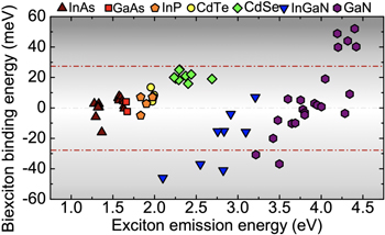
Figure 5. A comparison between biexciton binding energies for various material systems. The data was taken from [20, 28, 31, 33, 39, 51, 61, 65, 76, 85, 89, 103, 105–128]. The extent of biexciton binding energies observed from GaN QDs is immediately apparent when compared to those observed from other material systems.
Download figure:
Standard image High-resolution imageThe data in figure 5 reveals the large range of biexciton binding energies reported to date from III-nitride structures. Two dashed red lines have been added to the figure at energies of ±27 meV (kBT300K) as a guide for the eye. Inspection of figure reveals that there are two classes of GaN QDs that, due to possessing large absolute values of  meV, are likely to be allow for high temperature single photon emission: GaN QDs emitting at low energies (3–3.5 eV), and those emitting at high energies (4.2–4.5 eV). Indeed, these two energy regions are exactly the energy ranges in which high temperature single photon emission has been previously observed from GaN QDs: at 200 K from self-assembled QDs emitting at ∼3.5 eV [28], and at up to 350 K from site-controlled nanowire QDs emitting at ∼4.35 eV [32, 38]. Similarly, it is likely the case that InGaN QDs that emit at lower energies will be more suitable for high temperature single photon emission, in good agreement with the experimental results: to date 280 K emission at ∼2.1 eV [40], and 220 K at ∼2.5 eV [60]. These high temperature measurements will be discussed in the following section.
3. Single photon measurements on III-nitride QDs
Verification of single photon emission from an emitter is performed by measurement of the second order intensity autocorrelation at time delay τ
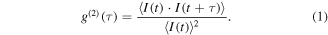
A measurement of antibunching in the photon autocorrelation with g(2)(0) < 0.5 verifies the presence of a single quantum emitter [44]. Pure single photon emission will exhibit perfect antibunching and yield a value of g(2)(0) = 0. The measurement itself is performed using a Hanbury Brown and Twiss setup, consisting of two photon detectors and a beam splitter. An emission peak selected for measurement is typically both spatially and spectrally filtered, and time intervals between detection events are then plot in a histogram to generate the g(2)(τ) function. The experiment can be performed using either pulsed or continuous excitation.
Single photon emission purity is one of the most important factors to quantify a single photon emitter, and is an area in which III-nitrides QDs have typically been lagging behind other, more developed, material systems. As mentioned above, g(2)(0) = 0 characterizes pure single photon emission, but in reality this is extremely difficult to achieve. However, it has been shown that g(2)(0) < 0.1 would be sufficient for some applications such as quantum key distribution, and g(2)(0) < 0.001 will be required for the realization of quantum repeaters and optical quantum computing [129]. In the following subsections we discuss the literature results on single photon purity, and high temperature emission from III-nitride QDs.
3.1. Single photon emission purity
Whilst it is generally believed that QDs can act as pure single photon emitters, experimentalists have to battle against background emission that contaminates the photon stream and degrades the measurable value of g(2)(0). In laboratory demonstrations of single photon emission, the contaminating emission typically arises from imperfect filtering of the measured emission from other centers that are spectrally and spatially close to the emitter under study. Background emission is usually a significant problem in III-nitrides (likely due to the high density of defects and other emission centers that are found throughout the samples), making it difficult to isolate and observe sharp emission lines free from any spectral contaminating luminescence. Indeed, many reports present results that reveal single photon emission of reasonable purity after the background emission has been accounted for in post experiment analysis. While such studies do reveal the single photon nature of the emission from the QD, it is important to note that the development of a useable source of single photons will require uncontaminated emission, and that it is the uncorrected raw value of g(2)(0) that is important for characterizing the purity of the photon emitter.
In order to suppress the background contamination and achieve single photon emission with the highest possible purity, the majority of studies are performed at low temperatures. However, even in these cryogenically-cooled conditions, many published results on III-nitride QDs still report g(2)(0) values greater than 0.1 [28, 32–34, 38, 39, 58, 60, 64, 82, 85, 87, 130–133].
Recently, however, g(2)(0) values as low as 0.02 have been measured from GaN quantum well interface fluctuation QDs [37] (see figure 6): the same emitters that are shown to have significantly suppressed spectral diffusion (see section 2.2). These results represent a large step forward in the development of III-nitride single photon emitters (perhaps even to the stage of useable devices), but even this low value is still far larger than recent reported values on the orders of 7.5 × 10⁻⁵ and 4.4 × 10⁻⁴ from arsenide [134] and arsenide/phosphide [135] materials (albeit obtained using advanced excitation and photon extraction methods). Further improvement of the single photon emission purity from III-nitride QDs can be expected via appropriate tuning of the excitation energy [136], and also resonant or quasi resonant optical excitation into the confined excited states [137–141] of the QDs.
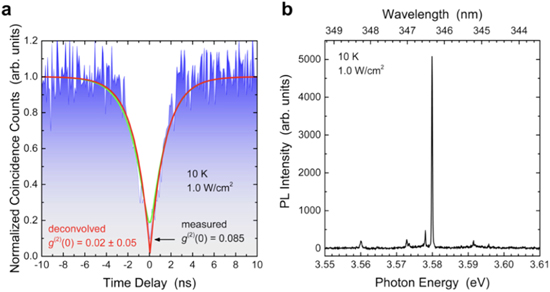
Figure 6. High purity single photon emission under continuous wave optical excitation from an interface fluctuation quantum dot exhibiting a g(2)(0) value of 0.02. The measurement was performed at a temperature of 10 K, and the emission spectrum shows very little background contamination emission. Reprinted with permission from [37]. Copyright © 2017, American Chemical Society.
Download figure:
Standard image High-resolution image3.2. High temperature operation
The possibility of single photon emission at high temperatures (facilitated by large band offsets and strong carrier confinement) has been one of our main motives for research into III-nitride based QDs. High temperature operation would negate the need for costly cryogenic cooling systems, and allow for device operation in environments such as on chips in computers and server systems. In the first published measurements of single photon emission from III-nitride QDs in 2005 [142], antibunched emission was measured at temperatures up to 70 K. This operational temperature was soon improved to 200 K [28]: which is significant technological importance as it is a temperature that can be reached by thermoelectric cooling. Further advances in understanding the thermal properties of III-nitride QDs were then achieved via the development of site-controlled nanowire GaN/AlGaN QDs [65]. These structures allowed a significant spatial isolation of individual quantum emitters with suppressed background contamination, and also exhibited large biexciton binding energies up to ∼50 meV. These properties allowed for the isolation and measurement of photon emission from the recombination of a single confined exciton at room temperature [38], and finally up to temperatures of 350 K (77 °C) [32]. See figure 7 for a measurement of g(2)(τ) from such a nanowire GaN QD at 350 K. These results were obtained with GaN/AlGaN based QDs that emit in the UV. However, high temperature single photon emission has also recently been achieved in the visible range of the spectrum via the use of InGaN/GaN QDs, from which single photon emission has been reported at temperatures up to 220 K for non-polar QDs exhibiting linearly polarized emission [60], and up to 280 K for QDs in a diode structure under direct electrical current injection [40].

Figure 7. A g(2)(τ) measurement showing single photon emission at an elevated temperature of 350 K from a single GaN nanowire quantum dot under pulsed optical excitation. Reprinted with permission from [32]. Copyright © 2016, American Chemical Society.
Download figure:
Standard image High-resolution image
It is important to stress here that higher temperatures in the system lead to increased phonon interactions, which in turn lead to broader emission linewidths. Indeed, for the case of GaN/AlGaN QDs emitting at room temperature and above, the observed emission consists of almost entirely phonon assisted recombination with a FWHM of 30–40 meV, and no discernible zero phonon line in the emission profile. Similarly, it has been shown that the InGaN QDs in nanowires at temperatures of ∼220 K exhibit linewidths [39, 60] of 20–40 meV. Such broad linewidths in principle do not directly affect the photon statistics as long as a single emission peak can be isolated, but will make the generation of indistinguishable photons difficult. Some studies have also shown that phonon interactions in III-nitride nanostructures are non-negligable even at cryogenic temperatures [143].
4. Summary and future outlook
Great progress has been made towards the development of III-nitride single photon sources in recent years. This has been achieved due to the collaborative research of many teams around the world. Advances have been made in realizing high temperature operation, emission with reasonable purity, and even deterministic photon polarization. However, there is still much work to be done. In particular, for such emitters to have a real impact in quantum information processing, it is necessary that the emission of indistinguishable photons [18] is realized. The development of such emitters will require higher crystal quality, and a hugely suppressed spectral diffusion. Additionally, the generation of entangled photons through a biexciton-exciton cascade [144] will require significant study into the FSS in III-nitride QDs. Although preliminary theoretical studies into such generation with III-nitrides have been performed [145], experimental verification has yet to be carried out.