
Abstract
Dopant diffusion of indium (In) in single crystal zinc oxide is studied by secondary ion mass spectrometry and is interpreted using a reaction–diffusion model that invokes predictions from density functional theory (DFT). An apparent activation energy of 2.2 eV is obtained for the diffusion of In, when the local Fermi-level position is about 0.2 eV below the conduction band edge. The diffusion of In is found to be significantly faster that that reported for the other group III donors, aluminum and gallium, with several orders of magnitude higher effective diffusivities, that can be assigned to a lower migration barrier for the diffusion of In. Furthermore, our results reveal self-consistency in previous DFT results of defect formation- and migration energies. From this, the diffusion of In is suggested to occur through mobile charged zinc vacancies  that form intermediate mobile (
 )− pairs. The pairs in turn dissociate rather readily at the studied temperatures (850 °C–1150 °C), which results in distinct and abrupt diffusion fronts for the In depth distribution profiles.
Export citation and abstract BibTeX RIS

Content from this work may be used under the terms of the Creative Commons Attribution 3.0 licence. Any further distribution of this work must maintain attribution to the author(s) and the title of the work, journal citation and DOI.
1. Introduction
Doping of zinc oxide (ZnO) with donor atoms, such as the group III elements aluminum (Al) and gallium (Ga) is common practice in realizing transparent conductive oxides (TCO) [1–4]. The main driver for using ZnO-based TCO's has been, and still is, the higher cost of the more commonly used indium-tin-oxide (ITO). ZnO is more abundant, and with reported resistivity as low as 8–9 × 10⁻⁵ Ω cm for Al- and Ga -doped ZnO [5, 6], i.e. comparable to that of ITO (7.2 × 10⁻⁵ Ω cm [4, 7]), makes ZnO desirable for use as a transparent electrode. However, for thin films (<100–200 nm) ZnO-based TCO's are still inferior to ITO in terms of resistivity stability at elevated temperatures in air ambience [3, 8]. In addition to Al and Ga, In has also been demonstrated to produce highly conductive ZnO layers, where a resistivity of about 8–9 × 10⁻⁴ Ω cm was reported for In-doped thin films prepared by spray pyrolysis [9] and RF magnetron sputtering [1]. This should be compared with a resistivity of 1.9 × 10⁻⁴ Ω cm and 5.1 × 10⁻⁴ Ω cm for Al- and Ga -doped ZnO, respectively, using similar magnetron sputtering deposition techniques [1]. Furthermore, it has previously been shown that self-compensation occurs in Al and Ga doped ZnO [10, 11], resulting in a conductivity limit and reduced applicability as TCO. The self-compensation was explained by the formation of doubly negatively charged zinc vacancies ( ) and a complex between
  and substitutional Al at zinc site (
 ) for Al-doped ZnO [11, 12]. Thus, given the similar valence character of In and its observed donor behaviour in ZnO,
  will presumably play an important role also in the case of In-doped ZnO-based TCO's.
Studies of donor dopant diffusion in ZnO enable information about the donor-defect interactions involved. Accordingly, such studies are a viable path to elucidate the mechanisms limiting the net carrier concentration. Previous experimental investigations of In diffusion in ZnO report activation energies ranging from 1.17 to 3.16 eV, with diffusion constants spanning over 9 orders of magnitude [13–15]. Clearly, this large inconsistency in literature data, including the dissimilar diffusion energies reported for two identical experiments, [13] and [14], urges the need for further studies of the In diffusion in ZnO.
In more recent years, calculations using density functional theory (DFT) have emerged as a method to estimate defect formation energies and also favourable migration paths for self- and impurity diffusion. Hence, by presuming a prevailing diffusion mechanism, DFT-calculations enable predictions of dopant diffusion activation energies. In the case of In diffusion in ZnO, a migration barrier for the prevalent ( pair has previously been predicted to be 1.22 eV (along the c-orientation), with an estimated overall diffusion activation energy of 1.77 eV under O-rich and n-type conditions [16].
In this work, we use secondary ion mass spectrometry (SIMS) to investigate the diffusion of In in single crystalline bulk ZnO, utilizing an effectively inexhaustible surface layer source. Similar to our previous reports on Al and Ga diffusion in ZnO [11, 17, 18], the experimental results are analyzed using a reaction–diffusion (RD) model that combines with DFT results from [16]. From this, we show that the formation- and migration energetics reported in [16] are self-consistent with our exeprimental results on In diffusion.
2. Method
2.1. Experimental
A thin film of In-doped ZnO ( ) was deposited onto hydrothermally grown single crystalline (0001-oriented) bulk ZnO (Tokyo Denpa), with a resistivity of 1310 Ω cm. The deposition was carried out in a Semicore magnetron sputtering system using an In-doped ZnO target (Zn0.95In0.05O) with a purity of 99.95%, resulting in a 0.3 μm thick In-doped ZnO film. After the deposition, the sample was sequentially heat treated for 30 min from 600 °C up to 1150 °C in stages of 50 °C to realize diffusion of In into the bulk crystal. A Cameca IMS7f SIMS equipped with a
  primary ion beam source was used to record the concentration versus depth profiles of In. Using a secondary ion field aperture, the circular gated region was 33 μm in diameter, ensuring a detected region only at the center of the 150 μm2 sputtered crater bottom. Absolute concentration values of In were obtained by measuring a In ion implanted reference sample, ensuring less than ±10% error in accuracy. For depth calibration, the sputtered crater depths were determined by a Dektak 8 stylus profilometer and a constant erosion rate was assumed. The sputter deposited films have been analysed by scanning transmission electron microscopy (STEM) imaging using a FEI Titan G2 60–300 at 300 kV with a convergence angle of 30 mrad, where the energy-dispersive x-ray (EDX) spectroscopy was performed using a Bruker Super-X quad detector. The STEM samples were prepared by conventional means of grinding and polishing.
2.2. Computational methods
2.2.1. Reaction diffusion model
To describe the experimental In diffusion depth profiles, a RD type model is employed that is based on a complete set of reaction diffusion differential equations (see e.g. [11, 17–22] for a similar and general treatment), and considers the formation, migration and dissociation of the ( pair through the following reaction

Here,  is highly mobile while
  is regarded as immobile at the studied temperatures. We can write the following system of RD equations for the migrating pairs

with Cs, Cp and Cv representing the concentration of substitutional In pairs and
  , respectively. ks is the dissociation rate of the pairs whilst
  is the corresponding formation rate. It was shown previously for Ga diffusion in ZnO [17] that when the transport capacity of
  is much higher than that of the pair (i.e.
  ), ks and kp are reduced to depend only on the binding energy of the pair and the effective radius (1 nm) for capturing
  by the substitutional dopant, respectively. In this regard, a pair binding energy of
  has been predicted by Steiauf et al [16], and is used as a fixed parameter in our simulations.
In order to solve the above RD equations (equations (2)), Cv(x, t) needs to be known. Profiles of Cv(x, t) can be estimated from DFT predictions of the  formation energy (
 ) and also accounting for the effect of band-gap narrowing at high temperatures. That is, the distribution of
  can be expressed as [11, 18]
where Ns is the number of substitutional zinc lattice sites, n equals  and accounts for the charge neutrality of the system, and Nc is the effective density of states in the conduction band. The high transport capacity of
  implies an almost instantaneous establishment of an equilibrium Cv that is governed by the local Fermi-level position. The vacancy formation energy can in turn be expressed by
  , where
  is the formation energy at the valence band edge, set to 7.0 eV in our simulations as guided by previous DFT reports [16, 23–25], and
  F is the Fermi-level position referenced to the valence band edge. At the simulated temperatures (900 °C–1150 °C), the band gap of ZnO (3.3 eV at 295 K) varies between 2.77 and 2.64 eV, assuming a similar temperature dependence for the band gap narrowing (−0.52 meV °C–1) as that reported up to 500 °C [26]. We further consider a fixed valence band edge, that is, the absolute value for the conduction band edge equates the band gap at all temperatures. For a more detailed discussion of the RD model used in this work, see [11, 17, 18].
2.2.2. Density functional calculations
First-principles calculations were performed by using the Heyd–Scuseria–Ernzerhof [27] hybrid functional and the projector augmented wave method [28–30], as implemented in the VASP code [31, 32]. The fraction of screened Hartree–Fock exchange was set to α = 37.5% [33], which yields a band gap (3.42 eV) and lattice parameters (a = 3.244 Å and c = 5.194 Å) that are in excellent agreement with experimental values [34, 35]. All defect calculations were performed using a plane-wave energy cutoff of 500 eV, a special k-point at  , and a 96 atom sized wurtzite supercell [25]. Defect formation energies were calculated by following the well established formalism outlined in [36, 37]. For instance, the formation energy of InZn in charge-state q is given by

where  and
and  denote the total energy of the defect-containing and pristine supercells, and μZn and μIn are the chemical potential of the removed Zn- and added In-atom, respectively. For charged defects, we applied the anisotropic [38] Freysoldt–Neugebauer–Van de Walle finite-size correction [39, 40]. Oxygen rich conditions are considered, where μZn corresponds to the total energy per bulk metallic Zn atom plus the formation enthalpy of ZnO, i.e.
  . The solubility of In is limited by the formation of In2O3, and under oxygen rich conditions
  .
.
3. Results and discussion
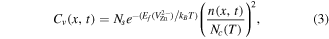
Figure 1 shows the In concentration versus depth profiles for the isochronally heat treated sample, as obtained from SIMS measurements. A migration of In from the In-doped ZnO film into the ZnO bulk is observable above 800 °C, while heat treatments conducted at lower temperatures (600 °C–800 °C) revealed no change in the In distribution. For treatments below 1150 °C, the In concentration in the 0.3 μm thick deposited film is over 2 orders of magnitude higher than the resulting apparent solid solubility of In in ZnO (i.e. the concentration of In at the bulk surface). At 1150 °C, In start to deplete from the film, but still holds a concentration that is one order of magnitude higher than in the bulk. The box shape of the In diffusion profiles are of similar character as that previously reported for Al [11] and Ga [17] in ZnO. However, as shown in figure 2, the apparent solid solubility of In is about one order of magnitude lower than that observed for Al and Ga at similar temperatures [11, 17]. In addition, the diffusion length of In is significantly longer than that of Al and Ga at comparable temperatures (see inset in figure 2), with the deep end of the In profile extending ∼11 μm after the 1050 °C treatment, as compared to ∼6 μm and ∼0.5 μm for Ga [17] and Al [11], respectively.
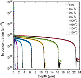
Figure 1. Experimental In diffusion depth profiles in ZnO. The solid lines show the best fit using the RD model for temperatures above 850 °C.
Download figure:
Standard image High-resolution image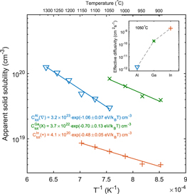
Figure 2. Comparison of apparent solid solubility for Al, Ga and In. The inset shows the corresponding effective diffusivities at 1050 °C, which have been calculated by equation (5). For Al and Ga, the data have been obtained from [11] and [17], respectively.
Download figure:
Standard image High-resolution imageFigure 3 shows the calculated formation energies of  , and substitutional
  ,
,  and
and  , versus the Fermi-level position. As seen, the formation energy of
  is higher than those of
  and
and  . The difference in the apparent solid solubilities between Al and Ga in figure 2 is in close agreement with that expected from the DFT results in figure 3; the calculated energy required to form
  is 0.23 eV higher than that of
  , which is consistent with the experimental values of (1.06 ± 0.07) eV and (0.70 ± 0.13) eV, respectively. Moreover, the pre-exponential factors for Al and Ga are close to the number of lattice sites in ZnO (
 Zn-sites), i.e. the extracted apparent solid solubility corresponds to the actual solubility. The absolute DFT values for Ef of
  and
and  in the studied temperature range (see figure 3) are also close to the experimental ones in figure 2, corroborating that the experimental ambient conditions (air) are close to that of the O-rich conditions in DFT. Further, from the DFT-data in figure 3, Ef of
  is expected to be 0.5 eV higher than that of
  . However, the apparent solid solubility of In (figure 2) does not corroborate this trend, but rather exhibit a lower value (by 0.6 eV) as compared to Al. Here, it should be noted that the pre-exponential factor obtained for In (figure 2) is significantly lower than that found for Al and Ga, and may indicate that the incorporation of In is limited by a different process. For instance, one possibility is that the rate of transport of In from the polycrystalline surface film and into the bulk crystal is the limiting process. Indeed, previous diffusion experiments [13, 14] using In ions implanted into ZnO samples reveal an In diffusion plateau with a concentration of
  already after annealing at 850 °C in air, which is notably higher than observed in our indiffused sample. On the other hand, even though the incorporation of In is transport limited, steady state surface conditions still apply, and the assumption of an inexhaustible diffusion source remains valid.
  may, however, be pinned slightly below the conduction band edge causing an increase of Ef(
 ) and thus also of the overall apparent diffusion activation energy.

Figure 3. Predicted formation energies as a function of Fermi-level position for Al, Ga and In dissolved at substitutional zinc site, and for  showing its various charge states. The dashed vertical lines indicate the estimated band gap/position of the conduction band edge at the elevated temperatures (900 °C and 1150 °C), estimated from [26] and used in the RD simulations.
Download figure:
Standard image High-resolution imageTo investigate the apparent transport limit in more detail, high-angle annular dark-field (ADF) imaging (HAADF) STEM analysis was conducted on the deposited In-doped film (after the 1150 °C treatment) and, for comparison, ADF imaging was conducted on the deposited Ga-doped film studied in [17] (after the 1050 °C treatment). Figure 4 shows the results obtained from the STEM analysis and reveal vertical lines of increased brightness for both the In- and Ga doped films. These lines may indicate the presence of inversion domain boundaries (see [41–44]) decorated with In and Ga, respectively. The observed contrast comes from the Z contrast that may be observed in ADF and HAADF. The appearance of the vertical lines are more frequent in the In-doped film, which could point to the fact that a larger fraction of In is trapped at inversion domain boundaries. If this is indeed the case, it may partly explain the limited flux of In from the deposited film as compared to the Ga-doped film. It can be noted that inversion domain boundaries have previously been observed for several elements in ZnO, including In [41, 42], Fe [41, 42], and Li [44] containing ZnO, and suggest that this is a rather common phenomenon in impurity doped ZnO. However, to fully understand this effect a dedicated study of the thin film-properties is needed, which is beyond the scope of this paper. It should also be noted that even though the lines in figure 4 are more frequent in the In-doped film, each line in the Ga-doped film seem to consist of several (3–5) atomic layers of Ga as compared to the single atomic layers observed for In.
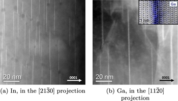
Figure 4. STEM images of the (a) In-doped ZnO deposited film after the 1150 °C treatment (HAADF) and (b) of the Ga-doped deposited film [17] after the 1050 °C treatment (ADF). The inset shows a higher magnification annular bright field image with the Ga Kα EDX signal overlaid.
Download figure:
Standard image High-resolution imageThe experimental diffusion profiles have been modelled using the RD model introduced in section 2.2.1, with the resulting best fits shown as solid lines in figure 1. The RD model with the migration barrier of ( as the controlling/limiting process for diffusion, closely reproduce the experimental profiles. In the simulations, only Cp and Dp are used as fitting parameters, where the former is treated as an influx boundary of already formed (
 pairs (formed in the film and 'injected' into the bulk crystal). Under equilibrium conditions and given that In mainly dissolve at substitutional zinc site, and that Cs ≫ Cp, the effective diffusivity can be expressed as (see [20, 21, 45]):

where  is taken as the apparent solubility
  and
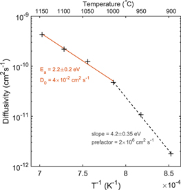
and  is the concentration of pairs at the bulk surface. Figure 5 shows the temperature dependence of Deff, revealing two different activated processes. At temperatures above 950 °C an apparent activation energy of
  with a diffusion constant of D0 = 4 × 10⁻² cm2 s−1 follows for the In diffusion. However, at lower temperatures the extracted diffusivities reveal a very different activated process. Since the diffusion prefactor is merely a structural entity [46],
  for ZnO (see e.g. [17]), the large prefactor of 2 × 106 cm2 s−1 obtained at low temperatures suggest that it does not represent a different diffusion mechanism, but may instead imply a transient diffusion behavior at these initial annealing stages. Indeed, as can be seen from the measured In concentration in figure 2, at the initial temperatures
  deviates slightly from the trend at higher temperatures, indicative of a transient regime. Therefore, only diffusion profiles above 950 °C is considered representative in the extraction of the In diffusion activation energy. Table 1 lists the present results together with those reported previously in the literature on the diffusion of In in ZnO.
Figure 5. Effective diffusivity versus inverse temperature. The solid line shows the best fit for  °C, while the dashed line shows the best fit in the temperature range 900 °C–1000 °C. Only the upper (solid) data is considered representative for the In diffusion activation energy, whereas the lower data (dashed) is discussed in terms of transient diffusion behaviour.
Download figure:
Standard image High-resolution image
Table 1.
Extracted diffusion parameter values for In in ZnO, together with previous theoretical and experimental results from the literature. With D0 being the pre-exponential factor, Em is the migration barrier for the exchange process of  and Ea is the apparent activation energy for diffusion.
| Type | D0 | Ea(In) | Em( )− )− |
|
|---|---|---|---|---|
| (cm2 s–1) | (eV) | (eV) | ||
| Present work | Exp | 4 × 10⁻² | 2.2 ± 0.2 | — |
| Thomas [15] | Exp | 2 × 10² | 3.16 | — |
| Sakaguchi et al [14] | Exp | 1.1 | 2.68 | — |
| Nakagawa et al [13] | Exp | 2.9 × 10⁻⁷ | 1.17 | — |
| Steiauf et al [16] | Theo | — | 1.77 | 1.22 |
In our simulations, only the product  is a unique quantity, and from experiments alone it is only possible to separate the two quantities in cases where (i) the pair is not the controlling/limiting process for the diffusion, or (ii) by isoconcentration experiments. Assuming that equation (1) is the prevailing diffusion mechanism, both (i) and (ii) would result in a shape of the diffusion profiles being very different from the present ones in figure 1, resembling that of erfc(x) functions [18, 20, 47]. However, as we have recently demonstrated for Al [18] and Ga [17] diffusion, it may be possible to separate Cp and Dp also at conditions different from (i) and (ii) by introducing DFT results to the RD-simulations (see section 2.2.1). In contrast to Al and Ga, applying the same procedure (as outlined in [17]) to determine Dp fails in the present case of In. This reveals an inadequacy of our RD model at these conditions, and may be due to the much lower dopant concentration in the present experiment. This may indicate that our RD simulations do not sufficiently account for the concentration and distribution of
  (equation (3)) in this somewhat moderate n-type conductive sample, and further experiments may be necessary to resolve it. Nonetheless, the extraction of
  (equation (5)) will not be affected and the determination of Ea(In) = 2.2 eV is still valid. It should be noted that since we could not determine Dp, similar results (
 ) can also be obtained using a much simpler approach, e.g. Fair's model (see [17]), instead of using a system of RD equations.
On the other hand, the overall diffusion processes can be approximated through [17]
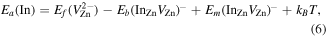
where the term kBT is about 0.1 eV at the studied temperatures. F is positioned about 0.2 eV below the conduction band edge, which combined with the DFT-results in figure 3 yield  values between 2.0–2.1 eV at the plateau of the In profiles during diffusion. Thus, using our extracted value of Ea = 2.2 eV (together with Eb = 1.19 eV) this gives
  , which is in excellent agreement with that predicted by DFT calculations (1.22 eV) [16], demonstrating self-consistency in the theoretical predictions by [16].
Interestingly, our In results differ from those reported previously by Thomas [15] (Ea(In) = 3.16 eV), Sakaguchi et al [14] (Ea(In) = 2.68 eV) and Nakagawa et al [13] (Ea(In) = 1.17 eV). It is, however, not obvious why the activation energy obtained by Sakaguchi et al [14] (2.68 eV) differs so much (1.5 eV) from that found by Nakagawa et al [13] (1.17 eV) performing nominally the identical experiment. It can also be noted that Nakagawa et al [13] report a surprisingly low pre-exponential factor, D0, of 2.9 × 10⁻⁷ cm2 s−1.
4. Conclusions
To summarize, we have studied the diffusion of In in single crystalline ZnO and found that it can be well described as mediated by  , through the intermediate formation and dissociation of (
 )− pairs. An activation energy of 2.2 ± 0.2 eV, with a diffusion constant of 4 × 10⁻² cm2 s−1 is obtained for the diffusion of In at temperatures 1000 °C up to 1150 °C. This is lower than that reported from previous experiments in the literature [14, 15], but is in good agreement with recent DFT results [16] when considering the somewhat moderate n-type conductivity in the present sample with a local Fermi-level position at ∼0.2 eV below the conduction band edge. Moreover, the theoretical predictions of Ef(
 ),
),  and
and  made in [16] are found to be self-consistent with our experimental In diffusion profiles.
Acknowledgments
We gratefully acknowledge the financial support from the Research Council of Norway for funding of the DYNAZOx-project (no. 221992), Salient (no. 239895) and NORTEM (197405/F50), and the University of Oslo for funding through FUNDAMENT (no.151131, Fripro Toppforsk program), and the Norwegian Micro- and Nano-Fabrication Facility (NorFab 245963).