

Abstract
(AlxGa1−x)2O3/Ga2O3 metal-oxide semiconductor field effect transistors are emerging as candidates for rf and power electronics, but a drawback is the high contact resistances on these wide bandgap semiconductors. A potential solution is to use narrower gap transparent conducting oxides such as IZO and ATO to reduce the interfacial resistance. In this paper, we report the measurement of the valence band offset of the AZO/(Al0.14Ga0.86)2O3 and ITO/(Al0.14Ga0.86)2O3 heterointerfaces using x-ray Photoelectron Spectroscopy. The single-crystal β-(Al0.14Ga0.86)2O3 was grown by molecular beam epitaxy. The bandgaps of the sputter-deposited AZO and ITO were determined by reflection electron energy loss spectroscopy to be 3.2 ± 0.20 and 3.5 ± 0.20 eV, respectively, while high resolution XPS data of the O 1s peak and onset of elastic losses was used to establish the (Al0.14Ga0.86)2O3 bandgap as 5.0 ± 0.30 eV. The valence band offsets were −0.59 eV ± 0.10 eV and −1.18 ± 0.20 eV, respectively, for AZO and ITO. The conduction band offsets were 1.21 ± 0.25 eV for AZO, and 0.32 ± 0.05 eV for ITO. Both were of the straddling gap, type I alignment on β-(Al0.14Ga0.86)2O3 and all the offsets are negative, consistent with achieving improved electron transport across the heterointerface.
Export citation and abstract BibTeX RIS
Introduction
β-Ga2O3 is under development for power switching and control electronics as well as solar blind UV detection [1–11]. The β polymorph of Ga2O3 has a bandgap of ∼4.8 eV and is commercially available in large diameter bulk and epitaxial form [1–3, 8]. The absence of p-type doping capability [12, 13] has led to a focus on vertical Schottky rectifiers and gate all-around FinFET-like devices which operate in accumulation mode in the on-state [1, 3–5, 7–10]. Additionally for lateral devices, the (AlxGa1−x)2O3/Ga2O3 heterostructure has been recently demonstrated using modulation doping of the barrier layer [14–21], as β-Ga2O3 is nonpolar. There is strong interest in these heterostructures involving β-(Al, Ga)2O3 monoclinic phase alloys, in which the bandgap can be varied from 4.8 to 6 eV [14–21]. Typically, the x value is between 0.12 and 0.18 in the alloys. One of the drawbacks of β-(AlxGa1−x)2O3/Ga2O3 heterostructures is the high contact resistances encountered when fabricating Ohmic contacts [14–20].
One potential method for reducing the contact resistance is to include a lower gap transparent conducting oxide as an interlayer between the metal and the wide bandgap semiconductor [22–27]. The most commonly used TCOs are indium tin oxide (ITO) and aluminum zinc oxide (AZO). Sputtered films of both of these materials have been reported as intermediary layers for forming Ohmic contacts on Ga2O3 [22, 25, 27]. The use of Pt/ITO bi-layers to β-Ga2O3 improved the Ohmic contact properties compared to Pt/Ti through formation of an interfacial layer with lower bandgap and higher doping concentration than the Ga2O3 [22]. AZO interlayers are also proven effective in lowering contact resistance of Ti/Au contacts on n-type, Si implanted β-Ga2O3. A specific contact resistance of 2.82 × 10⁻⁵ Ω cm2 was reported for annealing at 400 °C, while Ti/Au contacts without the AZO interlayer did not lead to Ohmic behavior [25]. The band alignment at the heterointerfaces is obviously critically important in determining the favorability of carrier transport [28–39]. Currently, there have been no reports for the band alignments of these TCOs on (AlxGa01−x)2O3.
In this paper, we report on the determination of the band alignment in the AZO/(Al0.14Ga0.86)2O3 and ITO/(Al0.14Ga0.86)2O3 heterostructures, in which the TCOs were deposited by sputtering onto (Al0.14Ga0.86)2O3 grown by molecular beam epitaxy (MBE). This alloy composition is typical of that used in heterostructure transistors. The valence band offset was obtained from XPS measurements [40] and by measuring the respective bandgaps of the TCOs, we obtained the conduction band offset in the heterostructures and determined the band alignment type.
Experimental
1.5 nm AZO or ITO was deposited by RF magnetron sputtering on the (Al0.14Ga0.86)2O3/Ga2O3 structures and thicker layers (150 nm) on quartz substrates at room temperature using 3 in. diameter composite ITO (In2O3/SnO2 90/10) or AZO (Al2O3/ZnO2 2/98 wt%) targets. The RF power was 125 W and the working pressure was 5 × 10⁻⁶ Torr in a pure Ar ambient. The DC bias on the electrode under these conditions is in the range of 30–40 V. Both thick (150 nm) and thin (1.5 nm) layers of the dielectrics were deposited to be able to measure both bandgaps and core levels on the β-(Al0.14Ga0.86)2O3. Hall measurements on the thick AZO films showed resisitivity of 7.4 Ω cm−1, carrier concentration of 1.78 × 1018 cm−3 and Hall mobility of 26 cm2 V−1 s−1. X-ray diffraction 2θ scans showed a (002) peak at 34.3°, indicative of a [001] preferred orientation with the c-axis perpendicular to the substrate, similar to previous reports [41]. The thick ITO, XRD showed peaks due to (400) and (222), indicating the coexistence of [100] and [111] textures [42, 43]. The resistivity was 2.6 × 10⁻¹ Ω cm, with Hall mobility of 19 cm2 V−1 s−1 and carrier concentration of 9 × 1016 cm−3. For substrate cleaning pre-deposition, the following rinse sequence was employed: acetone, IPA, N2 dry, and finally Ozone exposure for 15 min. These films were deposited onto epi (Al0.14Ga0.86)2O3 that was grown by MBE. The sample was grown by oxygen plasma-assisted MBE using a Ga flux of 6 × 10⁻⁸ Torr, Al flux of 2 × 10⁻⁸ Torr, an oxygen plasma power of 280 W and a chamber pressure of 1.2 × 10⁻⁵ Torr. Under these conditions it is possible to maintain the phase purity of the alloy [44]. These AGO (Al0.14Ga0.86)2O3 layers were doped with Si to produce an n-type carrier density of 1017 cm−3, with mobility of 180 cm2 V−1 s−1 at room temperature and were 55 nm thick. The donor concentration was determined by electrochemical capacitance–voltage profiling at a frequency of 740 Hz on calibration samples and the composition was determined by x-ray diffraction on these same samples [44]. These epitaxial layers were grown on top of Sn-doped (6.3 × 1018 cm−3) bulk β-phase Ga2O3 single crystal substrates (500 μm thick) with (010) surface orientation grown by the edge-defined film-fed growth method. The heterostructure samples are shown schematically in figure 1.
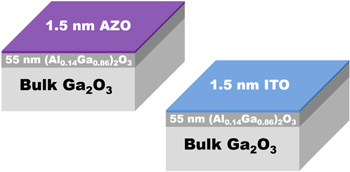
Figure 1. Layer structure of the heterostructures used in this work.
Download figure:
Standard image High-resolution imageThe chemical state of the ITO, AZO, and β-(Al0.14Ga0.86)2O3 and identification of peaks for high resolution analysis were obtained from XPS survey scans in a ULVAC PHI XPS system. This employs a monochromatic, Al x-ray source (energy 1486.6 eV) at a source power of 300 W. The analysis area was 10 μm in diameter with a take-off angle of 50° and an acceptance angle of ±7°. The electron pass energy was 23.5 eV for the high-resolution scans and 93.5 eV for the survey scans.
Charge compensation was achieved with a dual beam charge neutralization system with simultaneous low-energy electron and ion beams [45]. Using the position of the adventitious carbon (C–C) line in the C 1s spectra at 284.8 eV, charge correction was performed. During the measurements, the samples and electron analyzers were electrically grounded to provide a common reference Fermi level. Differential charging is a concern for semiconductor band offset measurements [45] and while use of an electron flood gun does not guarantee that differential charging is not present, our experience with oxides on conducting substrates has been that the differential charging is minimized with the use of an electron gun. Calibrations without the guns verified that was the case [36].
Reflection electron energy loss spectroscopy (REELS) was employed to measure the bandgap of the AZO and ITO [46]. By taking a linear fit to the leading plasmon peak and finding its zero energy with the background, a direct measurement of valence to conduction band energy is made. REELS spectra were obtained using a 1 kV electron beam and the hemispherical electron analyzer.
Results and discussion
Figure 2 shows the stacked XPS survey scans of thick (150 nm) AZO and ITO, 1.5 nm AZO and ITO on β-(Al0.14Ga0.86)2O3, and an (Al0.14Ga0.86)2O3 reference sample. There is no evidence of metallic contamination from the sputtering process, which if present in sufficient quantities can form oxides that reduce the overall bandgap of the dielectrics and affect the resulting band alignment [47–50].

Figure 2. XPS survey scans of thick sputtered AZO and ITO, 1.5 nm sputtered AZO and ITO on (Al0.14Ga0.86)2O3, and a (Al0.14Ga0.86)2O3 reference sample. The intensity is in arbitrary units (a.u.).
Download figure:
Standard image High-resolution imageWe obtained the valence band maximum (VBM) from linear fitting of the leading edge of the valence band and the flat energy distribution from the XPS measurements, and finding the intersection of these two lines [40, 49]. This is shown in figure 3 for the thick AZO and ITO, and the (Al0.14Ga0.86)2O3. The VBMs were measured to be 3.0 ±0.2 eV for β-(Al0.14Ga0.86)2O3, 2.53 ± 0.4 eV for the AZO and 2.74 eV ± 0.4 eV for the ITO.
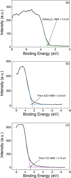
Figure 3. XPS spectra of core levels to valence band maximum (VBM) for (a) reference (Al0.14Ga0.86)2O3, (b) thick film sputtered AZO, and (c) thick film sputtered ITO. The intensity is in arbitrary units (a.u.).
Download figure:
Standard image High-resolution imageThe measured bandgaps for the AZO and ITO were 3.2 ± 0.30 eV and 3.5 ± 0.30 eV, respectively, from the REELS data of figure 4. The bandgap of the β-(Al0.14Ga0.86)2O3 was determined to be 5.0 ± 0.3 eV, from XPS O1s based electron energy loss measurements [40, 41]. This is consistent with past work on powdered samples of (AlxGa1−x)2O3 over the composition range x = 0–0.4 [51]. If we use the theoretical relationship derived by Peelaers et al [29], we would expect a bandgap of 5.14 eV at our composition of x = 0.14, close to the measured result. The difference in bandgaps between AZO and ITO and β-(Al0.14Ga0.86)2O3 are therefore 1.8 and 1.5 eV, respectively, and then it is necessary to determine how these are partitioned between valence and conduction bands.
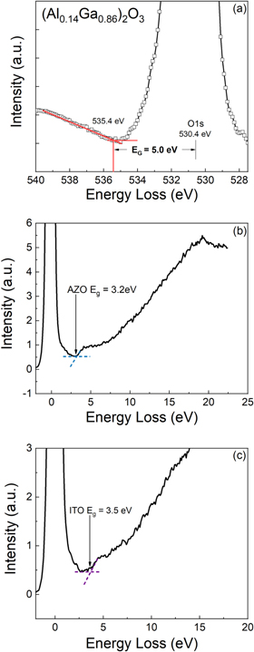
Figure 4. Bandgap of (a) (Al0.14Ga0.86)2O3 determined by the onset of energy loss spectrum. Bandgap of sputtered (b) AZO and (c) ITO determined by RHEELS data. The intensities are in arbitrary units (a.u.).
Download figure:
Standard image High-resolution imageTo determine the band alignment, we used the standard core level spectra approach due to Kraut et al [40]. This method relies on precise measurement of a core level and the valence band edge for each material investigated and the shift of the core levels when the two materials have formed the heterojunction. The equation used to calculate the offset is:

It is important to use a well-defined core level since the offsets are small compared to the core level energy and more deviation is expected at higher core level energies.
High resolution XPS spectra of the VBM-core delta region are shown in figure 5 for the β-(Al0.14Ga0.86)2O3 and thick AZO and ITO samples. These were used to determine the selected core level peak positions. Figure 6 shows the XPS spectra for the β-(Al0.14Ga0.86)2O3 to AZO and ITO core delta regions of the heterostructure samples. These values are summarized in table 1 and were then used to calculate ΔEv.
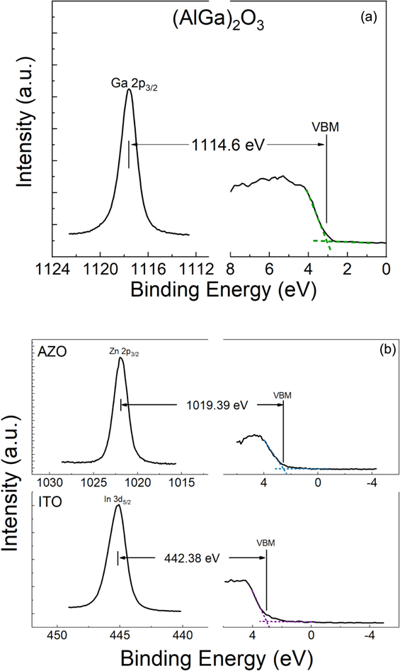
Figure 5. High resolution XPS spectra for the vacuum-core delta regions of (a) (Al0.14Ga0.86)2O3 and (b) sputtered AZO and ITO films. The intensity is in arbitrary units (a.u.).
Download figure:
Standard image High-resolution image
Figure 6. High resolution XPS spectra for the (Al0.14Ga0.86)2O3 to AZO and ITO core delta regions. The intensity is in arbitrary units (a.u.).
Download figure:
Standard image High-resolution imageTable 1. Summary of measured core levels in these experiments (eV).
| Reference (Al0.14Ga0.86)2O3 | Reference dielectric | Thin dielectric on (AlGa)2O3 | |||||||
|---|---|---|---|---|---|---|---|---|---|
| Core level | VBM | Core level peak | Core-VBM | Film (Core) | VBM | Core level peak | Core-VBM | Δ Core level | Valence band offset |
| Ga2p3/2 | 3.00 | 1117.60 | 1114.60 | AZO (Zn 2p3) | 2.53 | 1021.92 | 1019.39 | 95.8 | −0.59 |
| ITO (In 3d5) | 2.74 | 445.12 | 442.38 | 673.4 | −1.18 | ||||
Figure 7 shows the band alignment of the AZO/β-(Al0.14Ga0.86)2O3 and ITO/β-(Al0.14Ga0.86)2O3 heterostructures. Both are nested, type I systems. The valence band offset is −0.59 ± 0.10 eV and conduction band offset is −1.21 ± 0.25 eV for the AZO/β-(Al0.14Ga0.86)2O3. For the ITO/β-(Al0.14Ga0.86)2O3 heterostructure, the values are −1.18 ±0.20 eV for valence band offset and −0.32 ± 0.05 eV for the conduction band offset. These were obtained using the differences in bandgaps and the directly measured valence band offset, i.e.:  The band offsets are negative for both oxides on β-(Al0.14Ga0.86)2O3, ensuring good electron and hole transport and hence the ability to reduce contact resistance when used as an interlayer in metal stacks on this wide bandgap material.
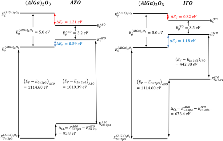
Figure 7. Band diagrams for the AZO (left) and ITO (right) sputtered onto (Al0.14Ga0.86)2O3. The valence band offset was determined to be −0.59 ± 0.08 eV for sputtered AZO and −1.18 ± 0.04 eV for sputtered ITO on β-(Al0.14Ga0.86)2O3. The conduction band offset was 1.21 ± 0.08 eV for AZO and 0.32 ± 0.04 eV for ITO on β-(Al0.14Ga0.86)2O3.
Download figure:
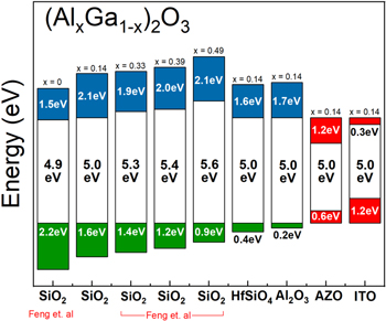
Standard image High-resolution imageTo place the work in context, figure 8 shows the reported values for band offsets of dielectrics on (AlxGa1−x)2O3. All of the reported values to date have been for oxides intended as gate dielectrics [30, 52, 53], which require a larger bandgap than the (AlxGa1−x)2O3 and typical need conduction band offsets of at least 1 eV to obtain good electron confinement. The work reported in this paper for AZO and ITO shows the negative offsets required for enhancing carrier transport across the heterointerface when used as an interlayer between the metal contact and the (AlxGa1−x)2O3.
Figure 8. Reported band offsets for various dielectrics on (AlxGa1−x)2O3 (data from 30] and our work [52, 53]).
Download figure:
Standard image High-resolution image
Summary and conclusions
The band alignment at both AZO/β-(Al0.14Ga0.86)2O3 and ITO/β-(Al0.14Ga0.86)2O3 heterojunctions is a nested gap (type I) band offset. The valence and conduction band offsets are negative in both cases, and can be used to enhance carrier transport across the heterointerface. The use of the AZO and ITO interlayers may be a convenient approach for improving Ohmic contact resistance on n-type β-(AlxGa1−x)2O3.
Acknowledgments
The project or effort depicted was partially sponsored by the Department of the Defense, Defense Threat Reduction Agency, HDTRA1-17-1-011, monitored by Jacob Calkins. The content of the information does not necessarily reflect the position or the policy of the federal government, and no official endorsement should be inferred.