

Abstract
In this paper, an approach for 3D plasma structure diagnostics using tomographic optical emission spectroscopy (Tomo-OES) of a nanosecond pulsed atmospheric pressure plasma jet (APPJ) is presented. In contrast to the well-known Abel inversion, Tomo-OES does not require cylindrical symmetry to recover 3D distributions of plasma light emission. Instead, many 2D angular projections are measured with intensified cameras and the multiplicative algebraic reconstruction technique is used to recover the 3D distribution of light emission. This approach solves the line-of-sight integration problem inherent to optical diagnostics, allowing recovery of localized OES information within the plasma that can be used to better infer plasma parameters within complex plasma structures. Here, Tomo-OES was applied to investigate an APPJ operated with helium in ambient air and impinging on planar and structured dielectric surfaces. Surface charging caused the guided streamer from the APPJ to transition to a surface ionization wave (SIW) that propagated along the surface. The SIW experienced variable geometrical and electrical material properties as it propagated, leading to 3D configurations that were non-symmetric and spatially complex. Light emission from He, N , and N2 were imaged at ten angular projections and the respective time-resolved 3D emission distributions in the plasma were then reconstructed. The spatial resolution of each tomographic reconstruction was 7.4 µm and the temporal resolution was 5 ns, sufficient to observe the guided streamer and the effects of the structured surface on the SIW. Emission from He showed the core of the jet and emission from N
 and N2 indicated effects of entrainment of ambient air. Penning ionization of N2 created a ring or outer layer of N
 that spatially converged to form the 'plasma bullet' or spatially diverged across a surface as part of a SIW. The SIW entered trenches of size 150 µm, leading to decreases in plasma light emission in regions above the trenches. The plasma light emission was higher in some regions with trenches, possibly due to effects of field enhancement.
Export citation and abstract BibTeX RIS
1. Introduction
Atmospheric pressure plasma jets (APPJs) typically consist of a non-thermal plasma (NTP) sustained by argon or helium propagating into ambient air. The NTP can produce large fluxes of UV radiation, charged particles, and reactive species, including OH, H, O, N, O3, and H2O2, while keeping the gas temperature near room temperature [1, 2]. Consequently, APPJs and interactions of NTP with surfaces offer opportunities for a myriad of temperature-sensitive applications such as wound healing [3], cancer treatment [4], polymer etching [5], water treatment [6, 7], agriculture [8], and catalysis [9, 10]. Realizing these applications requires understanding phenomena underlying interactions of NTP with the respective complex surfaces to optimize the desired kinetics.
Under the correct conditions, APPJs can produce stable ionization waves (IWs) that travel through a rare gas dominated channel surrounded by a less easily ionized gas [11, 12]. This process forms a plume at the outlet of the APPJ that is often referred to as a guided streamer. This plume mixes and reacts with the ambient air, however it can exhibit stable and reproducible behavior when operated periodically at kHz rates, likely due to significant seed electron densities [13]. This periodic operation leads to multiple IW fronts forming trains of plasma packets or 'plasma bullets' that propagate at velocities of up to  m s−1 within the rare-gas channel [14, 15]. In a process similar to streamer propagation, charge separation at the IW front and photoionization lead to electron avalanche in the gas which propagates the IW [16, 17]. When these guided IWs interact with a dielectric, they can become surface IWs (SIWs) that adhere to the surface due to charging of the dielectric generating electric field components parallel to the surface [18]. Local charging of the dielectric reduces the voltage drop across the IW front, weakening the SIW as it propagates until it dissipates. Applications typically involve non-planar surfaces with feature dimensions comparable to the dimensions of the SIW (
 m). For example, wrinkles and hair follicles on skin [3, 19], pellets, pores, and capillaries in catalytic surfaces [9, 10, 20], spices, seeds, and foodstuffs on decontamination beds [8, 21], and liquid droplets and particles on treated surfaces [22, 23], to name a few. Electric field enhancement at the apex of features and shadowing of ionizing radiation influence the SIW propagation, resulting in different exposure of the surface to the NTP [24].
APPJs have been well characterized with optical and laser diagnostics (see for example [1, 2, 12, 14, 25–27]), however SIWs present challenges. As the SIW adheres to the profile of the surface, optical measurement configurations must minimize or account for detection of light that is scattered or reflected from the surface, either from a laser source or the plasma itself [28]. The topography and material properties of the surface also need to be known or measured. Finally, SIWs form complex 3D plasma distributions [29, 30] that can be difficult to analyze. The distribution is often not axisymmetric, especially when considering non-planar surfaces, non-normal incidence of the APPJ, turbulent gas flow, or multiple interacting SIWs, and it is not possible to invert the distribution using the Abel transform [31, 32]. Laser-based diagnostics like those relying on laser-induced fluorescence (LIF) can provide localized information along the laser beam path and in 2D [33–35]. However, the spatial resolution is limited by the beam width (often  µm) and the full 3D distribution is not captured, limiting application to well-controlled and idealized plasmas where a 2D picture is sufficient for understanding phenomena of interest. Considering that SIWs on complex surfaces like tissue, liquids, polymers, plants, etc experience variable geometry, material properties, and gas composition that lead to complex 3D plasma distributions, modeling and diagnostic techniques that can provide a more complete 3D picture are needed.
In this paper, an optical tomographic reconstruction approach is presented for characterization of APPJs and SIWs. Multiple views of the plasma are acquired with a camera, and the line-of-sight integrated signals at each pixel are used to reconstruct the measurement volume. The ability to study the evolution of SIWs in 3D is evaluated using light emitted from metastable helium (Hem
) at 706.5 nm (33S to 23P), the first negative system of N at 391.4 nm (B
 to X
to X ), and the second positive system of N2 at 337.1 nm (C
 to B
to B ). These lines were chosen to reveal effects of air entrainment on the APPJ and SIWs propagating on planar and structured surfaces, as the interplay between the plasma and the ambient environment has a considerable impact on the physicochemical properties of the plasma and, therefore, on the application efficacy. As spectroscopic information is used, the approach is referred to as tomographic optical emission spectroscopy (Tomo-OES). Results revealed that Tomo-OES is suitable for volumetric reconstruction of guided streamers and SIWs with acceptable temporal (5 ns) and spatial (7.4 µm) resolution.
The optical tomography approach is similar to that implemented recently by Wang et al [36] to investigate vacuum arcs that deviated from axisymmetric structure due to instabilities and motion of cathode spots in a transverse magnetic field. In that work, the 3D distributions of optical emission from Cu I and Cr I revealed metal vapor concentrated near electrodes and a ring-like aggregation band inside the arc that caused severe ablation of the anode. The maximum likelihood expectation maximum method was used for tomographic reconstruction, whereas in this paper the multiplicative algebraic reconstruction technique (MART) [37] is used instead. Others have applied tomography to study microwave plasma confined in multicusps [38] and metal vapor transport in inert gas arc plasmas [39]. Tomographic reconstruction techniques and MART have also been used widely in the study of flames [40–43]. Criteria for accurate reconstructions and convergence to unique solutions as well as modeling the light transport and applying calibrations have been extensively explored [37, 44–46] and are applied in this work. In general, tomography can be useful for validation of 3D simulations and solves the line-of-sight integration problem in optical diagnostics, allowing recovery of spectroscopic information locally/spatially that can be used to better infer plasma parameters.
The experimental setup is described in section 2 and the tomographic reconstruction methods are described in section 3. Results and discussion for all experiments are in section 4. Concluding remarks are in section 5.
2. Experimental setup
2.1. Plasma source
The plasma source used in this study is the APPJ described in Jiang et al [47] and used in [15, 48]. As shown in figure 1(a), this APPJ was powered with a nanosecond DC pulse of positive polarity at 5 kHz with pulse width of 200 ns (full width at half max) and 3 kV of applied voltage. The pulsed power supply consists of a DC power supply (Spellman, SL600) and a high voltage pulse generator (DEI, PVX-4110). Representative voltage and current waveforms can be found elsewhere [15, 48]. Nanosecond pulsed excitation is advantageous because it reduces the electrical energy consumption compared to sinusoidal excitation but can maintain the same densities of reactive species [49]. Timing of the high voltage pulse with respect to image acquisition is controlled with a delay generator (SRS, DG645). The APPJ has a co-axial geometry, with a 1 mm diameter tungsten electrode centered within a 2 mm inner diameter quartz tube for primary gas flow. The pulsed power supply is connected to the tungsten electrode through a 500 Ω ballast resistor. A copper ground ring 5.2 mm in height on the outside of the quartz tube is centered at the location of the electrode tip 3.5 mm from the tip of the quartz tube. Ultra-high purity helium gas (99.999% purity) is utilized to sustain the NTP due to its high ionization coefficient at relatively low reduced electric fields [50]. The flow rate of the helium was set using a mass flow controller at 1.0000 standard liter per minute. The flow rate and the pulse repetition rate influence the buildup of reactive species in the quartz tube and in the plume due to plasma species residing in those regions between shots and experiencing multiple IWs [51]. Care was taken to ensure the purity of the gas and repeatable operation of the APPJ over the course of hours.

Figure 1. Schematics representing the experimental setup. (a) A high voltage pulser powers the APPJ, creating a plume at the outlet of the quartz tube as shown in the color photo. (b) Side view of planar (top) and structured (bottom) dielectric surface geometries used to create SIWs using the APPJ. (c) Image acquisition setup. The APPJ is placed on the rotational stage such that the ICCD images the region shown in green in (a) through a bandpass filter. Rotating the APPJ provides the multiple views required for tomographic reconstruction.
Download figure:
Standard image High-resolution image2.2. Dielectric surfaces
Two 25.4 × 25.4 × 5.4 mm (length, width, height) dielectric surfaces are considered, as represented in figure 1(b). The first has a flat planar surface and the second has rectangular periodic trenches across the entire surface. The width, height, and separation of the trenches are all 150 µm and each trench has a length of 25.4 mm. The surfaces were fabricated using a 3D printer (Formlabs, Form 3) with 25 µm resolution, sufficient to create the 150 µm trenches. A resin (Formlabs, Black Resin V4) was chosen so that the plastic dielectric material would have relative permittivity of 3.3 (according to the manufacturer). The color was black to minimize surface reflections. For all experiments presented here the plasma operating conditions were kept constant, the APPJ was oriented such that the plume is perpendicular to the dielectric surface, and when it was used the surface was placed 3.3 mm below the outlet of the quartz tube.
2.3. Tomography experimental setup
As shown in figure 1(c), the APPJ was mounted on a motorized rotational stage (Zaber, X-RSW60A-SV2) to acquire the multiple views required for tomographic reconstruction. An intensified charge-coupled device (ICCD), (La Vision, IRO), was positioned to image the region shown in green in figure 1(a) using a UV lens (Nikon, UV-105). A tilt stage and bubble leveler were used to ensure the optical axis of the camera was parallel to the dielectric surface and perpendicular to the plasma plume. This side-on imaging orientation was chosen so that plasma light emission scattered or reflected from the dielectric surface did not enter the solid angle of the detector. A delay generator (SRS, DG645) synced to the high voltage pulse was used for direct gating of the ICCD to reduce jitter and achieve 5 ns gate widths. A 11.4 cm extension tube was used to increase the magnification of the lens to 1.26 at a working distance of 13.5 cm to resolve SIWs. The f-number of the lens was set to f/32, corresponding to the smallest aperture size and largest depth of field, appropriate for applying a pin-hole camera model for calibration [44], discussed in section 3 below. Optical bandpass filters with 10 nm bandwidth were used to isolate light emitted at 706.5 nm (Hem
), 391.4 nm (N (B)), and 337.1 nm (N2(C)). A fiber-coupled irradiance-calibrated spectrometer (StellarNet, BlueWave) mounted on a translation stage was used to monitor the APPJ, and an example spectrum acquired side-on below the outlet of the quartz tube is shown in figure 2. A LabView script was written to automate rotation of the motorized stage, timing of the high voltage pulse, and image acquisition with the ICCD. The DaVis software (La Vision, version 10.2) was used to set ICCD parameters and acquire images.

Figure 2. Side-on spectra acquired below the outlet of the quartz tube. The transitions imaged with bandpass filters in this study are highlighted in red.
Download figure:
Standard image High-resolution image3. Tomography
3.1. Inversion problem
The tomography inversion problem is defined by figure 3. We assume radiation trapping is negligible such that multiple camera views measure different projections of the light emitted by the entire plasma volume. This assumption is valid when measuring light emission from transitions between excited states with densities much lower than the ground state [52, 53], as was done here. Each pixel on the ICCD array will measure an intensity that is the integration along the pixel's line-of-sight, l, through the volume, given by [37]
where, considering figure 3(a),  designates the camera coordinate system,
  designates a position within the plasma, and
  is the emission coefficient. The aim of tomographic reconstruction is to recover
  from multiple measurements of
  . According to (1), a pixel image measured by a camera can be considered as a Radon transform of the plasma light emission [54]. Therefore, 2D images acquired at multiple views or projection angles can be used to invert the complete 3D scalar field. When the number of views or projection angles is limited, as is the case for practical experiments involving ICCD cameras, iterative reconstruction techniques like MART have been preferred for solving the inverse problem [55]. Discretizing (1) results in, for the ith pixel,
where εj is the emission coefficient for voxel j and Wij is a component of the weighting matrix W that represents the contribution of the jth voxel to the ith pixel. The weighting matrix W is sparse because each pixel does not 'see' many voxels.

Figure 3. Schematics representing the tomographic reconstruction problem. The intensity recorded by a pixel, Pi , is the integration along its line-of-sight, shown in green, through the volume. The aim of tomographic reconstruction is to recover the emission coefficient, εj , at each voxel location from multiple views of the ICCD.
Download figure:
Standard image High-resolution imageIn the case of experiment, W is populated through a calibration procedure, as the radial lens distortion and orientation of each view with respect to the volume are unknown. Details of this procedure can be found in [37, 44]. Briefly, for each camera view, images are captured of a flat and rigid calibration target with a known dot pattern and fiducial markers that is placed at multiple positions. For each camera view, distances between the dots (measured in number of pixels) and the known dimensions of the ICCD pixel array are used to fit a set of parameters describing rotation and translation of the camera, perspective/image projection assuming a pinhole camera model, and radial lens distortion. The pinhole camera model depends on the distance from the pinhole to the detector. Once this distance is known, each pixel's line-of-sight, li , can be determined. A real camera will deviate from the ideal pinhole camera model through the introduction of radial lens distortion. Therefore, a lens distortion coefficient is also determined to correct the line-of-sight of each pixel. The weight, Wij , can then be calculated as the voxel volume intersected by li divided by the total voxel volume, as shown in figure 3(b). For more details, see for example [36, 37, 44].
MART employs an iterative optimization procedure that reconstructs the emission coefficients εj
when W and the pixel measurements Pi
are known. In each iteration k, a multiplicative correction to the emission coefficient based on the ratio of Pi
to the estimated pixel intensity,  , is applied, expressed as
where µ is a relaxation parameter typically chosen between 0 and 2 to improve convergence. The MART update in (3) can be understood as a projection onto a convex set of solutions [56]. Iterative application enables convergence to a solution at the intersection of all convex sets, implying that several solutions exist. Therefore, the inversion is ill-posed and the reconstructed solution is sensitive to noise in the observed data and the limited number of projections. This problem can be addressed by having a sufficient signal to noise ratio (SNR) and number of projections and applying Gaussian spatial filtering between iterations to force convergence to a physically realistic smooth solution. Manipulating the relaxation parameter, µ, can further improve the reconstructions by modifying the iterative correction to εj according to (3), causing convergence to a different solution. Using these procedures, the tomographic reconstruction is of high fidelity when using eight or more angular projections, as was done here [37, 45, 46]. This has been validated through comparison of optical tomography with planar LIF [43].
3.2. Tomographic reconstructions
For each tomographic reconstruction of the APPJ and SIWs presented in section 4 below, 10 different views were acquired with 15∘ of separation between each view using the experimental methods described in section 2. For each view, 50 images were acquired and averaged. Each image accumulated at least 5000 plasma discharge events, with some variation depending on the bandpass filter used. Many accumulations were required given the small aperture used in the experimental setup, however this provided the best match possible to the pinhole model used in the calibration procedure. The gain of the ICCD and CCD were kept the same for each acquisition and were well below their maximum values to reduce noise. Gate widths of either 300 ns or 5 ns were used to study the spatial structure of the discharge and its temporal evolution.
Processing was performed using the DaVis software (La Vision, version 10.2). The image processing included: (i) background subtraction, (ii) thresholding, (iii) flatfield correction, (iv) nonlinear filtering, and (v) linear scaling. The flatfield image was acquired using a white light source illuminating a white business card and was used to correct for variations in detection efficiencies across the image. The nonlinear median filter removed the 'salt and pepper' noise that is common in ICCD images. The linear scaling corrected for differences in optical bandpass filter transmission, detector efficiency, and measurement accumulation times at 706.5 nm, 391.4 nm, and 337.1 nm. The processed images were used for tomographic reconstruction as described above.
The SNR of the raw image data was calculated as the mean of the 50 unprocessed images divided by the standard deviation and found to be 24, 24, and 22 at 706.5 nm, 391.4 nm, and 337.1 nm, respectively. The SNR of the processed images (after averaging) was estimated to be about 160 using the mean and standard deviation of regions of the images. The reconstruction quality was similar at each wavelength because the same reconstruction parameters were used and the SNRs are comparable. For each reconstruction, 100 iterations were run to ensure convergence, µ was set equal to 1, and the same minimal Gaussian spatial filter was used. The computational time for each reconstruction depends on the spatial resolution and volume that is reconstructed, and here was about 2.5 h on a desktop computer (Intel i7-11700 processor, 2.5 GHz, 8 cores). Each reconstruction data file was 3.5 GB and the total size for all reconstructions presented here was 178.5 GB. The spatial resolution is uniform and determined by the reconstruction voxel size, which depends on the image magnification and the spacing between pixel line-of-sights in the volume. To check the relative differences in the line emission values, designated here in arbitrary units (a.u.), tomographic reconstructions at 706.5 nm, 391.4 nm, and 337.1 nm were spatially integrated and compared to irradiance-calibrated spectra like those shown in figure 2 captured along the plume and found to agree well.
4. Results and discussion
4.1. APPJ in ambient air
Figure 4 shows tomographic reconstructions of the APPJ plume in ambient air at 706.5 nm, 391.4 nm, and 337.1 nm using an ICCD gate width of 300 ns, integrating the temporal dynamics. Figures 4(a)–(c) show isosurface plots of constant values designated by the colorbars to convey 3D morphology and figures 4(d)–(f) plot slices through the volume along the yz plane at constant x = 0 mm and along multiple xy planes at constant  , and −10 mm (top to bottom). It is clear from these plots that the plume is nearly axisymmetric, and its core contains Hem
. In figures 4(c) and (f), emission of N2(C) caused by an instability of the plasma operation is visible outside of the quartz tube in the region beneath the copper ground ring near z = 3 mm. In the region from z = 0 to about −5 mm, the Hem
is surrounded by an inner layer of N
, and −10 mm (top to bottom). It is clear from these plots that the plume is nearly axisymmetric, and its core contains Hem
. In figures 4(c) and (f), emission of N2(C) caused by an instability of the plasma operation is visible outside of the quartz tube in the region beneath the copper ground ring near z = 3 mm. In the region from z = 0 to about −5 mm, the Hem
is surrounded by an inner layer of N (B) and an outer layer N2(C) due to mixing with the ambient air. In the region from
  to −10 mm, there is sufficient N2 diffused into the core of the plume for there to be a peak in N
 (B) emission, primarily due to Penning ionization (Hem
+ N2
(B) emission, primarily due to Penning ionization (Hem
+ N2
 N
N (B) + He). In the region from
  to −20 mm, the high N2(C) emission, low N
 (B) emission, and low Hem
emission suggest lower electric fields (and lower mean electron energies) of about 10 kV cm−1 compared to about 15–25 kV cm−1 in the region from
(B) emission, and low Hem
emission suggest lower electric fields (and lower mean electron energies) of about 10 kV cm−1 compared to about 15–25 kV cm−1 in the region from  to −10 mm [48, 57]. A more precise determination of electric field strengths from line ratios [58] is left to future work. Figures 5, 6, and 7 show tomographic reconstructions of the APPJ plume in ambient air at 706.5 nm, 391.4 nm and 337.1 nm, respectively, using an ICCD gate width of 5 ns to resolve temporal dynamics. Isosurface plots of constant values designated by the colorbars are shown, revealing the formation of the 'plasma bullet.' Using this data set, the axial speed of the IW was calculated as
  m s−1. Streamer models based on photoionization are proposed to explain the high speed of the IW [16, 17, 53].
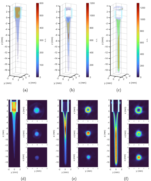
Figure 4. Tomographic reconstructions showing the spatial structure of the APPJ in ambient air using a long camera gate width of 300 ns, integrating the temporal dynamics. Isosurface plots are shown in (a) at 706.5 nm (Hem
), in (b) at 391.4 nm (N (B)), and in (c) at 337.1 nm (N2(C)). Slices along the yz plane at x = 0 mm and along xy planes at
  , and −10 mm (top to bottom) are shown in (d) at 706.5 nm (Hem
), in (e) at 391.4 nm (N
, and −10 mm (top to bottom) are shown in (d) at 706.5 nm (Hem
), in (e) at 391.4 nm (N (B)), and in (f) at 337.1 nm (N2(C)). The quartz tube position and size are marked with light blue rectangles. Colorbars in (a), (b), and (c) correspond to (d), (e), and (f), respectively.
Download figure:
Standard image High-resolution image
Figure 5. Isosurface plots at 706.5 nm (Hem ) from tomographic reconstructions using a camera gate width of 5 ns to resolve temporal dynamics. The time points correspond to 60, 100, 130, 180, and 240 ns (left to right) after the start of the high voltage pulse.
Download figure:
Standard image High-resolution image
Figure 6. Isosurface plots at 391.4 nm (N (B)) from tomographic reconstructions using a camera gate width of 5 ns to resolve temporal dynamics. The time points correspond to 60, 100, 130, 180, and 240 ns (left to right) after the start of the high voltage pulse.
Download figure:
Standard image High-resolution image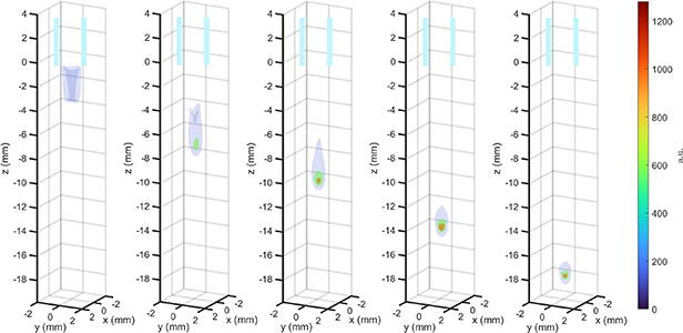
Figure 7. Isosurface plots at 337.1 nm (N2(C)) from tomographic reconstructions using a camera gate width of 5 ns to resolve temporal dynamics. The time points correspond to 60, 100, 130, 180, and 240 ns (left to right) after the start of the high voltage pulse.
Download figure:
Standard image High-resolution imageThe species considered in figures 4, 5, 6, and 7 are populated and depleted through various mechanisms. Hem
(33S) is populated primarily through electron impact excitation and is depleted through electron impact excitation to higher levels, spontaneous emission (33S to 23P,  s−1 [59]), collisions with N2, O2, H2O, and He atoms [60, 61], and three-body collision reactions with H2O and He molecules [62]. Penning ionization of N2 and O2 is a key process in helium APPJs and leads to fast decreases in emission at 706.5 nm on the timescale of the discharge [63], as can be seen in figure 5. N
 (B) is produced primarily by Penning ionization (Hem
+ N2
(B) is produced primarily by Penning ionization (Hem
+ N2
 N
N (B
(B ) + He,
  cm3s−1) [60]. It is also produced by electron impact ionization and charge transfer reactions with helium dimer ions (He
 + N2
+ N2
 N
N (B
(B ) + 2He,
  cm3s−1) [60]. N
 (B) is depleted through spontaneous emission (B
 to X
to X ,
,  s−1 [64]), electron dissociative recombination (k
=
2
×
10−7 cm3s−1) [65], and deactivated by N2 and O2 (
s−1 [64]), electron dissociative recombination (k
=
2
×
10−7 cm3s−1) [65], and deactivated by N2 and O2 ( cm3s−1 and
  cm3s−1 [66]). The rotational temperature of N
 (B) depends on how the ion is created, and is expected to be near to room temperature [63]. Considering figures 6 and 7, the slower decrease in emission at 391.4 nm in the region from z = 0 to about −9 mm compared to the region from
  to about −18 mm is consistent with a lower density of N2 and O2 diffused into that region.
The excitation of N2 to N2(C) is by electron impact and metastable pooling reactions (N2(A + N2(A
 N2(C
N2(C ) + N2(X
 ),
),  cm3s−1) [67, 68]. The lifetime of N2(A
 in the guided streamer is about 5 µs [69]. Depletion of N2(C) is by spontaneous emission (C
 to B
to B ,
,  s−1 [64]), and quenching by He, N2, and O2 (
 cm3s−1,
  cm3s−1, and
  cm3s−1 [63]). The higher spontaneous emission rate and quenching by He, N2, and O2 lead to decreases in emission at 337.1 nm that are faster than 391.4 nm. The high 337.1 nm light emission at
  mm is consistent with electron densities above 1011 cm−3 predicted by simulation [50].
4.2. APPJ incident on planar dielectric surfaces
Figures 8, 9, and 10 show tomographic reconstructions of the APPJ incident on the planar dielectric surface using an ICCD gate width of 5 ns to resolve temporal dynamics. In figure 8, isosurface plots of constant values designated by the colorbars convey 3D information at 337.1 nm. In figure 9, yz slices from the tomographic reconstructions are shown for plasma light emission at 706.5 nm, 391.4 nm, and 337.1 nm. In figure 10, edge contours drawn from figure 9 highlight difference in plasma light emission at different time points. Figures 8(a) and (b) and the top two rows of figure 9 correspond to time points before and after the IW contacts the surface. The surface was placed 3.3 mm below the quartz tube, or in the region where the Hem
is surrounded by converging regions of N (B) and N2(C), as shown in figure 4. As the IW approaches the surface, charging of the surface creates electric field components parallel to the surface [18], causing the regions or rings of N
 (B) and N2(C) to diverge and then propagate over the surface as part of the SIW. Considering figures 9 and 10, the SIW appears as a layer of Hem
, a layer of N
(B) and N2(C) to diverge and then propagate over the surface as part of the SIW. Considering figures 9 and 10, the SIW appears as a layer of Hem
, a layer of N (B) above the Hem
, and a layer of N2(C) above the N
(B) above the Hem
, and a layer of N2(C) above the N (B) due to mixing with the ambient air.

Figure 8. Tomographic reconstructions showing the temporal evolution of the spatial structure of the APPJ incident on the planar dielectric surface using a camera gate width of 5 ns. Isosurface plots are shown at 337.1 nm (N2(C)). The time points of (a) to (f) correspond to 50, 60, 70, 80, 110, 160 ns after the start of the high voltage pulse.
Download figure:
Standard image High-resolution image
Figure 9. Slices through tomographic reconstructions showing the temporal evolution of the spatial structure of the APPJ incident on the planar dielectric surface using a camera gate width of 5 ns. Slices along the yz plane at constant x = 0 mm are shown in column (a) at 706.5 nm (Hem
), column (b) at 391.4 nm (N (B)) and column (c) at 337.1 nm (N2(C)). The time points correspond to 50, 60, 70, 80, 110, 160 ns (top to bottom) after the start of the high voltage pulse.
Download figure:
Standard image High-resolution image
Figure 10. Edge contours of light emission from Hem
, N (B), and N2(C) drawn from figure 9 (constant x = 0 mm). The time points of (a), (b), and (c) correspond to 60, 80, and 110 ns after the start of the high voltage pulse. Mixing with the ambient air leads to layering of N
 (B) above the Hem
and N2(C) above the N
(B) above the Hem
and N2(C) above the N (B).
(B).
Download figure:
Standard image High-resolution imageIn figure 9(a) corresponding to 50 ns, a high central emission is observed with low emission bulges on either side. The bulges may be created by weak radial components of the electric field caused by the surface leading to space charge induced field enhancement and avalanche in the radial direction. The wavefront of the SIW does not propagate with an orientation parallel to the surface but with a slight vertical angle, likely because the surface ahead of the wavefront is not charged and the fields at the wavefront are not parallel to the surface. This effect can be seen more clearly in figure 9(a) than in figures 9(b) or (c), consistent with the Hem
being closer to the surface, as highlighted in figure 10. As discussed above in section 4.1, a transition from higher electric fields to lower electric fields seems to occur around 100 ns when the emission from N (B) and Hem
decrease while the emission from N2(C) does not. The charging of the surface weakens the SIW as it propagates [17], causing the plasma light emission to decrease and eventually the SIW is extinguished. Figures 8(e) and (f) suggest that the weakening of the SIW is position dependent, leading to non-axisymmetric distributions of the plasma light emission at later times. This may be caused by gas flow, small differences in electrical material properties, or localized non-uniform areas on the surface. The radial speed of the SIW on the planar surface was calculated as
(B) and Hem
decrease while the emission from N2(C) does not. The charging of the surface weakens the SIW as it propagates [17], causing the plasma light emission to decrease and eventually the SIW is extinguished. Figures 8(e) and (f) suggest that the weakening of the SIW is position dependent, leading to non-axisymmetric distributions of the plasma light emission at later times. This may be caused by gas flow, small differences in electrical material properties, or localized non-uniform areas on the surface. The radial speed of the SIW on the planar surface was calculated as  m s−1.
4.3. APPJ incident on structured dielectric surfaces
Figures 11, 12, and 13 show tomographic reconstructions of the APPJ incident on the structured dielectric surface using an ICCD gate width of 5 ns to resolve temporal dynamics. In figure 11, isosurface plots of constant values designated by the colorbar convey 3D morphology at 337.1 nm. In figure 12, xy slices of the tomographic reconstructions through the SIW are shown. In figure 13, slices along planes perpendicular to the trenches are shown to highlight variations along the z dimension and the effects of gas mixing. The trenches are oriented nearly parallel to the y-axis, as shown by the dashed white lines in figure 13, and were large enough for plasma to enter the trench (150 µm, much greater than the expected Debye length [24]). Using conservative estimates of the electron density and temperature in the SIW (1013 cm−3 and 3.5 eV [50, 70]), the Debye length is expected to be 4.4 um, or 34 times smaller than the size of the trench. The spatial resolution of each tomographic reconstruction was 7.4 µm, sufficient to see effects of the structured surface on the SIW. As multiple view angles are required for tomographic reconstruction, the plasma within the trenches could not be reconstructed because of the side-on view of the ICCD shown in figure 1. Therefore, the structure of the plasma just above the surface was investigated tomographically.

Figure 11. Tomographic reconstructions showing the temporal evolution of the spatial structure of the APPJ incident on the structured dielectric surface using a camera gate width of 5 ns. Isosurface plots are shown at 337.1 nm (N2(C)). The time points of (a) to (f) correspond to 50, 60, 70, 80, 110, 160 ns after the start of the high voltage pulse.
Download figure:
Standard image High-resolution image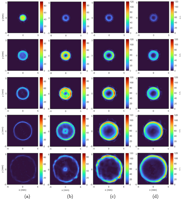
Figure 12. Tomographic reconstructions showing the temporal evolution of the spatial structure of the APPJ incident on the dielectric surfaces using a camera gate width of 5 ns. Slices along the xy plane at constant  mm are shown for the structured dielectric surface in column (a) at 706.5 nm (Hem
), column (b) at 391.4 nm (N
mm are shown for the structured dielectric surface in column (a) at 706.5 nm (Hem
), column (b) at 391.4 nm (N (B)) and column (c) at 337.1 nm (N2(C)). For comparison, slices along the xy plane at constant
  mm are shown for the planar dielectric surface in column (d) at 337.1 nm (N2(C)). Differences between columns (c) and (d) reveal effects of the structured surface. The time points correspond to 60, 70, 80, 110, 160 ns (top to bottom) after the start of the high voltage pulse.
Download figure:
Standard image High-resolution image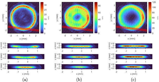
Figure 13. Tomographic reconstructions 80 ns after the start of the high voltage pulse showing the spatial structure of the SIW on the structured dielectric surface using a camera gate width of 5 ns. White dashed lines designate the location of the trenches. Slices along the xy plane at constant  mm and slices along the planes perpendicular to the trenches designated by the red lines are shown in column (a) at 706.5 nm (Hem
), column (b) at 391.4 nm (N
mm and slices along the planes perpendicular to the trenches designated by the red lines are shown in column (a) at 706.5 nm (Hem
), column (b) at 391.4 nm (N (B)) and column (c) at 337.1 nm (N2(C)). The red lines from top to bottom correspond to the slices from top to bottom. Mixing with the ambient air leads to layering of N
 (B) above the Hem
and N2(C) above the N
(B) above the Hem
and N2(C) above the N (B) consistent with figure 10(b).
Download figure:
Standard image High-resolution image
Considering first figure 11, the transition of the guided streamer to a SIW is similar to the planar surface case, with charging of the surface causing the regions of N (B) and N2(C) emission to diverge and then propagate over the surface as part of the SIW. Using the reconstructed data, the radial speed of the SIW on the structured surface was calculated as
  m s−1, the same as the planar surface case. While the speed of the SIW could be expected to decrease on structured surfaces, this was not easily seen within the precision of the measurements presented here.
Considering next figure 12, effects of the surface on the plasma light emission are more obvious. Slices are shown through the volume along the xy plane at constant  mm, or 150 µm above the surface (300 µm above the bottom of the trenches). Plasma light emission is shown in column (a) at 706.5 nm (Hem
), column (b) at 391.4 nm (N
mm, or 150 µm above the surface (300 µm above the bottom of the trenches). Plasma light emission is shown in column (a) at 706.5 nm (Hem
), column (b) at 391.4 nm (N (B)) and column (c) at 337.1 nm (N2(C)). For comparison, slices for the planar dielectric surface are shown in column (d) at 337.1 nm. The influence of the surface appears as regions of lower light emission above the trenches. For the case of a positive bias applied to the APPJ, as was done here, the resulting SIW is expected to adhere to the surface, propagating into and out of the trenches [24]. Therefore, the regions of lower light emission above the trenches are likely a geometric effect. Considering figure 12 columns (c) and (d), the transition of the IW to a SIW at early times is similar for the planar and structured surfaces. The differences include the reduced emission in the regions above the trenches and an increase in emission in the regions above the apex of the trenches. The cause of this increase in emission may be due to effects of field enhancement at the corners of the apex of the trenches. At later times, there is a 'crescent moon' shaped asymmetric feature, where higher light emission is seen in the top right of the SIW as compared to the bottom left. A similarly shaped feature can be seen in figure 4(f), suggesting the effect could be due to the APPJ itself.
In figure 12(b), at the 110 and 160 ns time steps, an inner ring of N (B) emission is observed that does not appear in the Hem
or N2(C) emission. The same effect is also observed for the planar surface, as can be seen in figure 9(b). The cause is not immediately clear, but may be due to gas mixing at the surface and the slower quenching rate of N
(B) emission is observed that does not appear in the Hem
or N2(C) emission. The same effect is also observed for the planar surface, as can be seen in figure 9(b). The cause is not immediately clear, but may be due to gas mixing at the surface and the slower quenching rate of N (B) when compared to Hem
and N2(C) as seen in figures 5, 6, and 7. The final time point shown in the bottom row of figures 12(c) and (d) suggests that the weakening of the SIW due to charging of the surface occurs differently for the structured surface than the planar surface. This can also be seen by comparing figures 11 and 8. This could be due to cumulative effects of variable local surface capacitance or field enhancements at the apex of the trenches, as the gas flow is the same in each case.
(B) when compared to Hem
and N2(C) as seen in figures 5, 6, and 7. The final time point shown in the bottom row of figures 12(c) and (d) suggests that the weakening of the SIW due to charging of the surface occurs differently for the structured surface than the planar surface. This can also be seen by comparing figures 11 and 8. This could be due to cumulative effects of variable local surface capacitance or field enhancements at the apex of the trenches, as the gas flow is the same in each case.
In figure 13, slices through the SIW at 80 ns after the start of the high voltage pulse are shown in column (a) at 706.5 nm (Hem
), column (b) at 391.4 nm (N (B)) and column (c) at 337.1 nm (N2(C)). Slices along the xy plane at constant
  mm are shown again with white dashed lines added that designate the locations of the trenches. Slices along planes perpendicular to the trenches are also shown to convey structure in the z dimension. The position of these planes is designated by the three red lines, which correspond from top to bottom with the lower figures. The effects of mixing with the ambient air at the wavefront of the SIW can be seen, including layering of N
 (B) above the Hem
and N2(C) above the N
(B) above the Hem
and N2(C) above the N (B), consistent with figure 10(b) and the flat surface. As discussed above, the wavefront propagates with a slight vertical angle, likely due to charging of the surface ahead of the SIW. Considering figures 1(c) and 3(a), figures 12 and 13 demonstrate the ability of tomographic reconstructions to recover complex spatial structure in the plane perpendicular to the camera fields of view.
5. Conclusion
Many plasma types and behaviors such as IWs, SIWs, streamers, arcs, cathode spots, anode spots, and magnetic field interactions, and the associated instabilities, create non-symmetric, fully 3D plasma structures. Laser diagnostics and models can investigate well-controlled idealized plasmas in 2D fashion but understanding the complex structure in non-symmetric plasmas can benefit from tomographic imaging techniques that provide a more complete 3D picture.
At atmospheric pressure, plasma distribution is heavily influenced by surfaces and the coupling interactions between plasma properties and the interfacing material properties. Here, Tomo-OES was used to investigate an APPJ and SIWs on planar and structured surfaces. The results demonstrate that Tomo-OES is suitable for characterization of IWs and SIWs with acceptable temporal and spatial resolution. Only simple dielectric surface structures were considered, but 3D printing offers a convenient method for fabricating more complex structures and structure distributions that influence propagation of SIWs, such as wavy surfaces, cones, cylinders, pores, etc that may exhibit useful collective effects.
Tomography is useful for 3D model validation and solves the line-of-sight integration problem in optical diagnostics, allowing recovery of localized spectroscopic information. Future work could investigate interactions of multiple SIWs and determine plasma parameters using the line-ratio method [58]. Single-shot measurements are possible using multiple cameras. In principle the approach could be adapted to account for surface reflections and light transport through media like liquid water and tissue, allowing tomographic reconstructions within these media.
Acknowledgments
The author thanks Kevin Youngman and Richard K Harrison at Sandia National Laboratories and Peter Bruggeman at the University of Minnesota for productive conversations, laboratory equipment support, and the APPJ. This work was supported by the U.S. Department of Energy, Office of Science, Office of Fusion Energy Sciences under Award Number DE-SC0020232. This work was also supported by the Laboratory Directed Research and Development (LDRD) Program at Sandia National Laboratories. Sandia National Laboratories is managed and operated by National Technology & Engineering Solutions of Sandia, LLC, a wholly owned subsidiary of Honeywell International Inc. for the U.S. Department of Energy's National Nuclear Security Administration under Contract DE-NA0003525.
Data availability statement
All data that support the findings of this study are included within the article (and any supplementary files).
Conflict of interest
The author has no conflicts of interest to disclose.