
Abstract
Large-area epitaxial growth of III–V nanowires and thin films on van der Waals substrates is key to developing flexible optoelectronic devices. In our study, large-area InAs nanowires and planar structures are grown on hexagonal boron nitride templates using metal organic chemical vapor deposition method without any catalyst or pre-treatments. The effect of basic growth parameters on nanowire yield and thin film morphology is investigated. Under optimised growth conditions, a high nanowire density of 2.1  109 cm−2 is achieved. A novel growth strategy to achieve uniform InAs thin film on h-BN/SiO2/Si substrate is introduced. The approach involves controlling the growth process to suppress the nucleation and growth of InAs nanowires, while promoting the radial growth of nano-islands formed on the h-BN surface. A uniform polycrystalline InAs thin film is thus obtained over a large area with a dominant zinc-blende phase. The film exhibits near-band-edge emission at room temperature and a relatively high Hall mobility of 399 cm−2/(Vs). This work suggests a promising path for the direct growth of large-area, low-temperature III–V thin films on van der Waals substrates.
Export citation and abstract BibTeX RIS

Original content from this work may be used under the terms of the Creative Commons Attribution 4.0 licence. Any further distribution of this work must maintain attribution to the author(s) and the title of the work, journal citation and DOI.
1. Introduction
III–V compound semiconductor materials are of great importance in various applications such as light emitting diodes (LEDs) [1], lasers [2–4], sensors [5] and solar cells [6]. Recent years have seen a growing research interest in low-temperature-grown semiconducting materials for various applications such as sensors integrated above integrated circuits (IC), display technologies and back-end-of-line integration [7, 8]. Low-temperature (<500 °C) processing is indeed crucial for these applications as the substrate or the deposited layers involved might not be compatible with high-temperature processes. Incorporating low-temperature-grown semiconductor materials on cheap and flexible substrates has the further merit of reducing production costs.
Epitaxial growth of III–V nanowires (NWs) and thin films (TFs) have been explored extensively on conventional substrates such as GaAs and Si. For NW growth, a well-explored growth mechanism is the vapor–liquid–solid (VLS) mechanism. However, using gold as a catalyst raises concerns of its incorporation in the grown material. This issue has been addressed by alternative growth methods such as self-catalyzed and catalyst-free growth on various types of substrates.
The growth of III–V TFs has been mostly investigated on lattice-matched substrates. When grown on substrates of dissimilar lattice parameter (e.g. Si), buffer layers have been employed to accommodate the strain due to lattice and thermal mismatch. Such heteroepitaxial growth of III–Vs on Si or dielectric SiO2/Si substrates has also been explored and shown promising results [9]. However, high-quality heteroepitaxy remains challenging to achieve. The deposited material often shows nano or micro-scale grain sizes and little morphology control given the large lattice and thermal mismatch.
Over the past decade, interest in III–V compound semiconductor NW and TF growth on unconventional and novel substrates such as van der Waals (vdW) or two-dimensional (2D) substrates has grown. The use of various vdW substrates such as synthetic mica [10], graphene [11, 12], h-BN [13] and MoS2 [14], with metal–organic chemical vapor deposition (MOCVD), molecular beam epitaxy (MBE) and chemical vapor deposition (CVD) has been reported. III–V TF growth on 2D substrates, although very attractive for the obvious reasons of relaxing the strict requirement of lattice and thermal matching, has been largely unexplored.
With the rise of vdW epitaxy research in recent years, monolayers of 2D materials, such as graphene, are being utilized as an epitaxial template for uniform TF growth, creating an opportunity for integrating III–V semiconductors on Si [12]. Research in this area often focuses on using 2D materials that are exfoliated mechanically, which presents scalability issues. This can be alleviated if III–V semiconductors are grown on large-area vdW substrates, such as synthetic mica, or wafer-scale 2D materials. Moreover, the wealth of information available about NW growth mechanism, including position control, dimensions, crystal structure, NW quantum wells and quantum dots, can be emulated in vdW epitaxy. Much progress has been achieved in recent years in the growth of III–V NWs on graphene. A recent review article on vdW epitaxy of III–V NWs gives an account of various methods used to achieve NW and device structures [15]. However, more research and development is required to explore the most suitable 2D substrates and growth conditions for potential commercial-scale heteroepitaxy and device applications.
Hexagonal boron nitride (h-BN) is a 2D-layered material very similar to graphene in terms of crystal structure and lattice parameter. The significant difference lies in their physical properties, such as band structure, optical and electrical characteristics [16]. Highly crystalline quality III-nitrides can be grown on h-BN [17]. The unique layered structure of vdW substrates allows the peel-off of as-grown micro- and nanostructures and TFs.
Despite the growing interest in this field, only a few reports on the growth of III–V NWs and TFs on 2D material substrates are available. This study reports on large-area catalyst-free growth of InAs NWs and TFs on few-layer h-BN transferred on to SiO2/Si substrate. h-BN on SiO2/Si substrate was purchased from Grolltex Inc. USA, figure S1 in supporting information provides more details about the h-BN layer properties. By systematically studying various growth conditions, it is shown that a high yield of vertically oriented NWs and uniform TF growth are possible on the h-BN surface. This work lays the foundation for further research toward achieving high-density III–V NWs and single crystalline III–V TFs on 2D materials.
2. Experimental methods
Catalyst-free InAs NW and TF growth on large-area few-layer h-BN on SiO2/Si substrates was conducted in a horizontal-flow MOCVD reactor using trimethylindium (TMIn) and arsine (AsH3) as the group III and group V precursors, respectively, with hydrogen as the carrier gas. The MOCVD reactor was first pumped down to a pressure of 100 mbar. InAs NWs and TFs were grown using a single-temperature growth step. The reactor was heated to the desired growth temperature (TG) in a hydrogen atmosphere before TMIn and AsH3 were introduced to initiate growth. NW growth was carried out for 15 min, after which the reactor was allowed to cooled under ambient AsH3 until the temperature dropped below 350 °C. The effects of TG (450 °C–600 °C) and V/III ratio (3–40) on NW density, length and diameter were investigated. The V/III ratio for NW growth was varied by keeping the group III flow rate at 6.206 × 10⁻⁶ mol min−1 and changing the group V flow rate correspondingly. The influence of both TG and V/III ratio were also studied for achieving uniform TF growth. Experiments to study the effect of V/III ratio on TF growth were carried out to obtain maximum areal coverage of smooth TF. This was done first by varying the group V flow between 4.464 × 10⁻⁴ and 6.696 × 10⁻³ mol min−1 while keeping the group III flow rate constant at 1.241 × 10⁻⁵ mol min−1 (V/III ratio in the range of 40-540), and then by varying the group III flow rate between 5.820 × 10⁻⁵ and 1.241 × 10⁻⁵ mol min−1 while keeping the group V flow rate constant at 2.500 × 10⁻³ mol min−1 (V/III ratio in the range of 40–200). Morphological and structural characterizations of the NWs and TFs were carried out using scanning electron microscopy (SEM, FEI Verios 460L), atomic force microscopy (Bruker ICON AFM) and transmission electron microscopy (TEM, JEOL JEM-2100F). Optical characterizations were carried out by infrared reflectance and photoluminescence (PL) measurements. Infrared reflectance was performed using a Fourier-transform infrared spectrometer (FTIR, Frontier, Perkin Elmer) coupled with a microscope under ambient environment. A liquid-nitrogen-cooled HgCdTe detector was used with a Cassegrain objective. Measurements were carried out over a 100 × 100 μm2 area using a variable aperture. The spectra were acquired at a resolution of 4 cm−1 and referenced against a reflecting gold surface of the same area. Infrared PL spectra were measured at room temperature using an FTIR (iS50, Thermo Fisher) at an excitation wavelength of 638 nm and a liquid-nitrogen-cooled HgCdTe detector through a 15× objective.
3. Results and discussion
3.1. InAs nanowires on hBN/SiO2/Si
The effects of TG and V/III ratio are studied to achieve NWs with high vertical yield, good morphology and crystal structure.
3.1.1. Effect of growth temperature
The SEM images in figures 1(a)–(d) show NWs grown at various TG and V/III ratio of 10. At a low TG of 450 °C, nanoislands are predominantly formed. This can be indicative of a low adatom diffusion length on the h-BN surface at the given TG. As the temperature is increased further, NWs grow in considerable density with the highest density being 2.1  109 cm−2 at 500 °C, which is an order of magnitude higher than what is reported for InAs NWs grown on graphitic substrates using a self-catalyzed growth strategy [18]. The NW density then reduces as TG is increased further to 600 °C. The morphologies of the NWs also evolves as a function of TG. The plots of the length, diameter and NW density as a function of TG are shown in figures 1(e) and (f). Here, we observe that the NWs length is directly proportional and the diameter inversely proportional to TG. The observed morphology evolution is expected due to the competition between axial and radial growth. With increasing TG, the axial growth rate is enhanced at the expense of the radial growth rate, due to the enhanced adatom diffusion length allowing migration to the top of the NWs. This is further evident from the non-tapered NW morphology. Therefore, longer NWs with smaller diameters are observed with increasing TG.

Figure 1. SEM images of InAs NWs grown on hBN/SiO2/Si at different growth temperatures: (a) 450 °C, (b) 500 °C, (c) 550 °C, and (d) 600 °C. All scale bars indicate 1 μm. (e) Distribution of NW length (red) and diameter (blue) as a function of growth temperature. (f) Density of NWs as a function of growth temperature.
Download figure:
Standard image High-resolution imageThe observed NW density variation is due to the same phenomenon. At higher TG, the high mobility of the adatoms results in fewer adatoms able to spontaneously nucleate to form NWs, hence the observed reduction in NW density at high TG. Furthermore, the vertical orientation of InAs NWs on h-BN is indicative of a good epitaxial relationship between them. This is similar to what has been reported for InAs NWs grown on graphene, where the authors concluded that, the epitaxial relationship is due to near-lattice-matching conditions between the InAs NWs and graphene [18, 19].
3.1.2. Effect of V/III ratio
The effect of V/III ratio on the morphology of NWs at a constant TG of 500 °C is shown in the SEM images of figures 2(a)–(d), which corresponds to V/III ratios of 3, 5.4, 10 and 40, respectively. Plots of the NW density, length and diameter as a function of V/III ratio are shown in figures 2(e) and (f). The density of the NWs increases with V/III ratio from 3 to 5 but decreases significantly afterwards. At a low V/III ratio, there is less AsH3 in the growth environment and hence less nucleation, leading to an overall decrease in the number of NWs. On the other hand, at a high V/III ratio, the mobility of In adatoms is reduced and more spontaneous nucleation occurs on the h-BN surface, which results in the coalescence of these nuclei rather than the formation of NWs, thereby leading to a reduction in NW density. The activation energy for the heterogeneous reaction at the growth interface decreases as the V/III ratio is increased. The observed reduction in NW length and the considerable increase in NW diameter with V/III ratio is attributed to the radial growth competing with axial growth. Once again, this stems from the reduced In adatom mobility at higher V/III ratios, leading to a more prominent deposition on the NW side-walls than at its tip. This results in the NW coalescence and nanoislands are inevitably formed on the h-BN surface during growth, as observed in figure 2(d). A further increase in V/III ratio can lead to the formation of an InAs TF on h-BN. Uniform TF growth is explored later in this work.
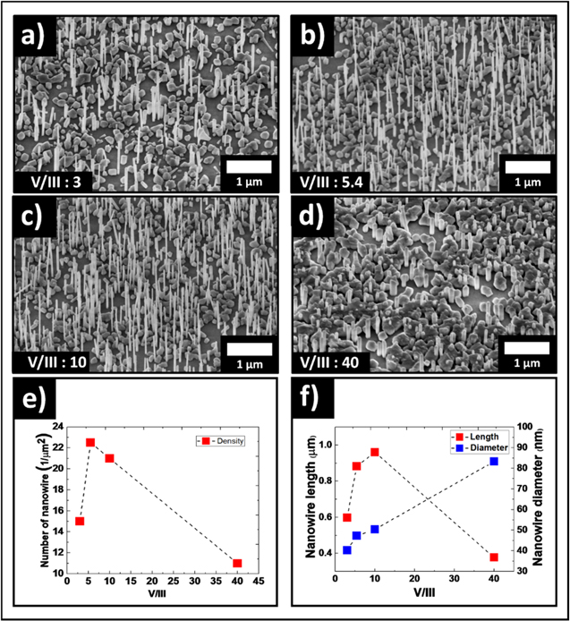
Figure 2. SEM images of InAs NWs grown on a hBN/SiO2/Si with different V/III ratios: (a) 3 , (b) 5.4, (c) 10, and (d) 40. All scale bars indicate 1 μm. (e) NW density as a function of V/III ratio. (f) Distribution of NW length and diameter as a function of V/III ratio).
Download figure:
Standard image High-resolution imageA TEM investigation of the NWs shows that they are all formed in a mixed zinc- blende/wurtzite (ZB/WZ) phase with no specific dependence on the growth temperature or V/III ratio (supporting information—figure S2).
3.2. InAs TF on hBN/SiO2/Si
The epitaxy of III–Vs on 2D material templates usually involves the modification of the vdW surface by etching techniques to promote nucleation sites. A review on recent developments in vdW epitaxy of III–V semiconductors on 2D materials reports the various surface treatments carried out to promote and control the growth [15]. These treatments, however, deteriorate the surface and affect its physical properties. One of the first attempts to grow a continuous TF of GaAs on graphene was reported by Alaskar et al [12]. using MBE on mechanically exfoliated multilayer graphene layers transferred on SiO2/Si substrates. They conclude that the high surface tension, caused by the low surface energy of 2D materials and the low adsorption and migration energy of Ga, In, Al, As species on the graphitic surface, is the principal obstacle to achieve 2D growth of III-As materials on graphene.
In this section, we explore how we can utilize the formation of nanoislands described above (figures 1 and 2) to grow a uniform InAs TF on h-BN/SiO2/Si by systematically studying the growth parameters. TG is kept constant to study the effect of the V/III ratio on the nanoislands formation and coalescence. As shown by the schematic in figure 3(a), by increasing the V/III ratio, the NWs aspect ratio is reduced considerably and they start to coalesce into nanoislands. As shown in the SEM images in figures 3(b)–(d), increasing the V/III ratio beyond 40 inhibits of NW formation whilst simultaneously increasing the size of the nanoislands. Results on the effect of growth conditions as presented in supporting information figure S3 show that an optimum V/III ratio of 200 and TG of 475 °C can achieve a uniformely covered TF. Here, the group III flow rate was kept constant while the group V flow rate was varied, to maintain the same growth rate across experiments. Dayeh et al [20] demonstrated that the temperature profile of NW growth is strongly influenced by the input V/III ratio. Because a high V/III ratio lowers the activation energy for planar growth and reduces the adatom diffusion length. Hence, it can be concluded that at low TG and at relatively high V/III ratio, the In adatom mobility is reduced causing crystallisation on the hBN substrate surface rather than on the NW growth site.
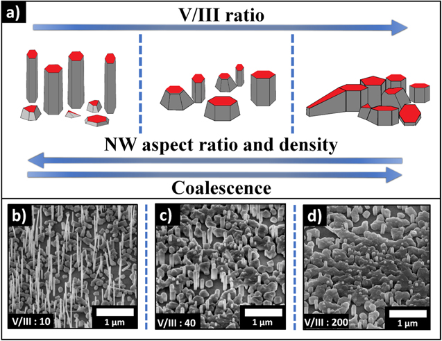
Figure 3. (a) Schematic of the conditions for the suppression of NW axial growth and the coalescence of nanoislands. (b)–(d) 45°-tilted SEM images showing the morphology of NWs and nanoislands at different V/III ratios.
Download figure:
Standard image High-resolution imageFigures 4(a)–(c) depict the TF growth at V/III ratios of 74, 100 and 200, respectively. These ratios were achieved by changing the group III flow rate while maintaining a fixed group V flow rate of 2.5 × 10⁻³ mol min−1. The growth temperature was set at 475 °C and the growth times were adjusted to compensate for the growth rate variation, with the goal that all samples have the same total amount of group III precursor deposited (3.723 × 10⁻⁵ mol). The growth times (indicated in figures 4(a)–(c)) are adjusted to compensate for the growth rate variation, as a result of varying the group III flow rate.
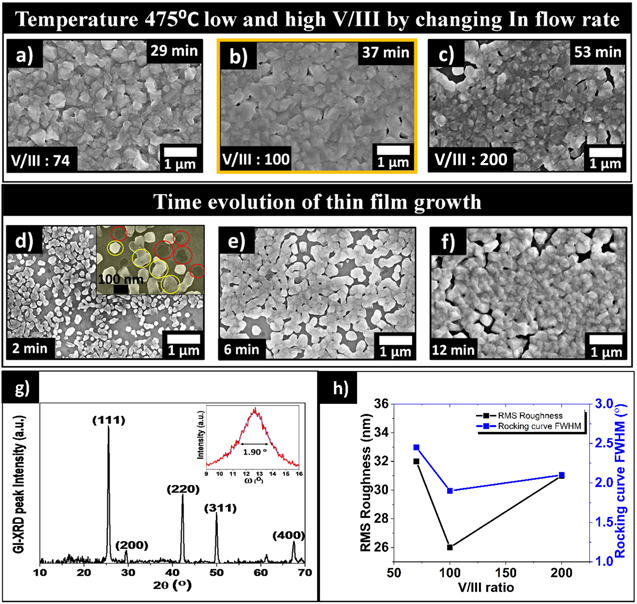
Figure 4. Top-view SEM images of the InAs TFs grown at V/III ratios of 74 (a), 100 (b) and 200 (c). Top-view SEM images showing the time evolution study of the TFs grown at 475 °C with a V/III ratio of 100 for 2 (d), 6 (e), and 12 (f) min. The inset in (d) shows a magnified image of the 2 min sample, clearly showing 2D platelets (layer-by-layer growth) encircled in red and nano island encircled in yellow nucleation happening simultaneously. The GIXRD spectrum of the sample shown in (a) is shown in (g), with the inset showing the rocking curve of the (111) peak. AFM RMS surface roughness and rocking curve FWHM obtained from TF grown at V/III ratios of 74, 100 and 200 at a growth temperature of 475 °C are shown in figure (h).
Download figure:
Standard image High-resolution imageThe growths resulted in a uniform coverage of polycrystalline TF with smooth morphology, as shown in figures 4(a)–(c). At a V/III ratio of 100, the TF exhibits a smooth morphology (figure 4(b)) with relatively low RMS surface roughness and narrow rocking curve full-width-at-half-maximum (FWHM), compared to TFs grown at other V/III ratios as shown in figure 4(h). Thus, the observed growth window of low temperature (475 °C) and high V/III ratio (100) shown in figure 4(b) is ideal for TF growth on h-BN surface through a catalyst-free vapor-solid growth mode.
A time evolution study of the best morphology obtained is carried out to analyse the TF growth mode on the hBN surface. Figures 4(d)–(f) show the time evolution study with 2, 6 and 12 min growth durations, respectively. The SEM analysis of the 2 min growth sample (inset shows a magnified view), shows that 2D hexagonal platelets and islands are formed simultaneously. Thus of Volmer–Weber (island growth) and Stranski–Krastanov (SK) growth modes occur simultaneously.. Ideally, to obtain a uniform TF with smooth morphology, a layer-by-layer growth mode is required. Although layer-by-layer nucleation can happen locally on a vdW surface, lateral growth becomes challenging above a certain nucleus size, due to the low surface energy and high surface tension properties of the underlying hBN.
As growth progresses, the SK growth mode competes over the island growth mode as evidenced by figures 4(d)–(f), where the nanoisland structures coalesce with 2D platelet structures and other nanoislands.
3.2.1. Crystal structure and strain properties of the thin films
The cross-sectional TEM image of a focussed ion beam (FIB)-cut TEM lamella of the best morphology TF (grown at TG 475 ℃ and V/III ratio of 100) is shown in figure 5(a). The TF has an average grain size of approximately 0.45 μm. Figures 5(b) and (c) show the high resolution TEM (HRTEM) images of the areas marked by coloured boxes in 5 (a). The ZB and WZ/twin areas are highlighted in green and red, respectively. The TF exhibits a predominantly a ZB crystal structure with rotational twin defects and WZ/twin defects in the grain boundaries as evident from figure 5(b). Bulk InAs exists naturally in the ZB crystal phase.
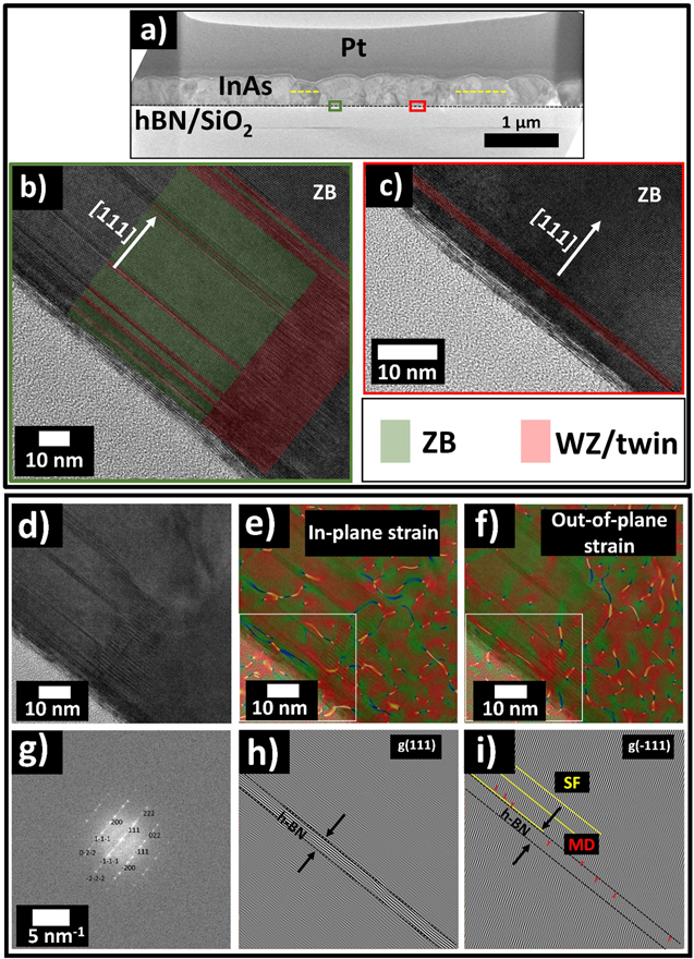
Figure 5. (a) FIB-cut TEM lamella of the polycrystalline InAs thin film grown on h-BN/SiO2/Si substrate. (b)–(c) HRTEM images of InAs/hBN interface from the green and red areas on figure (a), showing ZB and WZ/twin sections, respectively. (d) HRTEM image for GPA strain analysis the colour variation represents the difference in the magnitude of strain with red and green corresponding to the maximum and minimum strain areas. (e) In-plane strain map (f) Out-of-plane strain map overlaid on the HRTEM image. (g) Fast Fourier transform of the HRTEM image in (d). Fast Fourier transform of g(1 1 1) (h) and g(−111) (i).
Download figure:
Standard image High-resolution imageFigure 5(d) shows a HRTEM image of InAs grown on h-BN, captured along the [0 –11] zone axis, The image is used to carry out the geometric phase analysis (GPA) to study the local strain at the TF and h-BN interface. The two non-parallel directions of [111] and [−111] are chosen for the GPA. The in-plane and out-of-plane strain analysis along [111] and [−111] directions, respectively shown in figures 5(e) and (f), do not indicate a sharp interfacial strain between h-BN and InAs. Figure 5(g) shows the fast Fourier transform (FFT) of the HRTEM image of figure 5(d). From the FFT, the direction of InAs TF growth is deduced to be along [111].
To further understand the h-BN/InAs interface and the lack of a sharp interfacial strain in GPA (the colour variation figures 5(e) and (f) represents the difference in the magnitude of strain), we analysed the inverse fast Fourier transform (IFFT) of the HRTEM images shown in figures 5(h) and (i). IFFT analyses were carried out using the (111) and (−111) diffraction spots (figure 5(g)). Although the out-of-plane results along the [111] growth direction show the presence of some dislocations within the InAs layer near the h-BN/InAs interface, dislocations are not observed at the h-BN/InAs interface itself. However, IFFT results of out-of-plane g(−111) show the presence of misfit dislocations (marked as MD in red) near the interface, as shown in figure 5(i). Furthermore, stacking faults (marked as SF) commonly present in face-centered cubic crystals on {111} planes due to easy slip have been observed and are indicated with a yellow line in figure 5(i). The fact that stacking faults are present near the interface and away from the interface leads us to conclude that they result from non-optimal growth rather than originating from the h-BN/InAs interface. Finally, the absence of a sharp interfacial strain in InAs grown on h-BN is attributed to the presence of misfit dislocations at the h-BN/InAs interface, which act as an efficient strain relaxation mechanism.
Threading dislocations are generally caused by strain induced in the TF when grown on a lattice-mismatched substrate. Although h-BN and InAs are not lattice-matched, strain-induced dislocations are not expected when grown directly on a vdW substrate owing to the weak vdW nature of bonding at the InAs/h-BN interface as opposed to the strong covalent bonding when grown on conventional bulk substrates. In our previous work on the growth of vertically-oriented GaAs NWs on synthetic mica, a 2D-layered material, DFT calculations showed there is negligible charge transfer across the GaAs/mica interface [10]. The calculated lowest energy configuration showed that the GaAs/mica interface has a physisorption-type bonding rather than covalent, owing to the vdW nature. Hence, as expected in vdW epitaxy, threading dislocations are absent in the InAs TF grown on h-BN surface.
3.2.2. Optical and electrical properties of thin film
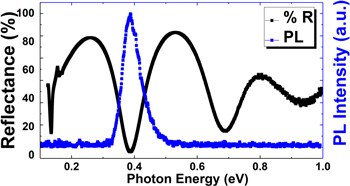
Results from room temperature PL and reflectance measurements of the TF sample grown under optimal conditions (TG 475 °C and V/III ratio 100) are shown in figure 6. The sample exhibits a PL emission peak at 0.39 eV with a FWHM of 69 meV. The reflectance spectrum also exhibits an absorption peak centered at 0.39 eV. Furthermore, the reflectance is over 80% can be observed at other wavelengths, which is consistent with a relatively smooth surface morphology of the TF. Note that the PL emission peak is near the band edge emission of bulk (ZB) InAs (bandgap Eg = 0.36 eV). The blueshift (∼30 meV) in PL emission peak compared to the bandgap energy of InAs can be attributed primarily to the strain introduced in the epilayer while cooling down after growth. In heteroepitaxial growth, a biaxial strain is induced between two materials due to their lattice parameter difference. When the TF is grown over the critical thickness, the biaxial strain is relieved by misfit dislocations. This can result in unstrained, bulk-like material beyond the region of misfit dislocations. The misfit dislocations from the GPA discussed earlier supports this observation. However, during the cool down step from TG, biaxial strain in the TF can be induced again, due to the significant difference between the coefficient of thermal expansion of the epilayer and the substrate.
Figure 6. Room temperature PL (blue) and reflectance spectra (black) of InAs TF grown on hBN surface.
Download figure:
Standard image High-resolution image
We propose that the significant difference in linear thermal expansion coefficients between InAs (4.52 × 10⁻⁶ °C−1) and h-BN [21] (−3.58 × 10⁻⁶ °C−1; negative values in the direction perpendicular to the plane) results in a biaxial strain in the InAs layer, leading to a PL blueshift of ∼30 meV. The electrical properties of the polycrystalline InAs TF was determined using a van der Pauw Hall measurement system at room temperature. The TF shows an n-type behaviour with a resistivity of 1.621 × 10⁻⁴ ohm cm, a Hall mobility of 399 cm2/(Vs) and a carrier density of 9.510 × 1019 cm−3. While pure InAs bulk material exhibits very high room temperature carrier mobility (44000 cm2/(Vs)), polycrystalline III–V TFs reported in the literature exhibit carrier mobilities in the range of 100–150 cm2/(Vs) [8]. As per the Matthiesen rule, major factors affecting carrier mobility in a polycrystalline TF sample are phonon scattering, Coulomb interaction and surface roughness [22]. The TF presented in this work has better electrical characteristics compared to those typically grown at low temperatures (<500 °C) on amorphous substrates reported in literature [23]. We attribute this relative superiority to the greater areal coverage, relatively low surface roughness of the as grown thin film compared to other reported InAs thin film structures on unconventional substrates [8] and a higher average grain size of InAs TF grown on hBN surface. Thus, the TF presented in this work serves as an excellent template for subsequent growth of other III–V layers.
4. Conclusion
InAs NWs and TFs are successfully grown on a h-BN/SiO2/Si vdW substrate without employing any catalyst or surface modification techniques. A very high density of NWs (2 × 109 cm−2) is achieved by varying the growth temperature and V/III ratio. The NWs were found to have a mixed WZ/ZB phase across the range of growth parameters studied. A growth strategy to achieve uniform InAs TFs on h-BN/SiO2/Si by supressing the NW growth and increasing the radial growth of the nano-islands nucleated on the h-BN surface is reported. The growth parameters such as temperature and V/III ratio, with detail surface morphology, structural and optical properties are investigated. The structural properties of the InAs TF are mostly affected by the temperature and not the V/III ratio. Cross-sectional TEM, which is supported by the XRD and GPA results, reveals a largely [111] oriented ZB structure. The blueshift in PL is attributed to the biaxial strain induced by the difference in thermal expansion coefficient between h-BN and InAs TF. The vdW nature of the interface is further evident from the lack of threading dislocations extending to the top of the film. The uniform coverage of the polycrystalline InAs TF combined with its room temperature PL and a relatively high Hall mobility of 399 cm2/(Vs) indicate that this technique can be used to achieve large-area, low-temperature growth of III–V TFs directly on van der Waals substrate using MOCVD.
Acknowledgments
We acknowledge the Australian Research Council for financial support. Access to the epitaxial growth and fabrication facilities is made possible through the Australian National Fabrication Facility, ACT Node. N H acknowledges support from the Postdoctoral Fellowships for Research Abroad of Japan Society for the Promotion of Science. Luminescence studies at Berkeley were funded by the US Department of Energy, Office of Science, Office of Basic Energy Sciences, Materials Sciences and Engineering Division under contract DE-AC02-05-CH11231 (EMAT program KC1201). We acknowledge the Australian National University node of Microscopy Australia for access to the transmission electron microscope.
Data availability statement
All data that support the findings of this study are included within the article (and any supplementary files).
Conflict of interest
There are no conflicts of interest to declare.
Supplementary data (1.2 MB PDF)