

Abstract
Piezoelectric materials have drawn significant attention from researchers in the recent past as the piezo-potential, induced by applied external stress, generates an electric field, which paves the way for the creation and transfer of electrons and holes. After the theoretical prediction of the existence of the piezoelectric effect in transition metal dichalcogenides (TMDCs) semiconductors, intense research efforts have been made by various researchers to demonstrate the effect experimentally. In addition 2D TMDCs exhibit layer-dependent tunable electronic structure, strongly bound excitons, enhanced catalytic activity at their edges, and novel spin/pseudospin degrees of freedom. The edge sites and activated basal planes of 2D TMDCs are shown to be highly active toward catalysis of the hydrogen evolution reaction (HER). However, as compared to electrocatalytic or even photocatalytic performances, TMDC materials exhibit poorer piezocatalytic activity, in general. Therefore, a numbers of research strategies have been made to intensify the piezoelectric effect by synthesizing different types of TMDC nanostructures, by coupling the piezoelectric effect with the photocatalytic effect, by doping with other materials, etc. This review discusses various techniques of synthesis of TMDCs nanostructures and the recent progresses in applications of TMDC nanomaterials in piezocatalysis. In the present article, the piezocatalytic dye degradation performances and HER activity using different TMDCs have been reviewed in detail. Different methods of increasing the piezocatalytic activity of various TMDCs nanostructures have been illustrated. Here, it has also been attempted to systematically summarize and provide an outlook of the charge transfer behaviour and catalytic mechanisms in large varieties of TMDC piezocatalysts and piezo-photocatalysts. In addition, advanced applications of TMDC piezocatalytic materials as piezoelectric nanogenerator, piezocatalytic dye degradation, piezo−phototronic dye degradation and HER studies have been highlighted.
Export citation and abstract BibTeX RIS
1. Introduction
Nanoscience in the broader sense is the study of structures and molecules having at least one of its dimensions on the scales of nanometres ranging between 1 and 100 nm. Nanoscience and nanotechnology have opened extensive and expanding research areas, which include structures, instruments, and systems with novel properties [1, 2]. The field of nanotechnology has already gained a lot of social cognizance and it was a topic of debate and controversy in the early twentieth century. This in turn has initiated the commercial applications of nanotechnology. Nanotechnology has a contribution to almost every field of science including chemistry, physics, biology, material science, computer science, and engineering [3–5].
According to Siegel, the nanostructured materials are classified as, zero dimensional (0D), one dimensional (1D), two-dimensional (2D), and three-dimensional (3D) nanomaterials [6, 7]. In case of 0D nanomaterials, including quantum dots (QDs), all dimensions (x, y and z) are at the nanoscale, i.e. no dimensions are greater than the corresponding exciton Bohr radius [6, 7]. In 1D nanomaterial, two dimensions (x, y) are at nanoscale and the other is outside the nanoscale. The list of 1D material includes nanofibres, nanotubes, nanorods, and nanowires. In 2D nanomaterials, one dimension (x) is at the nanoscale and the other two are outside the nanoscale. The 2D nanomaterials exhibit plate-like shapes. The list of 2D material includes nanosheets, nano-films, nano-layers, and nano-coatings with nanometre thickness [8–10]. The 3D nanomaterials are the nanomaterials in which charge carriers are not confined in any nanoscale dimension. The bulk (3D) nanomaterials are composed of multiple arrangements of nanosized crystals in different orientations. It includes nanoparticles dispersions, nanowire, and nanotube bundles as well as multi-nanolayers (polycrystals) in which the 0D, 1D, and 2D structural elements are in close contact with each other and form interfaces which includes spheres, cubes, etc [8–10].
After the discovery of graphene by AK Geim and K Novoselov in 2004, the research on 2D layered materials has gained a huge impetus, and it is a milestone in the research of 'quantum confinement' [10]. Recently, other 2D materials such as transition metal dichalcogenides (TMDCs), hBN, MXene, etc have been highlighted so much due to their effective applications in modern technology [11–14]. The band structure calculations identifying unique changes in bandgap as a function of material dimensionality and layer number in silicene, TMDCs, and phosphorene motivated the rapid expansion of research into 2D materials beyond graphene [15]. In addition to having a layer-dependent and therefore tunable electronic structure, 2D TMDCs exhibit strongly bound excitons, enhanced catalytic activity at their edge states, and novel spin/pseudospin degrees of freedom [15–17]. The edge sites and activated basal planes of 2D TMDCs have been shown to be highly active toward catalysis of the hydrogen evolution reaction (HER) [15–17]. More importantly, the atomically thin TMDCs materials are in the focus due to their direct bandgap nature with strong light–matter interaction as can be thinned down to a few layers [18, 19].
Nowadays, water pollution and its treatment are one of the major research concerns and lots of scientists are trying to find out the remedy for this disastrous problem. Water in the sea and oceans are continuously polluted by different toxic dyes coming from the different textiles, dye, and paint industries and imposes a serious threat to future generation. Wastewater treatment is also a key problem area in present day energy research [20, 21]. Recently, researchers are widely utilizing photocatalysts based on semiconductor nanomaterials to achieve the degradation of organic pollutants by creating strong oxidizing free species under light illumination [22, 23]. So far, various procedures, viz., doping other materials, surface modification and preparation of heterostructured materials, etc have been attempted to improve photocatalytic dye degradation [24]. In any case, these materials and strategies are additionally restricted because of their low solar energy conversion efficiency (<20%), and low light transmission in intensely dyed toxins [25]. In this way, novel climate cordial, recyclable, exceptionally effective strategies and materials are important for approaching wastewater purification procedures.
Mechanical energy is a maintainable abundant normal energy that can be used by utilizing piezoelectric materials [26–31]. Piezoelectric materials can create an electric field in response to an outside mechanical force. An implicit electric field efficiently builds the effective generation and separation of free charge carriers [26–31]. In this way, piezoelectric materials have been generally utilized in piezocatalytic dye degradation [26–33]. As of late, scientists have examined the piezocatalytic properties of a few ordinary piezoelectric semiconductor materials, for example, BaTiO3 [26], BiFeO3 [29], ZnO [25], MoS2 [26–37], MoSe2 [33], and so on. The total colour deterioration can be achieved inside a couple of moments under steady ultrasonic vibration. The TMDC materials have given an excessive consideration in comparison to that of other semiconductor materials as it has been observed that they can degrade the coloured toxic dyes present in waste water only by using mechanical vibration instead of using harmful and costly UV light assisted photocatalytic reaction [30, 31].
The piezoelectric characteristics of a single layer of BN, MoS2, MoSe2, MoTe2, WS2, WSe2, and WTe2 have been first studied theoretically using first principles calculations by Duerloo et al in 2012 [34]. The first successful experimental observation of piezoelectric activity using mechanically exfoliated MoS2 flakes has been reported by Wu et al in 2014 [35]. Since then, a lot of research work has been carried out on the piezocatalytic dye degradation properties of layered TMDC nanostructures [32, 36–41]. By coupling the piezoelectric and catalytic properties together, enhanced catalytic activity in the dark by hydrothermally synthesized MoS2 nanoflowers (NFs) has been demonstrated by Wu et al [36]. Thakur et al [42] studied the piezocatalyst, photocatalyst, and piezophototronic effect of CVD-grown monolayer WS2 on the sapphire substrate. The piezocatalytic degradation of organic pollutants (tetracycline and RhB) by using a few layer TMDC materials (MoS2, WS2, and WSe2) has recently been studied by Li et al [41]. Synthesis of piezocatalytic MoS2 nanoflower (NFs) has been demonstrated by Lin et al [31]. Recently, our group has also reported the ultrafast piezocatalytic degradation of organic dyes by using flower and tube like nanostructures of MoSe2 [38]. The piezoelectric effect of WS2 to improve its HER catalytic performance has been reported by Zhang et al [44]. The free layer-dependent piezoelectricity of O doped MoS2 synthesized by solvothermal method for enhanced piezocatalytic HER from pure water has recently been reported by Lei et al [45].
In this review, the fundamental properties of TMDC semiconductors have been discussed in section 1. In section 2, synthesis processes of different TMDC nanostructures through top-down and bottom-up approaches have been discussed in detail. The origin of the piezocatalytic activity of TMDC nanostructures has been discussed in section 3. In section 4, the piezoelectric performance of some structured TMDCs materials and their applications in piezoelectric nanogenerator (PENG), piezocatalytic degradation of organic pollutants, piezocatalytic HER, etc have been discussed. The dependence of piezocatalytic activity on the effect of different nanostructures along with their size, different synthesis mechanisms, etc has been presented. Details of the proposed piezocatalytic mechanisms presented by various researchers are also discussed in section 4. In section 5, a brief summary of present day applications of various piezocatalytic TMDC materials have been presented. We sincerely believe that this review will draw a lot of attention of the beginners, expert researchers as well as that of industrial researchers of the field to employ 2D TMDCs in different applications in development of piezo-catalytic nanogenerator, piezocatalytic degradation of organic pollutants, and in piezocatalytic hydrogen evolution reactions.
1.1. Fundamentals of TMDC semiconductors nanostructures: properties
The TMDCs materials are composed of a large number of materials and they are known by the chemical formula of MX2, where M signifies the transition metal in the 4–10 groups of the periodic table as highlighted by the purple colour on the periodic table shown in figure 1(a), and X represents the chalcogen components from the group 16 of the periodic table.
Figure 1. (a) Shows the periodic table and position of transition metal and chalcogen element in the periodic table, (b) atomic model of TMDCs in the formula of MX2, (c)–(d) atomic structure of 1T phase and 2H phase MX2.
Download figure:
Standard image High-resolution imageThere are more than 50 known TMDCs, and out of them, approximately two-thirds of the TMDCs show hexagonal lattice and layered structures. The lattice structure is shown in figure 1(b) in which these layered structures are organized by a hexagonal-packed transition metal atom sandwiched between two layers of chalcogen atoms. The transition metal (M) and the chalcogens (X) are bonded by strong intra-layer covalent bonding, and the transition metal (M) has adopted the possible co-ordinations inside the TMDCs as either octahedral (T) or trigonal prismatic (H), as shown in figure 1(c) and figure 1(d), respectively. Generally, bulk TMDCs exist in different stacking orders or polytypes, such as 1T, 3R, and 2H, etc phases. In 2H-MoS2, each Mo atom is prismatically coordinated to six surrounding S atoms, forming a thermodynamically stable phase, whereas, for the metastable 1T-MoS2 phase, six S atoms form a distorted octahedron around one Mo atom. Phase transformation from one to another can be done via intralayer atomic gliding. As an example, 1T-MoS2 can be obtained from 2H-MoS2 by intercalating Li or K. 1T-MoS2 is thermodynamically unstable and hence it slowly converts back to 2H-MoS2 at room temperature. Among the crystal structures, the most stable and effective polytype is the so-called 2H phase. In the 2H phase lattice, two opposite layers of trigonal prismatic MX2 unit cells are attached one after another. Figure 1(d) shows the most common coordination of the basic unit cell of the crystal structures studied in this review.
In bulk TMDCs, the X–M–X layers are weakly bonded by van der Waals force [46]. This weak interlayer bonding helps to cleavage bulk TMDCs into a few-layer or single-layer nanosheet [47]. The weak interlayer bonds lead to easy intercalation of metal atoms or organic molecules between the layers and hence change the physical properties of the host compound [48, 49]. The bulk TMDCs have been widely used due to their change of electronic properties from insulating (e.g. HfS2 [50]) to semi metallic (TiSe2, MoTe2, and WTe2) through semiconducting (2H phase of MoS2, WS2, MoSe2, etc) materials [51]. However, the 2H phase of bulk TMDCs is an indirect bandgap semiconductor, and the enhanced electronic properties observed in TMDCs occur from the d-orbital filling and electronic character of TMDCs [52]. The different electronic structure exhibited by the TMDCs family is associated with the number of valence electrons of the transition metal and its coordination environment [50].
The bulk TMDCs are indirect bandgap semiconductors and become direct gap semiconductors at their monolayer structure [53, 54]. Due to a distinct spin–orbit interaction, both valance band (VB) and conduction band (CB) of TMDCs are split into different spin bands, and this lead to the appearance of a large number of optical excitonic transitions (A, B, C, D, E, and F) at the different points of the Brillouin Zone (BZ) [55–57]. TMDCs possess an extraordinarily strong light–matter interaction, leading to an increase of absorption in the visible range as they come down to the thinned layer of nanosheets [58, 59]. One of the most important properties of TMDCs is that with the thinning of their layer number, the photoluminescence (PL) emission properties of TMDCs will change drastically, which has made them a potential candidate for different optoelectronic devices [60]. Hence, TMDCs have become promising candidates for future applications due to their exciting optical properties [61, 62]. TMDC materials also have other applications in photoactive materials [63], solid lubricants [64], energy storage media [52], and superconductivity at low temperatures [65, 66].
It has been shown by the DFT computational approach that in bulk TMDCs, the transition occurs from the top edge of the VB to the bottom edge of the CB at the Γ point of the BZ [67]. The bottom edge of the CB moves upward with decreasing layer numbers and hence the overall band-gap at the K point of the BZ is increased [68]. The CB states of MoS2 at the Κ point of the BZ are mainly related to Mo d-orbitals and relatively remain unaffected by the interlayer interaction. The bands adjacent to the Γ point on the CB are strongly dependent on the interlayer interaction due to the hybridization between S pz -orbitals and Mo d-orbitals. Hence, the bands at the Γ point are extremely affected with the decrease in layer numbers. Therefore, for a mono-layer structure, the indirect transition gap is larger than that of the direct transition gap [68]. In a semiconductor, spin angular momentum of electrons interacts with their orbital angular momentum, results in a splitting of the energy bands, and this spin–orbit coupling plays a significant role [69]. It has been found that some monolayered MX2 exhibit strong luminescence, while it is almost negligible in the corresponding bulk material. These scarce luminescence properties are observed in MX2 samples due to their transformation from indirect bandgap to direct bandgap nature after the bulk material is thinned to monolayered form in MX2 [70]. The quantum confinement effect in monolayer d-electron is responsible for the drastic change of PL emission from those found in sp-bonded semiconductor nanostructures [19, 70]. The synthesis of these MX2 nanostructures by an easy method is still a challenge for the researchers. Though recently, different advanced technologies such as physical vapour deposition (PVT), atomic layer deposition (ALD), chemical vapour deposition (CVD), etc have been employed to synthesize MX2 nanostructures, and the details of different syntheses techniques have been discussed in the next section [71–74].
2. Methods of synthesis of TMDC semiconductor nanostructures
To enable the applications of TMDCs semiconductor nanostructures on large scale, it is essential to prepare them with careful control of the composition and phase, as these determine the semiconducting properties [71–74]. The synthesis methods of TMDCs semiconductor nanomaterials can be simply divided into two general classes: top-down (i.e. mechanical exfoliation, ultrasonication, liquid exfoliation, laser ablation, etc) and bottom-up approaches (i.e. hydrothermal, solvothermal, sol–gel, physical vapor transport (PVT), atomic layer deposition (ALD), and chemical vapor deposition (CVD) [72–74]. A schematic of the bottom-up and top-down methods of synthesis of MX2 nanostructures is shown in figure 2.
Figure 2. Schematic illustration of various bottom-up and top-down approaches of MX2 nanostructures.
Download figure:
Standard image High-resolution image2.1. Top-down approach
In a top-down approach, the fabrication of ultrathin nanosheets is accomplished by a physical and chemical-based process. The physical top-down method requires the employment of mechanical force or ultrasonic wave that exfoliate layered van der Waals solids into single- and few-layer 2D sheets. The top-down chemical approach depends basically on a chemical reaction that brought about by ion exchange or by the application of heat and so on. This section discusses a brief summary of the top-down synthetic methods for 2D nanomaterials, as well as their advantages and limitations [71, 74].
2.1.1. Mechanical exfoliation
Mechanical exfoliation is a top-down method that involves mechanical energy to exfoliate 2D materials. Most commonly, techniques like sonication or high-shear-mixing are utilized and in mechanical exfoliation technique physical exfoliation is done with friction. However, the efficiency of mechanical exfoliation is very much challenging to control [74]. In the mechanical exfoliation route, thin 2D crystals are first peeled off from their bulk structure using adhesive scotch tape. Then, the cleaved thin crystals on scotch tape are brought into contact with a target substrate, followed by further cleaving with the scotch tape. After removing the scotch tape, multi- and monolayer 2D nanosheets are left on the substrate [74]. Radisavljevic et al have synthesized single-layer MoS2 by this method and it has been used as the channel material to fabricate an interband tunnel FET [75]. Li et al have exfoliated single and few-layer nanosheets of WSe2, TaS2, and TaSe2 [76]. Li et al have prepared single-layer and multilayer MoS2 and WSe2 nanosheets by mechanical exfoliation [77].
2.1.2. Ultrasonication
The ultrasonication is a method where ultrasonic waves having frequency larger than 20 kHz are used for homogenization. Two commonly used sonicators are bath-type and probe-type [71, 80, 81]. The probe-type sonicator having high intensity is noticed to be more effective than bath-type. The high-intensity ultrasonic waves create tiny vacuum bubbles in the liquid. As the bubbles reach their saturation level, they collapse in the high-pressure cycle called cavitation. Generally, the probe sonicator is an ideal instrument to accelerate the chemical and or physicochemical reactions for liquid exfoliation of 2D materials. Sonication time and appropriate solvents play vigorous roles in exfoliation [71]. In suitable solvents, the exfoliated nanosheets are stabilized against re-aggregation. Otherwise, for 'bad' solvents, re-aggregation and sedimentation will occur. Although this method has many advantages, getting high-purity single-layer 2D material is hard, which is a primary need for electronic applications. In the case of the ultrasonication process, the bulk MX2 is dispersed in a proper solvent and kept under continuous ultrasonic vibration. Then the 2D nanosheets are obtained by centrifugation [71, 78, 79]. Yuwen et al [80] have synthesized single-layer TMDCs nanosheets (including MoS2, WS2, and TiS2) via ultrasonication-enhanced lithium intercalation rapidly. Niu et al [81] have reported a salt-assisted liquid-phase exfoliation for synthesizing single- and few-layer MoS2, MoSe2, WS2, and WSe2 nanosheets a large quantity and high quality by simple ultrasonication of TMDC bulk crystals in liquid.
2.1.3. Laser ablation in liquid (LAL)
LAL techniques can be used to produce well dispersed nanoparticles quickly from simple precursor materials by focusing an intense laser beam on a liquid or on a solid–liquid interface. Laser ablation technique removes material from a solid or liquid surface by irradiating it with a laser beam. At low intense laser flux, the material is heated by the absorbed laser energy and evaporates or sublimates. Several reports on the synthesis of MX2 nanosheets by the LAL technique are available in the literature [82–84]. Bulk MX2 power has been dispersed in a suitable solvent, and this mixture has been treated under a pulse laser [82]. Oztas et al [83] have synthesized colloidal 2D/3D MoS2 nanostructures by pulsed laser ablation in an organic liquid environment. Kanazawa et al [84] have also synthesized MoS2 nanosheets in water using the laser ablation method.
2.2. Bottom-up approach
In general, the bottom-up approach means the synthesis of nanoparticles through chemical reactions among the atoms/ions/molecules [53, 72–74]. The chemical or physical forces effective at the nanoscale are used to assemble basic units into larger structures in the bottom-up approach to fabricate nanomaterials. There are a few bottom-up techniques for nanoparticle synthesis, as discussed below.
2.2.1. Physical vapor transport (PVT)
In PVT processes, crystals can be grown from their amorphous or polycrystalline counterparts as precursors under supersaturated conditions [72, 73]. In PVT, two temperature zones are set, and the solid precursor is heated to sublimation in a high-temperature zone. The generated vapor is transported to the substrate for crystal growth in a low-temperature zone. Nevertheless, due to limited control of the precursors in PVT, the thickness of the obtained crystals varies in a wide range, from several nm to several hundreds of nm [53, 74, 85].
2.2.2. Atomic layer deposition (ALD)
ALD is an effective technique for growing thin films for several applications. ALD is quite similar to the CVD technique where gaseous precursors are reacted in the reaction chamber to synthesize the wanted material via chemical surface reactions [54–56]. ALD is based on self-limiting surface reactions, allowing the deposition with (sub-) monolayer thickness control on large-area substrates [54–56].
2.2.3. Chemical vapor deposition (CVD)
CVD is the technique of condensing substances in the vapor phase to generate solid phase material. Generally, CVD can grow highly crystalline (or even single crystalline with a template), high-quality, high-performance, solid 2D materials with controlled monolayer thickness on large-area substrates [57, 73]. Chen et al [86] have synthesized large-size monolayer MoSe2 crystals on molten glass by this method. Shaw et al [87] have also synthesized monolayer MoSe2 nanosheets by the CVD method. Usually, the 2D crystals obtained by mechanical exfoliation are μm-sized flakes of uniform thickness, ranging from one monolayer (typically thinner than 1 nm) to tens of nm. But, researchers have recently been using ultrasonication and hydrothermal methods to synthesize TMDCs semiconductor nanomaterials [58]. The advantages of those methods include (a) these requiring less synthesis time, (b) the obtained sheets are contamination-free, (c) they are easy to handle, and (d) no need for highly sophisticated instruments [71].
2.2.4. Hydro/solvo-thermal method
The solvo/hydrothermal method is one of the most effective strategies for the preparation of TMDCs semiconductor nanomaterials, and so it is attracting tremendous interest in the last decade among scientists and technologists of different disciplines. The word 'hydrothermal' originated from the geological origin, where the word 'hydro' means water and 'thermal' means heat. The famous British Geologist Sir Roderick Murchison used this word for the first time to define the action of water at high temperatures and pressure in bringing about changes in the Earth's crust, leading to the materialization of different rocks and minerals [59, 60]. Hydrothermal typically describes the heterogeneous reaction in the presence of aqueous solvents under high temperature and pressure. Roy et al have described that hydrothermal synthesis involves water as a catalyst in the presence of reactants at elevated temperatures (>100°C) and pressure [60]. Recently, the synthesis of MoS2 and MoSe2 nanostructures by the hydrothermal process has created a lot of interest [63, 88–91]. Veeramalai et al [88] and Muralikrishna et al [89] have synthesized graphene-like MoS2 nanosheets by one-pot hydrothermal method at 200°C temperature at 24 h and 16 h, respectively. Hwang et al [90] synthesized MoS2 nanoplate structure by hydrothermal method at 250°C for 24 h. Ren et al [91] have synthesized monolayer MoS2 quantum dots by one-step hydrothermal method at 220°C for 18 h. Tao et al [63] have prepared few-layer MoS2 nanosheets by hydrothermal method at 240°C at 24 h. Generally, for the preparation of TMDCs nanomaterials by hydrothermal method, a high temperature (〉 200°C) should be maintained for a long-time (〉 16 h). The use of ultrasonic vibration is another efficient method for the preparation of TMDCs nanomaterials with good control of the parameters. It can be used to form a nanoparticle in situ or to reduce the size of a previously prepared particle. Ultrasound waves cross through the sludge medium, and some microbubbles are formed due to periodic compression and rarefaction of the waves. Those already formed microbubbles will reach a critical size and violently break down within a few microseconds and hence induce the occurrence of cavitation. The rapid and powerful breakdown of the microbubbles leads to an increase of local temperature up to ∼5000 K and pressure above 500 bars. Hence, this abrupt change pledges powerful hydro-mechanical shear forces and highly reactive H+ and OH− radicals. These hydro-mechanical shear forces and the oxidizing effect of H+ and OH− radicals contribute to the break-up of interlayer bonding of the material [64].
It is observed that the ultrasound technique can produce nanoparticles of sizes below 100 nm, and those smaller droplet sizes show long-term stability [65]. Hence, ultrasounds can be successfully used to control the particle size distribution as well as the stability of suspensions. The synthesis of MoS2 nanosheets by the sonication approach is also one of the effective tools. Recently, some researchers have synthesized MNSs by sonication ampproach using probe sonicators of different energies [92–94]. Savjani et al synthesized MoS2 nanosheets by direct exfoliation in an ultrasonic bath for 48h [92]. Long et al synthesized bulk MoS2 by hydrothermal method; then, few-layer nanosheets were obtained with 18 h of high-energy ultrasonication treatment [94]. Qiao et al have synthesized a thinned layer of MNSs by the high-power probe sonication in N-Methyl-2-pyrrolidone (NMP) solvent [95].
3. Piezocatalysis: an overview
Various physical methods, such as activated carbon, adsorption, reverse osmosis, etc are used, since long back, for the treatment of polluted wastewater containing toxic dyes. Generally, in these processes pollutants are transferred from one medium to another causing secondary pollution [21, 24, 96, 97]. Therefore, further treatment of solid wastes and regeneration of the adsorbents are required, increasing the cost of the process. Chemical processes, such as chlorination, ozonation, adsorption, precipitation, chemical oxidation processes (COP), advanced oxidation processes (AOP) such as Fenton and photo-Fenton catalytic reactions, H2O2/UV processes, and photo degradation through photocatalysis, etc are generally used [21, 96, 97]. AOP is one of the most often used economical and eco-friendly approaches to date to degrade pollutants into nontoxic products using highly reactive species. There is a need to find recyclable and highly efficient materials and methods for wastewater treatment that can be an alternative to AOP. It has been reported that piezoelectric materials working on abundantly available mechanical energy can be a suitable alternative [26–28]. When an external force is applied, an electric field is produced in piezoelectric materials and a built-in electric field effectively increases the separation of free carriers and radicals are generated due to oxidative/reductive reactions on the surface resulting in the degradation of pollutants [36, 98–102]. Thus, piezoelectric materials have been paid significant attention nowadays to apply in the degradation of organic pollutants present in wastewater.
Piezoelectric materials are classified into three categories: ferroelectrics, pyroelectrics, and piezoelectrics [36, 102, 103]. Out of the total 32 crystal point groups; there are 21 non-centrosymmetric groups out of which 20 point groups exhibit the piezoelectric property. Among these 20 non-centrosymmetric point groups, 10 groups belong to polar crystals having a unique polar axis with different properties at the two ends (figure 3) [104, 105]. The spontaneous polarization can occur only in materials having a unique polar axis. In pyroelectric materials e.g. ZnO, (CH2CF2)n and Pb(Zr, Ti)O3, an electric charge is developed due to a change in temperature on the faces of the crystal perpendicular to the polar axis. In ferroelectric (spontaneously polarized materials with reversible polarization) crystals, polarization along the polar axis can be reversed by reversing the polarity of the electric field. Hence, in general, all ferroelectric materials are simultaneously pyroelectric and piezoelectric (figure 3). Similarly, all pyroelectric materials are piezoelectric, but only some piezoelectric materials (symmetry belongs to polar groups) are pyroelectric e.g. AlN and GaN (figure 3) [106, 107]. The electric field is generated spontaneously in ferroelectric materials, while in pyroelectric and piezoelectric materials it is generated due to thermal effect and mechanical energy, respectively. A schematic to understand how the electric field is generated is shown in figure 4(a). In photocatalysis, the major challenge is to hinder the recombination of charge carriers to achieve an efficient charge separation. The in-built electric field in piezo/pyro/ferroelectric semiconductor materials provides a useful approach to get better photocatalytic activity by effective separation of the photo-excited carriers by internal polarization [108].
Figure 3. Schematic representation of piezoelectricity, pyroelectricity, and ferroelectricity based on crystal symmetry. Reprinted with permission from [102]. Copyright 2013 Royal Society of Chemistry.
Download figure:
Standard image High-resolution image
Figure 4. (a) A schematic for the understanding of free carrier reorganization and photo-excited carrier separation in ferroelectric, pyroelectric, and piezoelectric materials under the influence of ferroelectric [spontaneous polaraization], pyroelectric [thermal] and piezoelectric [mechanical force, F] effects, respectively. Reproduced with permission from [36]. Copyright 2019 Elsevier. (b)–(c) schematic diagrams showing the potential distribution of piezoelectrics through bending, (d) band diagram of unstrained and (e) strained insulating piezoelectric. The piezo-potential has changed the energy state across the material, allowing electron transfer between the piezoelectric/solution interface. Reprinted with permission from [108]. Copyright 2015 Elsevier.
Download figure:
Standard image High-resolution imageBased on the proposed theory of the piezoelectric effect and piezotronics, a piezocatalytic reaction takes place when the external stress is applied to the piezoelectric materials. Piezocatalysis and piezophotocatalysis can easily be induced in nanostructures as they can be bent by applying forces by different forms of mechanical energy, viz. sonic wave, tide, wind, and atmospheric pressure, etc [109–111]. The conversion efficiency from mechanical energy to electrical energy is measured by the piezoelectric constant as described by the piezoelectric equation [111, 112]

and,

where, d and i represent piezoelectric strain and stress constant, respectively. These equations relate relative strain/stress (e/η) caused by the electric field (E) and the relative electric displacement (D). It also indicates that there are various ways to produce piezoelectric effect. One of the most useful ways to produce the piezoelectric effect is to apply ultrasonic waves.
The ultrasonic wave in liquid continuously generates numerous cavitation bubbles, thereby inducing huge pressure on the dispersed piezoelectric materials (up to 108 Pa) by the quenching of cavitation bubbles [113, 114]. Therefore, the piezo-potential can be generated periodically. From various reports, it has been established that increasing ultrasonic power also promotes piezocatalytic efficiency. The frequency of the used ultrasonic wave is another crucial factor in determining piezocatalytic efficiency. The maximal vibration amplitude at resonance frequency leads to the highest energy conversion efficiency. Due to the unavailability of natural ultrasonic resources, the applications of the piezocatalysis or piezo-photocatalysis are limited. Therefore piezocatalytic materials need to be developed which are sensitive to low-frequency vibration instead of ultrasound. One such method of avoiding ultrasound is the use of fluid mechanical energy originating from the vortex. It has been observed that increased stirring speed increases shearing force which might be well utilized by catalysts. Physical bending with particular frequency and amplitude may also be well utilized with the design of piezoelectrics [115].
With the transformation of the instinct crystal structure due to mechanical stress, the non-zero dipole moment formed induces polarizing potential which distributes negative and positive charges on the opposite sides of the piezoelectrics, as shown in figures 4(b) and (c). Most piezoelectric materials are insulators having large band gap providing few free charge carriers at the thermal equilibrium state [116, 117]. For piezoelectric materials with enough thickness, the two ends are well separated and the electric field is generated. The piezo-potential shifts the highest occupied molecular orbital (HOMO) and lowest unoccupied molecular orbital (LOMO) within the materials. As shown in figure 4(d), in the case of unstrained insulating piezoelectrics, an energy shift on the occupied VB and unoccupied CB states throughout the material takes place by the induced piezoelectric field [108, 111]. With adequate shifts in the energies of occupied and unoccupied states, it is possible to initiate the flow of electrons from the surface of the piezoelectric to species in solution or from species in solution to the surface of the piezoelectric, as shown in figure 4(e). For the piezoelectric semiconductor, free charge carriers flow to the poles of materials and screen the piezo-potential, weakening the driven force and so continuous oscillatory of materials to restore the electric field is required during the piezocatalytic process [118].
3.1. Piezocatalytic mechanism
Over the last several years, a lot of research works have been carried out on the piezocatalytic degradation of organic dyes. Various piezoelectric materials such as Pb(Zr, Ti)O3 (PZT) [119], ZnO [28], BiFeO3 [120], ZnSnO3 [121, 122], BaTiO3 (BTO) [26], MoS2 [29, 30], MoSe2 [31–33], Bi2O2(OH)(NO3) [123], (Bi, Na)TiO3, Bi4Ti3O12, (Na, K)NbO3 [36, 111], etc have been used for the degradation of organic waste materials.
The term 'piezoelectricity' is derived from two Greek words: 'Piezo' means press or squeeze and 'electron' means a source of electric charge. Piezoelectricity refers to the generation of electricity by a mechanically deformed piezoelectric substance and hence is a molecular phenomenon observed at the macroscopic level [36, 124]. Pierre Curie and his brother Jacques discovered in 1880 that if extra pressure is applied across any faces of a crystal, an electrical potential is developed in the crystal and vice versa [125]. It is explained by the displacement of ions, causing the electric polarization of the crystal's structural units. When an electrical field is applied, the ions are displaced by electrostatic forces, resulting in the mechanical deformation of the whole crystal. The piezoelectric effect takes place in quartz crystals naturally, but it can also be induced in other materials, e.g. ceramics consisting mainly of Pb, Zr, and Ti (PZT). The nature of piezoelectric materials is strongly related to the extent of electric dipoles within the materials. These dipoles can either be induced by ions attached to lattice sites with asymmetric charge surroundings or by certain molecular groups having electrical properties. The Maxwell's fourth fundamental equation is as follows [126],

Where,  is the magnetizing field;
  is the free electric current density; and
  is the displacement field [126], such that,

 is the polarization field and ε is the permittivity of the medium. Hence the displacement current term becomes,

As a result, the displacement current is not caused by moving free charges (Jf ), but rather by a time-varying electric field (in the vacuum or a medium), which is further helped by the tiny mobility of charges bonded to atoms and by the dielectric polarisation of materials. The correlation between the displacement current and the output signal from nanogenerators is represented by the second term of equation (5), which also illustrates the contribution of displacement current to energy and sensors in the near future. The generation of an electric charge as a result of a force applied to the material is referred to as the piezoelectric effect and is illustrated by using a simplistic molecular model in figure 5. Before introducing external force to the material, the cores of each molecule's negative and positive charges coincide, resulting in an electrically neutral molecule, as shown in figure 5(a). The internal reticular, however, can be deformed in the presence of external mechanical stress, resulting in the separation of the positive and negative centres of the molecule and the creation of tiny dipoles, as shown in figure 5(b). The outcome is that the material's opposing facing poles cancel one another out, and fixed charges grow up on the surface. Piezoelectric material creates a voltage because when mechanical stress is applied, the crystalline structure is disturbed and it changes the direction of the polarization P of the electric dipoles, as illustrated in figure 5(c). In other words, the material is polarised, and the phenomenon is referred to as the direct piezoelectric effect. This polarization generates an electric field that can be used to transform the mechanical energy, used in the material's deformation into electrical energy. As a consequence, the bigger the mechanical stress, the bigger the change in polarization and the more electricity is produced.
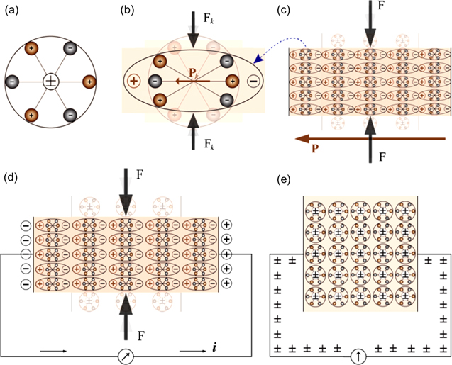
Figure 5. (a) No piezoelectric polarization, (b) the molecule subjected to an external force, (c) the polarization effect on the surface, (d) the piezoelectric material with two metal electrodes deposited on opposite surfaces, and (e) the reverse piezoelectric effect. Reproduced from [106]. CC BY 4.0.
Download figure:
Standard image High-resolution imageThe piezoelectric material, shown in figure 5(d), with two metal electrodes placed on opposing sides. When force is applied to the piezoelectric material surface, a constant charge density emerges on the surfaces of the crystal in contact with the electrodes if the electrodes are externally short-circuited, the galvanometer is linked to the short circuiting wire, and the electrodes are short-circuited externally. This polarisation produces an electric field, which in turn stimulates the conductor's free charges to flow. The free charges will migrate toward the ends where the fixed charges produced by polarisation are of the opposite sign, depending on their sign. As seen in figure 5(d), this flow of free charge continues until it cancels out the polarisation effect. This indicates that no charge flows regardless of the existence of external force in the steady state or the unperturbed state.
When the force acting on the material is released, polarisation also vanishes, the flow of free charges reverses, and the material returns back to its initial standstill state, as shown in figure 5(e). The current would travel via a resistance or load in place of the short-circuiting wire, converting mechanical energy into electrical energy. This plan is the cornerstone of several energy harvesting strategies that capture ambient mechanical energy, such as vibrations and transform it into a form that may be used by electrical devices [9]. The reverse piezoelectric effect, where a mechanical deformation results from the application of a voltage across the electrodes, can be seen in some materials. This method of producing mechanical strain can be utilised to move a connected mechanical load [124]. This process of converting electrical energy into mechanical energy that may be used is essential in applications like designing of nano positioning devices.
4. Piezocatalytic activity of TMDC semiconductors
So far, first principles calculations based on density functional theory (DFT) have been used to theoretically study the optical, electrical, and magnetic characteristics of several TMDC compounds [34, 127, 128]. Numerous experimental investigations [35, 37, 43, 129–136] have also been conducted, and the results show that MX2 (M=Mo, W and X=S, Se, Te) structures, which can be tuned in a broad range of ways by doping, strain, or electric field engineering, have such a great potential for a variety of technological applications. Additionally, the exceptional piezoelectric capabilities of TMDCs in the 2H crystal structure with D3h symmetry have led to their application in pressure sensors, transducers, high voltage generators, nonlinear energy harvesters, energy conversion, and piezotronic applications [35–37, 102, 129, 130].
First principles calculations were used by Duerloo et al to theoretically determine the piezoelectric characteristics of a single layer of BN, MoS2, MoSe2, MoTe2, WS2, WSe2, and WTe2 [34]. The relaxed-ion piezoelectric strain (d11) and stress (e11) coefficients of the 2H-TMDC monolayers are comparable or even superior to those of traditional bulk piezoelectric materials. Thorough theoretical analyses of the piezoelectric characteristics of semiconductor TMDCs and transition metal dioxide (TMDOs) monolayers have been carried out by Alyoruk et al indicates that these structures are excellent candidates for upcoming atomically thin piezoelectric applications [128]. TMDCs as layered materials are frequently non-centrosymmetric, and when an external force is applied to MoS2 and MoSe2 that are single- or odd-layered, an electric field is formed as a result of spontaneous polarization. This electric field effectively separates free carriers of electrons and holes to cause redox reactions on the surface [102].
4.1. Piezoelectric nanogenerator (PENG)
Using mechanically exfoliated MoS2 flakes, Wu et al have experimentally demonstrated PENG [35]. MoS2 flakes were embedded on a polymer stack, made up of water-soluble polyvinyl alcohol (PVA) and poly methyl methacrylate (PMMA) on a Si substrate. Figure 6(a) shows optical images of MoS2 flakes. Figure 6(b) depicts a schematic of working of single-layer MoS2 PENG device. As can be seen from figure 6(c), thin MoS2 flakes with an odd number of atomic layers exhibit oscillating piezoelectric voltage and current outputs as a result of cyclic stretching and releasing, whereas even-numbered flakes do not produce an output. Figure 6(d) illustrates the direct transformation of mechanical energy into electrical energy when strain is applied in the X direction (also known as the 'armchair' direction). Positive voltage and current output were observed with increasing strain, and negative output was observed with decreasing strain.
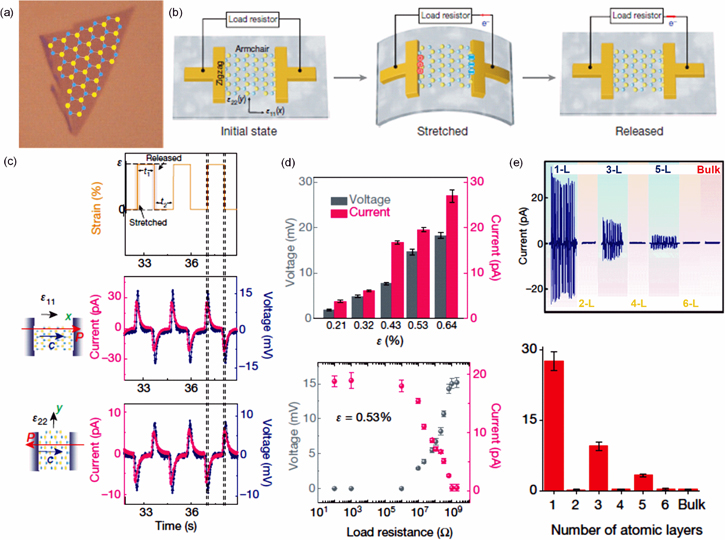
Figure 6. (a) Optical image of the single-atomic layer MoS2 flake, (b) schematic of the single-layer MoS2 device, (c) voltage and short-circuit current response of a single-layer MoS2 device under periodic strain in two different principal directions. Top: applied strain as a function of time. Middle: outputs from single-layer MoS2 when strain is applied in the x (armchair) direction. Bottom: outputs when strain is applied in the y (zigzag) direction, (d) dependence of voltage and current outputs from a single-layer MoS2 device. Top: as a function of a different strain. Bottom: under 0.53% strain as a function of load resistance, (e) observed outputs with the increasing number of atomic layers (n). Reprinted with permission from [35]. Copyright 2014 Nature Publishing Group, a division of Macmillan Publishers Limited. All Rights Reserved.
Download figure:
Standard image High-resolution imageWith the intensity of the applied tension, both reactions grew. Figure 6(d) demonstrates a single monolayer flake with a 0.53% strain producing a peak output of 15 mV and 20 pA, translating to a 2 mWm−2 power density and a 5.08% conversion efficiency. Due to the opposite orientation of the alternating layers in the most prevalent (2H) form of MoS2, samples with even numbers of flakes are predicted to be centrosymmetric and lose their piezo response (see figure 6(e)). The piezo response reappears in samples with an odd number of layers for the same reason.
It has been reported that the Piezoelectric polarization depends on the directions of principal strain in 2D materials [34, 35, 127, 128]

where i, j, and k can take the values 1, 2, and 3, with 1, 2, and 3 corresponding to the X, Y and Z axes, respectively, Pi
is the polarization and  are strain tensor. In the case of single-layer MoS2, there exists only one non-zero independent coefficient (e11). The in-plane polarization along the X-axis can be expressed as,
  whereas polarization along Y-axis is related to the pure shear strain e12 and can be ignored. A distinctive consequence of this symmetry using mechanically exfoliated MoS2 layers has been confirmed experimentally by Wu et al [35].
PENG using hydrothermally synthesized flowers-like MoSe2 nanostructure (FMN) and tube-like MoSe2 nanostructures have also been demonstrated recently [43]. The details of the synthesis mechanism and device fabrication can be found in reference 122. A schematic of the fabricated device is shown in figure 7(a). The device made with a tube-like MoSe2 microstructure, shown in figure 7(b), has the lowest open-circuit voltage (VOC), whereas FMN material-based PENG exhibits the greatest VOC of 2.12 V, which is almost 21 times higher. The FESEM images revealed that the tube-like MoSe2 microstructures are bulkier than flowers-like MoSe2 nanostructures (FMN), which results in reduced device response.
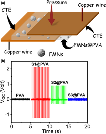
Figure 7. (a) Schematic of the fabricated PENG using FMN, (b) measurement of Voc of the fabricated devices at a particular periodic pressure as measured by digital storage oscilloscope. Reprinted with permission from [38]. Copyright 2021 Elsevier Ltd.
Download figure:
Standard image High-resolution imageAn electric polarisation is produced when a monolayer MoSe2 nanosheet is bent uphill or downward due to the displacement of the Mo ion (Z). The edge site of the nanosheet behaves as a cantilever beam with pressure applied at its free end when a periodic pressure is applied to the MoSe2 NF PENG. The spatial strain-induced lattice deviation of X, Y, and Z, respectively, is produced if the mechanical pressure operates along the X, Y, and Z axes. Thus, the density of flexoelectric polarisation (DFP) is produced as a result of strain gradients at structural boundaries [32, 38]. The DFP relies on the size and smaller the size of the nanosheets, the bigger the DFP. When N is the number of layers, the density of piezoelectric polarisation (DPP) and the DFP are both proportional to 1/N2. The piezoelectric voltage produced only from the piezoelectric polarisation, however, is small in the randomly distributed MoSe2 NF PENG. But the creation of piezoelectric voltage in this case has also been attributed to a strain-induced piezo-flexoelectric coupling phenomenon [43].
4.2. Piezocatalytic dye degradation
After the first experimental demonstration of piezoelectric properties of layered MoS2 [35], a lot of research work has been carried out on the piezocatalytic dye degradation properties of MoS2 and MoSe2 nanostructures [32, 36–41]. By coupling the piezoelectric and catalytic properties together, enhanced catalytic activity in the dark by hydrothermally synthesized MoS2 nanoflowers (NFs), shown in figures 8(a) and (b), has been demonstrated by Wu et al [36]. The piezoresponse force microscopy (PFM) indicates that a significant amount of piezoelectric potential generates on the edges of the abundantly single- and few-layer MoS2 NFs. The measured piezoelectric potential explains that an internal electric field is induced by a spatially spontaneous polarization from the single- and few-layer MoS2 and is responsible for the generation of the free carriers. This is consistent with the observed degradation of RhB with degradation efficiency ∼ 93% within 60 s (degradation rate 40 336 ppm l−1 mol−1 s−1) under the ultrasonic vibration in the dark, shown in figures 8(a)–(d). It has been reported by Wu et al [36] that the degradation activity of the commercial MoS2 bulk sheets and the TiO2 -P25 nanoparticles are poor (<8% degradation ratio) under the same experimental condition. An electric field is induced due to spontaneous polarization from the active surface sites of the MoS2 NFs, responsible for the high degradation efficiency [36, 137]. The MoS2 NFs possess an abundant odd number of layers with a noncentrosymmetric structure, and therefore under the mechanical-stress, a considerable piezoelectric potential is created for the release of an electric charge to separate the free electrons (majority carriers), and holes (minority carriers).
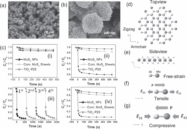
Figure 8. FESEM images of the MoS2 NFs (a) low magnification, (b) high magnification, (c) the degradation ratio of RB dye using the MoS2 NFs, commercial MoS2 and TiO2 -P25 (i) in dark, (ii) ultrasonic wave assistance in dark, (iii) the cyclic degradation tests of RB dye using the MoS2 NFs under ultrasonic-wave in the dark, (iv) The degradation ratio of RB dye under ultrasonic-wave assistance with the xenon-lamp illumination using the MoS2 NFs. The atomic structure of the MoS2 is in (d) top view, and (e) bottom view, the lower part is Mo-2S dipoles in a free-strain state, (f) spontaneous polarization of the Mo-2S dipoles due to the expansion in the +X-axis, (g) spontaneous polarization of the Mo-2S dipoles due to compression in the +X-axis. Reprinted with permission from [27]. Copyright 2016 John Wiley & Sons.
Download figure:
Standard image High-resolution imageThe MoS2 demonstrates a single Mo layer sandwiched between two S layers with a bond length of Mo–S 2.418 Å to create a hexagonal shape because of the crystalline D3h symmetry. Figures 8(e) and (f) demonstrate the asymmetrical construction of each unit cell, which consists of one Mo atom on the right and two S atoms. The induced electric field propagates and is aligned with the X direction when the Mo-2S dipoles are stretched, as illustrated in figure 8(g). Spontaneous polarisation is formed from the S site to the Mo site along with the armchair direction (for example, +X direction). As illustrated in figure 8(h), the opposing electric field in +X direction is produced when the Mo-2S dipoles undergo compressive strain, which causes the polarisation to point from the Mo site to the S site [36, 138]. The direction of the external force is mirrored by the spontaneous polarization-induced propagation of the electric field. The separation of the free carriers of the electron and hole in the opposite direction is effectively pushed by the electric field.
The polar dye molecules are effectively driven to adsorb on the active surface sites by the piezoelectric potential created as a result of piezoelectric polarisation under external mechanical stress. As a result, as mentioned previously, the potential energy may be used to modify the bending of the MoS2 bands. The total strain-induced potential energy shift across the semiconductor is given by [36, 139]

where,  denotes the applied stress in n dimension, Wx is the width of MoS2 in the X direction, εrx
is the relative permittivity in the X direction, and dxn
, also known as the piezoelectric coefficient,
denotes the applied stress in n dimension, Wx is the width of MoS2 in the X direction, εrx
is the relative permittivity in the X direction, and dxn
, also known as the piezoelectric coefficient,  represents the permittivity of free space or electric constant. Therefore, the essential parameters for calculating the total potential energy (Vp) are the piezoelectric coefficients dxn
and σn
. The amount of electric field that may be produced by mechanical stress depends on the potential energy Vp. The larger the value of Vp, the more the polar molecules can be induced to be absorbed on the semiconductor's surface, and the higher band bending could be formed.
represents the permittivity of free space or electric constant. Therefore, the essential parameters for calculating the total potential energy (Vp) are the piezoelectric coefficients dxn
and σn
. The amount of electric field that may be produced by mechanical stress depends on the potential energy Vp. The larger the value of Vp, the more the polar molecules can be induced to be absorbed on the semiconductor's surface, and the higher band bending could be formed.
Thakur et al [42] examined the piezocatalyst, photocatalyst, and piezophototronic effect of CVD-grown monolayer WS2 on the sapphire substrate, depicted in figure 9(a). The CVD-grown WS2 layer has been used to demonstrate ultrafast photodecomposition of organic dyes as well as an antibacterial activity through the piezophototronic effect. PFM microscopy measurement was carried out to confirm the piezoelectric polarization. Piezocatalysis experiment has been carried out using a WS2 monolayer over an Al2O3 substrate along with an MB solution, in a sonicator, shown in figure 9(b). The rate constant for monolayer WS2 on Al2O3 was 0.017 16 min−1. Al2O3 and bare MB dye had piezoelectric rate constants of 0.001 20 and 0.001 09 min−1, respectively, which are very less than WS2 on Al2O3, as shown figure 9(c).

Figure 9. (a) (i) Optical image demonstrating the growth of monolayer WS2 on the sapphire substrate, (ii) optical image with high magnification displaying distinct WS2 domains, (iii) FL image of monolayer WS2, (b) the UV–visible spectroscopy-based time-dependent piezocatalytic degradation of MB in a 2D WS2 monolayer, (c) piezocatalytic dye degradation rate study, (d) a WS2 monolayer's catalytic cyclic performance, (e) scavenger test on the piezocatalytic dye degradation efficiency, (f) degradation reaction kinetics of a 2D WS2 monolayer using photocatalysis, piezocatalysis, photo-piezocatalysis, and (g) a 2D WS2 monolayer's photopiezocatalytic performance. Reprinted with permission from [42]. Copyright 2021, American Chemical Society.
Download figure:
Standard image High-resolution imageAl2O3 has been chosen for better adhesion of WS2 with Al2O3 than other substrates, e.g. SiO2/Si and Si, as demonstrated by Thakur et al [42]. Figure 9(d) shows that even after 3 cycles, degradation efficiency (∼80%) remains almost constant. Piezocatalytic dye degradation experiments have also been carried out using different scavengers and the corresponding degradation efficiencies are shown in figure 9(e). This experiment indicates that the degradation efficiency is highest in the absence of any scavenger. In WS2 with odd number of layers, the W and S atoms are moved due to external tension. This displacement results in piezoelectric polarisation and electric dipole generation. Piezoelectric effect has been coupled with photocatalysis to enhance the charge separation and thereby degradation efficiency. When piezo-photocatalysis is combined, as illustrated in figure 9(f), MB dye is degraded more quickly than when piezo- or photocatalysis is used alone. The corresponding dye degradation efficiencies are shown in figure 9(g). The reported rate constant values using photocatalysis, piezocatalysis, and combined piezo-photocatalysis are 0.0134, 0.0171, and 0.0280 min−1, respectively. Because the polarisation effect and photogenerated charge carriers effectively separate charges, it has been hypothesised that coupled photo-piezocatalysis is a significantly quicker process [140–143].
Piezocatalytic degradation of organic pollutants (tetracycline and RhB) under periodic local mechanical strain provided by ultrasonic vibration by few-layer TMDC materials (MoS2, WS2, and WSe2), shown in figure 10(a), has recently been studied by Li et al [41]. PFM microscopy measurements have been done and theoretical calculations of the piezoelectric stress coefficients (e11) have also been estimated for a better understanding of the piezocatalytic mechanism. The degradation rate of RhB and tetracycline for 3 cycles with MoS2, WS2, and WSe2 are shown in figures 10(b) and (d), respectively. The degradation efficiency of RhB with MoS2, WS2, and WSe2 nanosheets are ∼ 96%, 65.7%, and 43.5%, respectively, after 60 min of ultrasonic vibration. For the tetracycline solution, the degradation efficiencies are ∼93%, 71%, and 62% for MoS2, WS2, and WSe2, respectively. The corresponding reaction kinetics rates are shown in figures 10(c) and (e). Degradation reaction kinetics using different scavengers are shown in figures 10(f)–(h) for few layers MoS2, WS2 and WSe2, respectively. Because of negligible piezoelectric response in bulk TMDs nanosheets, the commercial bulk samples show very weak degradation activity.
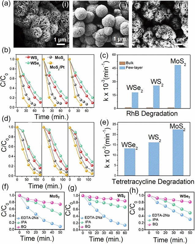
Figure 10. (a) Typical SEM images of three types of TMDC nanosheets with few layers: (i) MoS2, (ii) WS2, and (iii) WSe2. Three cycle tests of the piezocatalytic activity for (b) RhB solution, (c) RhB degradation reaction kinetics and (d) tetracycline solution, (e) tetracycline degradation reaction kinetic rates under ultrasonic vibration using few-layer (blue) or bulk (orange) TMDs samples. Scavenger test using (f) MoS2, (g) WS2, and (h) WSe2 layers. Reprinted with permission from [41]. Copyright 2019 Elsevier Ltd.
Download figure:
Standard image High-resolution imageThe piezocatalytic activities of the different TMDC samples have been carried out by water spilling for H2 evolution under ultrasonic vibration. All the three samples can produce H2 from water under ultrasonic vibration having evolution activity MoS2 > WS2 > WSe2, as shown in figures 11(a)–(d). The strong correlation between these findings and the PFM analyses leads one to believe that the piezopotential caused by ultrasonic vibration is a key factor in the catalytic performance of these systems. As proposed by Li et al, under external stress, the dipole moment induces polarised positive and negative charges on the two sides of the piezoelectric 2D TMDC materials [41]. This creates a polarisation electric field across the nanosheets and causes free electrons and holes to move in opposite directions. The holes are eventually trapped by H2O at the surface to produce •OH radicals and the electrons combine with the dissolved O2 to produce •O2−. In the aqueous solution, these free radicals can oxidise RhB or tetracycline molecules which can be used to split water and degrade organic pollutants [41]. Their piezocatalytic capabilities can also be enhanced by adding nanoparticles of heavy metals like Pt and Au. Based on the above results and analysis, amechanism has been proposed to illustrate the piezocatalytic processes, shown in figures 11(e)–(g).

Figure 11. (a) Few-layer TMD nanosheets are used to produce H2 under ultrasonic vibration, (b) the corresponding H2 evolution rate, (c) the amount of H2 that developed when bulk MoS2, MoS2 nanosheets, MoS2 nanosheets/Pt, and MoS2 nanosheets/Au were subjected to ultrasonic vibration, (d) cyclic piezocatalytic H2 production test of MoS2 nanosheets, (e) monolayer 2H-phase MX2 with top and side views (M=Mo, W; X=S, Se). The blue arrows indicate the piezoelectric polarization's orientation, (f) schematic depiction of the catalytic processes caused by the piezopotential in a few layer TMD nanosheets when mechanical force is applied, (g) calculated band energy level diagrams of MoS2, WS2, and WSe2 are compared to the potentials for oxidation and reduction of water (dotted lines). Reprinted with permission from [41]. Copyright 2019 Elsevier Ltd.
Download figure:
Standard image High-resolution imageSynthesis of piezocatalytic MoS2 nanoflower (NFs) has been demonstrated by Lin et al [31]. MoS2 NFs possess abundant single- and odd few-layers, shown in figures 12(a)–(b), which are the main component to dominate the piezocatalytic activity. The PFM microscopy was used to assess the piezo-electric potential of the MoS2 NFs. To ensure their degrading activity under ultrasonic vibration in the dark, the MoS2 NFs were enclosed in PDMS films with various catalysts, including the MoS2 NFs, commercial MoS2 sheets, TiO2-P25 nanoparticles (size 20 nm), and blank PDMS films. Figures 12(c)–(e) demonstrate the considerable degrading activity of MoS2 NFs/PDMS film in contrast to TiO2-P25/PDMS film and the blank PDMS film. Electron mobility and concentration have been measured by Hall measurement to better understand the piezocatalytic mechanism. According to the results of the Hall measurement, the single-layer MoS2 has been found to have predominant VS (single sulphur vacancy) and/or V2S (double sulphur vacancy), thereby inducing localized donor states inside the bandgap [31, 144–146]. After being strained, the Mo–S dipoles align their polarisation from S to Mo. By doing this, the e−-h+ pair separation is produced by an electric field that propagates in a zigzag or armchair direction [31]. The interaction with the water molecules is then started by the electrons and holes being split in opposing directions. As a result, the water molecule with the positive ends will be forced to be absorbed on the surface with the Mo–S dipoles' negative charge ends, whereas the water molecule with the negative ends will be tripped by the dipoles' positive charge ends [31]. The numerous radical species, such as free radical oxygen, hydroxyl radical, and hydrogen peroxide, will be produced by the absorbed polar molecule on the MoS2/PDMS to decompose the dye solution [31, 137].
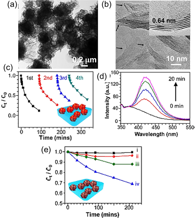
Figure 12. (a) TEM image of the MoS2 nanofibers, (b) a single- and few-layer structure, (c) testing the RhB dye's cyclic deterioration while employing MoS2 NFs and ultrasonic shaking in the dark, (d) measuring the intensity of the OH radicals at 0, 5, 10, 15, and 20 min, (e) the rate of RhB dye degradation in PDMS, commercial MoS2 sheets in PDMS, TiO2-P25 in PDMS, and MoS2 NFs in PDMS when subjected to ultrasonic vibration in the dark. Reprinted with permission from [31]. Copyright 2016 Elsevier Ltd.
Download figure:
Standard image High-resolution imageRecently, it has also reported the ultrafast piezocatalytic degradation of organic dyes by using flower and tube like nanostructures of MoSe2 synthesized by hydrothermal method [38]. The piezoelectric properties of the synthesized samples, shown in figures 13(a)–(c), have been verified through the fabrication of a PENG, as discussed earlier in section 4.1. Under low-frequency ultrasonic irradiation, the synthesised FMNs have been employed as active piezocatalytic dye degradation materials. Figures 13(d)–(f) depict the degradation of RhB dye by various FMN samples when subjected to continuous ultrasonication in the dark. As shown in figure 13(g), it has been observed that with RhB dye solution, the piezocatalytic dye degradation efficiency is ∼86% in 60 s with a reaction rate constant (k) of 0.104 s−1. The FMNs also exhibit degradation efficiency of ∼85% in 60 s with MB dye solution. The FMNs also show remarkable piezocatalytic abilities when used with an RhB and MB dye combination (1:1). Under mechanical vibration, Mo-2Se dipole, generated due to a periodic uniaxial strain, as shown in the schematic in figure 13(h), induces an electric field. This multi-directional mechanical strain at different places provides piezoelectric potential in diverse directions, resulting in a spontaneous polarisation directed from Se to Mo and forming a noncentrosymmetric MoSe2 FMN [44, 147, 148]. In order to degrade organic dyes, this electric field promotes the production of superoxide (•O2−) and hydroxyl (•OH) radicals, thus facilitating the process of degrading organic dyes [38].
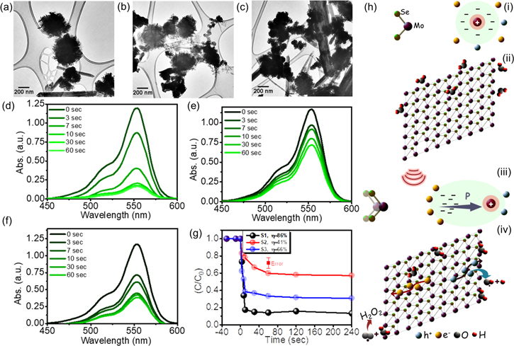
Figure 13. TEM images of the synthesized samples: (a) S1 (sample obtained after a 4 h reaction time), (b) S2 (sample obtained after an 8 h reaction time), and (c) S3 (sample obtained by 12 h reaction time), (d)–(f) piezocatalytic degradation of RhB dye under continuous ultrasonication in the dark by samples S1, S2, and S3, respectively, (g) the degradation profiles of the RhB dye for the S1, S2, and S3 samples, respectively, (h) the schematic of (i) the Mo-2Se dipoles in the free-strain state without polarisation, (ii) the randomly distributed free carriers on the surface of MoSe2 under no mechanical strain, (iii) the polarised Mo-2Se dipoles (aligned from the Se to the Mo site under the applied mechanical strain), and (iv) the creation of (e−-h+) pairs in the surface charge region. Reprinted with permission from [38]. Copyright 2021 Elsevier Ltd.
Download figure:
Standard image High-resolution imageMa et al reported multi-flaw and flaw-free MoS2 piezoelectric materials, shown in figure 14(a), synthesized via a simple hydrothermal method [149]. The piezocatalytic activities of multi-flaw MoS2, flaw-free MoS2, and commercial MoS2 were evaluated for the degradation of Ciprofloxacin (CIP), a third-generation antibiotic, under ultrasonic vibration. Prior to ultrasonic vibration, the adsorption of CIP in the presence of multi-flaw MoS2 reached only 39%, shown in figure 14(b). The multi-flaw MoS2 nanosheets show the highest piezocatalytic activity with a degradation rate of ∼99% within 30 s of ultrasonication. Due to the presence of several odd-numbered layers in multi-flaw MoS2 nanosheets, a piezoelectric effect caused by inversion symmetry breaking has been produced. The many MoS2 structural faults also boosted asymmetry and electron density, leading to strong piezocatalytic performance for CIP degradation. The longitudinal acoustic waves that make up ultrasonic waves, as shown in figures 14(c)–(i), travel with periodic cycles of compression and rarefaction. Ultrasonic waves having a wavelength of several μm can induce significant polarization in nanostructures.

Figure 14. (a) SEM images of multi-flaw MoS2 in (i) low- and (ii) high-resolution, (iii) flaw-free MoS2, (iv) commercial MoS2, (b) the piezocatalytic performance of free-flaw and multi flaw MoS2 under ultrasonic vibration, (c) (i) acoustic pressure change as the ultrasonic wave travels through a material, (ii) a side view of MoS2's atomic structure, (iii)–(iv) schematic representations of the uniaxial strain caused by ultrasonic pressure, and how it affects the polarisation potential. The 'armchair' direction of the MoS2 monolayer is represented by the orthogonal coordinate system's X-direction, while the 'zigzag' direction is represented by the orthogonal coordinate system's Y-direction, (v) and (vi) diagrammatic representations of the local isotropic strain caused by ultrasonic pressure and how it affects the polarisation potential. The red arrows represent the direction of polarization. The blue arrows represent the direction of the applied force. Reprinted with permission from [149]. Copyright 2018 Royal Society of Chemistry.
Download figure:
Standard image High-resolution imageAdjacent sites in a honeycomb structured hexagonal 2H MoS2 are occupied by Mo and S atoms. Each unit cell is asymmetrically formed by one Mo atom on the left and two S atoms on the right side, as shown in the corresponding side-view crystallography in the schematic, Scheme 14(c-ii). The centres of the positive and negative charges meet at the same location with the dipole moment zero when there is no strain. As a result, the crystal has no polarisation potential. Periodic uniaxial strain (along the X- or Y-axis) and locally isotropic strain (along the Z-axis) is likely imparted to MoS2 when it is submerged in water while being vibrated by ultrasonic waves, causing internal polarisation in the MoS2 nanosheets [143, 149]. Distinct mechanical strain orientations and locations produce different piezoelectric potentials. Negative polarisation charges are generated on the zigzag edges of MoS2 at the left-hand surface and positive polarisation charges are induced at the right-hand surface when MoS2 is subjected to tensile strain in the armchair direction [149], shown in figures 14(c-iii). The crystal experiences a potential drop in the direction of the strain. However, when MoS2 is subjected to compressive strain, shown in figures 14(c-iv), the honeycomb structure is condensed and the spontaneous electric field is produced in the +X direction, which is the opposite of the original orientation. Diagrammatic representations of the local isotropic strain caused by ultrasonic pressure and its effect on the polarisation potential are shown in figures 14(c-v) and (c-vi).The edges of MoS2 nanosheets tend to accrue spontaneous polarisation charges (e− and h+), which are separated by the internal electric field and start the redox process that breaks down CIP [149, 150].
4.3. Piezocatalytic hydrogen evolution reaction (HER)
Recently, the piezoelectric effect of WS2 to improve its HER catalytic performance has been reported by Zhang et al [44] Few-layer WS2 nanosheets have been synthesized by a simple liquid phase stripping method, the piezoelectric activity and thickness of the synthesized nanosheets were measured by PFM and AFM microscopy images. The non-centrosymmetric structure of the WS2 nanosheets, shown in figure 15(a), result in improved piezoelectric characteristics. Due to the ultrasonic vibration, a few layer WS2 nanosheets distort, and the piezoelectric action causes a polarised electric field to generate on the surface. Figure 15(b) illustrates how a polarised electric field will cause some positive and negative charges to travel to the opposite sides of WS2 nanosheets. In the macroscopic perspective, charges build up on the WS2 nanosheets' opposing surfaces to create a potential difference. The HER process will be aided by the negative charge's ability to draw free hydrogen ions from the electrolyte and produce hydrogen as a result.
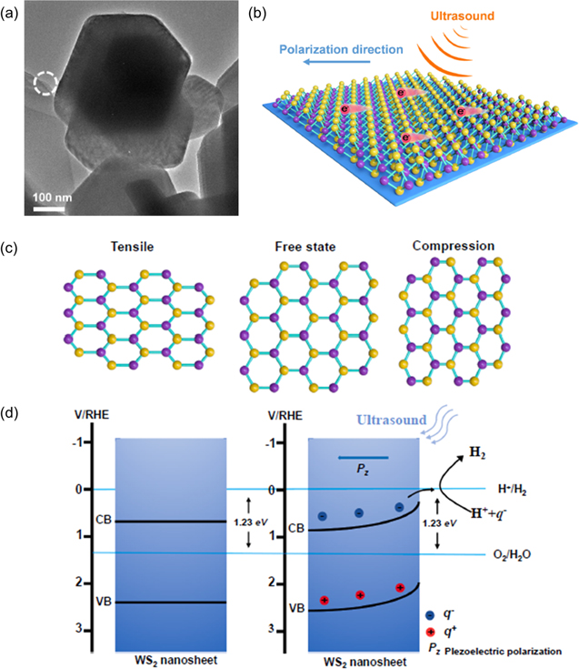
Figure 15. (a) TEM image of WS2 nanosheets, (b) schematic illustration of the piezoelectric catalysis of WS2 nanosheets under the influence of ultrasonic energy, (c) top view of the WS2 monolayer's atomic structure under ultrasonic energy. The centre is not stressed, but the left and right sides are squeezed and stretched, respectively. (d) a schematic showing how an ultrasonic vibration-induced band tilt is produced. Reprinted with permission from [44]. Copyright 2021 Elsevier Ltd.
Download figure:
Standard image High-resolution imageA schematic diagram of atomic piezoelectricity and a schematic illustration of energy band tilt due to ultrasonic vibration are shown in figures 15(c)–(d). W and S atoms are coordinated in a hexagonal shape as shown in figure 15(c). In a free state without tension, the W and S positive and negative ion centers overlap each other, as shown in the middle. When subjected to tensile (figure 15(c), left) or compression (figure 15(c), right) stress due to ultrasound, W4+ center and S2− center are displaced. Therefore, during deformation, dipole moments are generated due to the relative displacement between the cation and anion centers. Macroscopic piezoelectric potential is created when dipole moments generated by all units in the crystal are superimposed, which promotes the piezoelectric activity. Energy band tilts under vibration induced piezoelectric field, as shown in figure 15(d). In absence of mechanical vibration, the CB and VB of WS2 is shown in figure 15(d) (left). WS2 nanosheets will be easily bent due to mechanical vibration. Many negative and positive charges produced around the catalyst surface due to vibration induces piezoelectric field, which will cause CB and VB to bend, as shown in figure 15(b) [115, 151].
The free layer-dependent piezoelectricity of O doped MoS2 synthesized by solvothermal method for enhanced piezocatalytic HER from pure water has recently been reported by Lei et al [45]. SEM images of MoS2 and O-doped MoS2 are shown in figure 16(a). Figure 16(b) illustrates the piezocatalytic H2 generation from pure water under ultrasonic irradiation that has been used to assess the piezocatalytic activity of the as-prepared samples. From the PFM images and amplitude butterfly loop, the estimated piezoelectric response of O doped MoS2 is ∼ 9.45 pm V−1, which is larger than that of MoS2 (4.74 pm V−1).

Figure 16. (a) SEM images of (i) MoS2 and (ii) O-MoS2, (b) the H2 production rate under ultrasonic vibration, (c) the atomic structure of O-MoS2 in (i) side view (ii) free-strain state (iii) Spontaneous polarization of MoOx -Mo–S, O–Mo–S, and S–Mo–S under tensile and compressive strain, (d) the schematic diagram of piezocatalytic H2 production over O-MoS2 nanosheets from H2O. Reprinted with permission from [45]. Copyright 2021 Elsevier.
Download figure:
Standard image High-resolution image
The side view and free-strain state dipole moment of O doped MoS2, are shown in figures 16(c) (i) and (ii), respectively. MoOx -Mo–S, O–Mo–S, and S–Mo–S will all have a different dipole moment when O-MoS2 is exposed to an external force. As seen in figures 16(c) (iii), when the MoOx -Mo–S dipole moment is stretched, the spontaneous polarisation (P) that results points from MoOx , S to Mo and the direction of polarisation is deflected by an angle from X-direction to Z-direction, inducing out-of-plane polarisation that is advantageous for the transfer of free electrons and holes to the OMoS2 basal plane. The direction of polarisation is reversed when the MoOx -Mo–S dipoles are compressed compared to when they are extended. Similar to this, when the O–Mo–S dipoles are stretched, spontaneous polarisation from O, S to Mo is created, and the polarization's direction is deflected by an angle β from the X-direction to the Z-direction, where β is smaller than α. When the S–Mo–S dipoles are stretched, spontaneous polarisation pointed from 2S to Mo together with the X-direction is formed when the O–Mo–S dipoles are compressed; the resulting spontaneous polarisation is pointed from Mo to O, S (armchair direction). The direction of polarisation is reversed when the S–Mo–S dipoles are compressed in compared to when they are extended. Unidirectional charge separation is effectively pushed along by the electric field created by spontaneous polarisation.
Materials get deformed when they are subjected to ultrasonic vibration, and piezoelectric fields have resulted from the alteration in the dipole moment. As mentioned earlier, the piezoelectric field might also tilt the band, causing band bending. Equation (7) may be used to get the band bending force (Vp). In this instance, Vp for MoS2 is 0.33 V whereas it is 0.36 V for O-MoS2, showing that O-MoS2 produces a higher piezoelectric potential than MoS2 when the same stress is applied. The 'cavitation effect', which is caused by an ultrasonic wave's longitudinal nature, is the creation of a large number of small vacuum bubbles under the pressure shift it causes in a liquid. When the bubbles reach their critical and unstable size, they finally burst, releasing a tremendous amount of pressure (108 Pa) [2]. According to figure 16(c), the pressure transits to the surface of O-MoS2, where it is likely subjected to periodic uniaxial strain (along the X- or Y-axis) and locally isotropic strain (along the Z-axis), which results in the tensile or compression of the dipole moment in MoOx -Mo–S, O–Mo–S, and S–Mo–S. The accompanying spontaneous polarisation field is generated by a change in the dipole moment. Figure 16(d) illustrates a potential process for piezocatalytic H2 generation from clean water using O-MoS2. A brief summary of the TMDC materials used as piezocatalyst is summarized in table 1.
Table 1. A brief summary of the TMDCs nanomaterials as piezocatalysts.
| Sl. No. | Materials | Synthesis method | Main findings/applications | References |
|---|---|---|---|---|
| 1 | MoS2 flakes | Mechanical exfoliation | Piezocatalytic nanogenerator (PENG) | [35] |
| 2 | Flowers-like MoSe2 nanostructure (FMN) and tube-like MoSe2 nanostructures | Hydrothermal synthesis | Piezocatalytic nanogenerator (PENG) and Piezocatalytic dye degradation | [38] |
| 3 | MoS2 nanoflowers (NFs) | Hydrothermally synthesis | Piezocatalytic dye degradation (RhB Dye) | [36] |
| 4 | Monolayer WS2 on the sapphire substrate | Chemical vapour deposition (CVD) | Piezo−Phototronic Dye Degradation and Bacterial Disinfection | [42] |
| 5 | Few-layer TMDC materials (MoS2, WS2, and WSe2) | Solvothermal method | Piezocatalytic degradation of organic pollutants (tetracycline and RhB)- by adding heavy metals, piezocatalytic activities can be enhanced (e.g. Pt and Au) | [41] |
| 6 | Single- and few-layers MoS2 nanocomposite | Hydrothermal process | Piezocatalytic dye degradation (RhB Dye) | [31] |
| 7 | Multi-flaw and flaw-free MoS2 nanosheets | Hydrothermal process | Super-high piezocatalytic activity for the decomposition of Ciprofloxacin (CIP) | [149] |
| 8 | 2D few-layer WS2 nanosheets | Liquid phase stripping method | Piezo-catalytic enhanced hydrogen generation | [44] |
| 9 | MoS2 and Oxygen-doped MoS2 nanosheets | Solvothermal method | O doped MoS2 displays superior piezocatalytic hydrogen generation from pure water. | [45] |
5. Challenges and prospective- conclusions and outlook
TMDC piezocatalytic materials recently emerged as promising mechanical-energy-triggered catalytic materials having huge potential to be applied in different areas, such as wastewater purification, water splitting, and sterilization. A brief summary of piezocatalytic dye degradation activity and HER activity using different TMDCs are presented in table 2.
Table 2. Piezocatalytic dye degradation activity and HER activity using different TMDCs.
| Sl. no. | Materials | Catalytic conditions | Dye tested | Reaction rate | Degradation efficiency | HER activity | References |
|---|---|---|---|---|---|---|---|
| 1 | MoSe2 nanoflowers | Ultrasonic + dark | Malachite green | — | 85% | — | [26] |
| 2 | Single and few-layers MoS2 Nanoflowers | Ultrasonic (40 kHz) + dark | RhB | 40336 ppm L mol−1s−1 | ∼93% | — | [27] |
| 3 | single- and few-layered MoSe2 nanoflowers | Ultrasonic (40 kHz) + dark | RhB | 69,889 ppm L mole−1 s−1. | 90% | — | [28] |
| 4 | Single- and few-layers MoS2 nanocomposite | Ultrasonic (40 kHz) + dark | RhB | — | ∼99% | — | [31] |
| 5. | Quartz microrods@ few-layered MoS2 hierarchical heterostructure | Ultrasonic (25–40 kHz) + dark | RhB | — | ∼99% | ∼90% 6456 μmol g−1h−1. | [32] |
| 6 | Defect-rich MoS2 | Ultrasonic+Dark | RhB | 0.01597 min−1 | 64.1% | — | [37] |
| 7 | Flower and tube-like MoSe2 nanostructures | Ultrasonication (40 kHz) + dark | RhB | 0.104 s−1/0.013 s−1/0.058 s−1 | ∼86%,/41%,/ 66% | — | [38] |
| 8 | Few layer MoS2, WS2, and WSe2 | Ultrasonic + dark | RhB | 96% (MoS2) 65.7% (WS2) 43.5% (WSe2) | — | — | [41] |
| Tetracycline | 93% (MoS2), 71% (WS2), and 62% (WSe2) | — | 29.2 μmol g−1 h−1 (MoS2) 11.3 μmol g−1 h−1 (WSe2) | ||||
| 9 | Monolayer WS2 on Al2O3 substrate | A visible-light source of 15 W | MB | 0.0134 min−1 | — | — | [42] |
| Ultrasonic (40 kHz) + dark | MB, RhB and MO | 0.0171 min−1 | ∼87% MB ∼85% RhB ∼ 82% MO | — | |||
| Ultrasonic (40 kHz) + A visible-light source of 15 W | MB | 0.0280 min−1 | — | — | |||
| 10 | Oxygen-doped MoS2 | Ultrasonic (40 kHz) + Dark | — | — | — | 47.75 μmol·h−1 g−1 | [45] |
| 11 | Hybrid 1T- and 2H-Phase Few-Layered MoSe2 Nanosheets | Ultrasonic (20–60 kHz) and different levels of power (120–300 W) | — | — | — | 5000 μmol g−1 h−1. | [129] |
| 12 | Multi-flaw MoS2 nanosheet | Ultrasonic + Dark | Ciprofloxacin | 1.29 l mg−1 s−1 | 99% | — | [149] |
In this review, the recent advances in TMDC nanomaterials-based piezocatalysis have been discussed. The currently developed TMDC piezocatalysts and piezo-photocatalysts are still far from practical applications in ambient conditions. Future uses of these technologies are severely constrained by their ineffective mechanical energy collection and poor recycling. To achieve practical piezocatalysis, the sensitivity of piezocatalysts or piezo-photocatalysts to mechanical stress should be increased. The materials' piezoelectric characteristics are more significant than their morphological structure (1D or 2D). For a material to be piezocatalytically active, the presence of free charges is important. The best piezocatalysts are piezoelectric materials with high carrier densities and piezoelectric coefficients. In the process of piezocatalysis, the inherent charge carrier density is crucial for charge transfer. Most piezo/piezo-photocatalytic reactions to date have been conducted under intense ultrasonic vibration, which is seldom present naturally. It has also been observed that the size and structures of the nanomaterials affect the piezocatalytic efficiency. Sometimes piezocatalysis together with photocatalysis is found to be more useful. The piezocatalytic mechanism in TMDCs has not been understood in detail so far. Various proposed mechanisms are discussed in brief in this review. The applications of piezocatalysts or piezophotocatalyst are mainly confined now-a-days to the degradation of pollutants and water splitting. More applications, such as nitrogen fixation, CO2 reduction, selective organic synthesis, medical treatment, etc are highly desired.
Additionally, heavy metal nanoparticles (such as Au and Pt) that operate as the electron sink to assist the transport of electrons from the TMDCs to metal in such heterojunction systems can be deposited to further enhance the piezocatalytic activity of TMDC materials. In comparison to electrocatalysis or even photocatalysis energy conversion methods, piezocatalytic activity in TMDC materials is still rather low since the research into this effect is still in its early stages. Additionally, there are a number of fundamental difficulties that are still poorly understood. Piezoelectrics need to balance conductivity and piezoelectricity in order to function well as catalytic materials.
To further understand the piezocatalytic effects, it would be beneficial in the future to carefully manage the layer numbers and phases (1T and 2H) of TMDCs materials and to look into their conductivity and piezoelectricity properties. The future catalytic and photocatalytic systems for environmental remediation may be developed by using piezoelectric materials alone or in combination with other materials as a replacement.
Acknowledgments
Authors acknowledge the partial financial support from CSIR, Govt. of India with Grant No. 03(1472)/19/EMR-II dt. August 05, 2019. We are very much grateful to numerous authors and researchers whose research articles/books have been referred and there may be some which we could not include in the reference list due to lack of space etc but we have been benefited from them greatly to learn the subject and we would like to duly acknowledge their contributions too. We are thankful to the Editorial team for the Invitation and to the reviewers for their fruitful suggestions/comments.
Data availability statement
The data cannot be made publicly available upon publication because they are owned by a third party and the terms of use prevent public distribution. The data that support the findings of this study are available upon reasonable request from the authors.
Declaration of competing interest
The authors declare that they have no competing financial interest or personal relationships that could have appeared to influence the work reported in this paper.
Ethical statement
This work does not include studies on human subjects, human data or tissue, or animals.