
Abstract
Self-powered broadband photodetectors have attracted great interest due to their applications in biomedical imaging, integrated circuits, wireless communication systems, and optical switches. Recently, significant research is being carried out to develop high-performance self-powered photodetectors based on thin 2D materials and their heterostructures due to their unique optoelectronic properties. Herein, a vertical heterostructure based on p-type 2D WSe2 and n-type thin film ZnO is realized for photodetectors with a broadband response in the wavelength range of 300–850 nm. Due to the formation of a built-in electric field at the WSe2/ZnO interface and the photovoltaic effect, this structure exhibits a rectifying behavior with a maximum photoresponsivity and detectivity of ∼131 mA W−1 and ∼3.92 × 10¹⁰ Jones, respectively, under an incident light wavelength of λ = 300 nm at zero voltage bias. It also shows a 3-dB cut-off frequency of ∼300 Hz along with a fast response time of ∼496 μs, making it suitable for high-speed self-powered optoelectronic applications. Furthermore, the facilitation of charge collection under reverse voltage bias results in a photoresponsivity as high as ∼7160 mA W−1 and a large detectivity of ∼1.18 × 10¹¹ Jones at a bias voltage of −5 V. Hence, the p-WSe2/n-ZnO heterojunction is proposed as an excellent candidate for high-performance, self-powered, and broadband photodetectors.
Export citation and abstract BibTeX RIS

Original content from this work may be used under the terms of the Creative Commons Attribution 4.0 licence. Any further distribution of this work must maintain attribution to the author(s) and the title of the work, journal citation and DOI.
1. Introduction
Photodetectors, which convert incident photons into electrical signals, play an important role in many applications including biological/medical imaging [1], optical telecommunications [2], environmental monitoring [3], astronomical observations [4], and integrated circuits [5]. Traditional photodetectors require an external bias to produce a detectable photocurrent, limiting their performance in terms of dark current [6], circuit noise [7], and power consumption [8]. On the other hand, self-powered photodetectors (SPPDs) can detect the optical signals without applying an external bias voltage based on three mechanisms: (I) photovoltaic effect in the p–n or the Schottky junction-based photodetectors [9, 10]; (II) pyro-phototronic effect in the pyroelectric-based photodetectors [4]; (III) tribo-phototronic effect in the triboelectric nanogenerators [11]. SPPDs have a wide range of applications such as solar cell technology [9], gas sensors [12, 13], and remote sensing [14].
Recently, SPPDs based on 2D transition metal dichalcogenides (TMDs) and their heterostructures have attracted great attention due to their ultrahigh photoresponsivity [15], fast response [16], and broadband detection [1]. These device properties can be attributed to the high absorption coefficient, suitable bandgap for photovoltaic application, and high electron mobility of TMDs [9, 17]. The p–n junction is the building block of photovoltaic SSPDs [18]. In the p–n junction-based SPPDs, the photo-generated electron/hole carriers can be separated by the built-in electric field at the interface of p-type and n-type 2D materials [19]. The p–n junction can be formed in a single 2D material using chemical doping [20] and double electrostatic gating [21]. However, creating a p–n homojunction with high stability using these methods is challenging and complicated [20, 22]. Alternatively, various p–n heterojunctions based on two different 2D materials, such as WSe2, and other nanostructures can be fabricated by transfer techniques [23] with desirable band alignments and optoelectronic performance [1]. For instance, Chen et al [24] has reported a SPPD based on WSe2/GaAs 2D/1D with a responsivity of ∼123 mA W−1 at an incident light wavelength of 532 nm. A SPPD device with a maximum photoresponsivity of ∼100 mA W−1 based on WSe2/graphene 2D/2D structure has also been reported [25]. In another work, Zhang et al [26] has reported a broadband SPPD based on WSe2/Si 2D/3D vertical heterojunction with a maximum photoresponsivity of 294 mA W−1.
Zinc oxide (ZnO), an n-type semiconductor, is also a suitable material for UV photodetectors due to its wide band gap, high optical transmission, and fast switching time [27]. High-performance broadband photodetectors can be achieved by combining the photodetection performance of 2D TMD materials and ZnO nanostructures. For example, a 2D/1D heterostructure photodetector based on MoSe2/ZnO nanorods with a responsivity of 330 mA W−1 at a bias voltage of −2 V has been recently reported [28]. Moreover, a MoSe2 (n-type)/ZnO (n-type) thin film heterostructure photodetector showed a fast photoresponse of 40 μs [27]. Nonetheless, the photodetection performance of a p–n heterojunction photodetector between a 2D material and thin film ZnO has not been explored yet.
Here, by taking advantage of a built-in electric field formed between p-type 2D WSe2 and n-type ZnO thin film, a self-powered, broadband, and high-speed photodetector has been developed. To form the vertically stacked WSe2/ZnO heterostructure, mechanically exfoliated WSe2 was transferred on the ZnO thin film deposited by the atomic layer deposition (ALD) process. This structure shows a low dark current of ∼22 fA, a maximum photoresponsivity as high as ∼131 mA W−1 and a specific detectivity of ∼3.92 × 10¹⁰ Jones under an incident light wavelength of λ = 300 nm at zero bias. It also shows a high cut-off frequency of ∼300 Hz with response rise/fall times of about ∼496/∼515 μs, making it suitable for high-speed self-powered optoelectronic applications. Under reverse bias, this photodetector demonstrates an ultrahigh steady-state responsivity of ∼7160 mA W−1 and a high detectivity of ∼1.18 × 10¹¹ Jones at −5 V bias voltage. Hence, the p-WSe2/n-ZnO 2D/2D heterojunction is proposed as an excellent candidate for high-performance, self-powered, and broadband photodetectors.
2. Experimental section
2.1. Fabrication of the WSe2/ZnO heterostructures
First, a uniform ZnO thin film with a thickness of ∼40 nm was deposited by ALD at a low deposition rate of ∼0.01 Å S−1 at 130 °C on a Si substrate coated with 300 nm SiO2 [29, 30]. The SiO2/Si substrate was cleaned using a three-step cleaning with acetone, IPA, and DI water in bath sonication before the deposition. The deposited ZnO thin film was patterned into square shapes with sizes of 50 × 50 μm2 through photolithography and etching processes. A diluted Hydrochloric acid (0.6 M HCl) was then used to etch the ZnO thin film and the additional photoresist was removed using acetone. 2D tungsten diselenide (WSe2) flakes were mechanically exfoliated from a bulk WSe2 crystal on a commercial PDMS film (Gel-Film, Gel-Pak) using a Nitto SPV224 tape [17, 31], then transferred on the patterned ZnO thin film using an all-dry deterministic stamping method using a micromanipulator [32]. The process was followed by heating at 100 °C for 5 min to increase the adhesion between ZnO thin film and the WSe2 crystal. Subsequently, two Cr/Au (10/60 nm) electrode contacts were patterned by photolithography and deposited by thermal evaporation. The fabrication process is schematically shown in figure S1.
2.2. Material characterization
Field emission scanning electron microscopy (FESEM, FEI Nova NanoSEM 430) was used to observe the morphology of the sample. The thicknesses of ZnO thin film and WSe2 flake were measured by an atomic force microscopy (AFM, Asylum MFP-3D) system. The ZnO and WSe2 elemental compositions were determined using an energy dispersive x-ray analysis system.
2.3. Electrical/optical characterization
Electrical measurements were performed in a probe station connected to a Keithley (SCS 4200) semiconductor characterization system under ambient condition at room temperature. For the photodetection measurements, a monochromatic light with adjustable power generated by a solar simulator (Air Mass 1.5G spectrum) was directed to the WSe2/ZnO device using a mirror and the electrical signals were collected using the Keithley system. An LED with a wavelength of 470 nm connected to a function generator (Tektronix, AFG3151C) and an oscilloscope (Tektronix, MDO3104) were used to measure the frequency response of the WSe2/ZnO device as well as its response time. The rise time is defined as the time for the signal to increase from 10% to 90% of its final steady-state value, and the fall time is defined as the time for the signal to decrease from 90% to 10% of the steady-state value.
3. Results and discussion
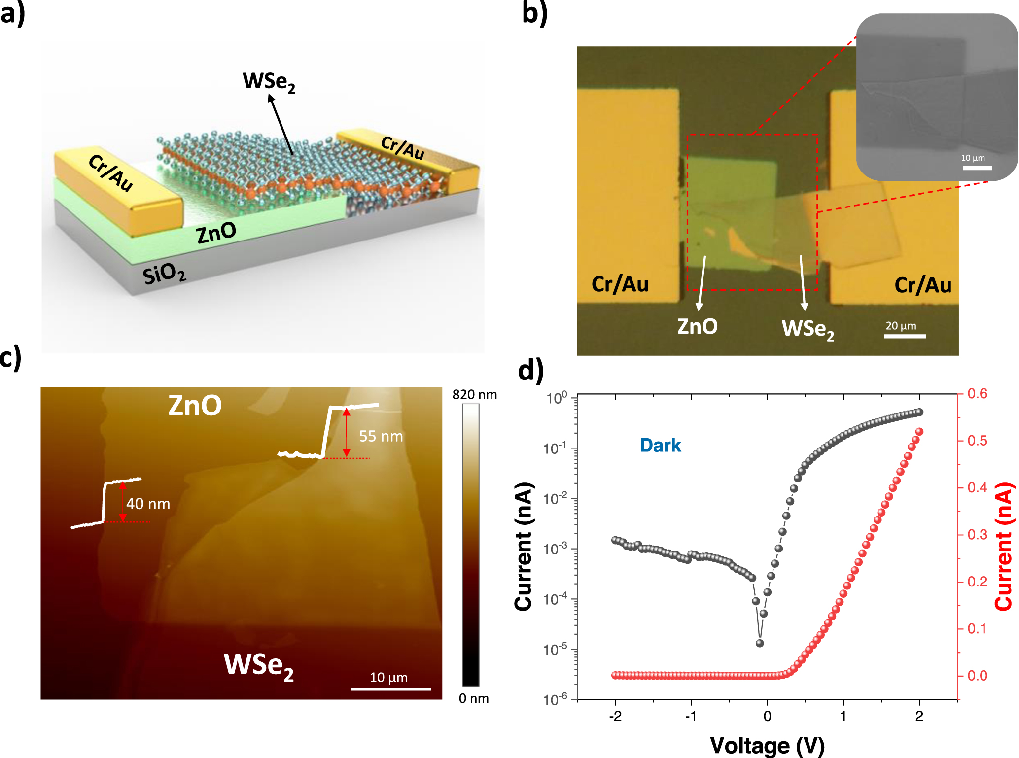
A p-type WSe2 crystal was transferred on the square shaped 40 nm thick n-type ZnO thin film. Two Cr/Au metal electrode contacts were deposited, one on the ZnO thin film and the other on the 2D WSe2. Figure 1(a) shows the schematic illustration of the WSe2/ZnO heterostructure on the SiO2/Si substrate and the optical image of the fabricated WSe2/ZnO heterostructure is shown in figure 1(b). The contact area between WSe2 and ZnO was calculated to be ∼637 μm2. The scanning electron microscopy (SEM) image of the junction is also shown in the inset of figure 1(b). The energy dispersive x-ray spectroscopy was performed to confirm the elemental composition of ZnO and WSe2 materials (figure S2). The thickness of multilayer WSe2 flake and ZnO thin film are ∼55 nm and ∼40 nm, respectively, as determined by atomic force microscopy (AFM) (figure 1(c)). Monolayer WSe2 has a direct bandgap, which makes it attractive for optoelectronic applications, but its low thickness hinders light absorption [33, 34]. In contrast, although multilayer WSe2 has an indirect bandgap, the larger thickness can lead to high optical absorption with values approaching unity when coupled with a back reflector, making it suitable for photodetection applications [35]. The current–voltage (I–V) characteristic of the WSe2/ZnO heterojunction under dark condition is illustrated in figure 1(d), showing a high current rectification ratio, defined as the ratio of current at ±1 V, of ∼103 without gate bias voltage. The diode rectification behavior can be attributed to the built-in electric field at the WSe2/ZnO interface [36]. Note that the Cr/Au electrode connected to the ZnO thin film is grounded during the I–V measurements.

Figure 1. Structural and electrical characterization of the WSe2/ZnO heterostructure. (a) Schematic illustration of the WSe2/ZnO heterostructure device. (b) Optical microscopy image of the WSe2/ZnO heterostructure. The inset shows the SEM image of the WSe2/ZnO heterostructure. (c) AFM image of the WSe2/ZnO heterostructure, shows that the thickness of WSe2 and ZnO are ∼55 nm and ∼40 nm, respectively. (d) The I–V characteristics of the WSe2/ZnO heterostructure under dark condition in the logarithmic (black) and linear (red) scales, show a current rectification of ∼103 without a bias voltage.
Download figure:
Standard image High-resolution imageThe strong optical absorption of WSe2 [37] in the visible-near-infrared ranges and ZnO at UV range [38] and the diode rectifying nature of the WSe2/ZnO heterojunction device makes it suitable for photodetection applications. The I–V characteristics of the WSe2/ZnO heterostructure device under dark and light illumination are demonstrated in figure 2(a). The current increases about four orders of magnitude upon light illumination at zero bias voltage (figure 2(a)) [4]. The self-powered collection of the photo-generated carriers at zero bias could be attributed to the strong built-in electric field at the WSe2/ZnO interface and the photovoltaic effect [39]. The inset of figure 2(a) shows the schematic illustration of the WSe2/ZnO heterojunction under light illumination. In figure 2(a), the photocurrent of ∼0.01 μA at the light intensity of 1.5 mW cm−2 and the device area of S = 3480 μm2, corresponds to a photocurrent density of ∼300 μA cm–2 for this device, which is relatively high compared to the previously reported 2D materials-based photodetectors [40, 41]. The small offset in the I–V characteristic at zero voltage may be due to the adsorption of oxygen and water molecules on the device surface [42, 43] or the existence of a parasitic capacitance in parallel with the device resistance [44]. Nevertheless, this deviation does not affect the performance of the device since the current–time (I–t) measurements show a constant dark current of ∼22 fA without deviation. Figure S3 shows that the open-circuit voltage (Voc) and short-circuit current (Isc) of the WSe2/ZnO heterojunction device becomes as high as 350 mV and 15.6 nA, respectively, under UV light (λ = 365 nm) illumination at a light intensity of 4.58 mW cm−2. A high Iphoto/Idark ratio of 105 was also measured using a light intensity of 4.58 mW cm−2, which is higher than that of previously reported WSe2-based heterojunctions [45, 46].

Figure 2. Self-powered photodetector characterization of the WSe2/ZnO heterojunction. (a) The I–V characteristics of the WSe2/ZnO heterojunction device under dark and light illumination (λ = 470 nm). Inset shows the device schematic under light illumination. (b) The I–t characteristics of the WSe2/ZnO heterojunction over a wide range of wavelengths (λ = 300–850 nm) at the same light intensity of 42 μW cm−2 and zero bias voltage. (c) The responsivity and EQE over a wide range of wavelengths (λ = 300–850 nm) at the same light intensity of 42 μW cm−2 and zero bias voltage. (d) The I–t characteristics of the WSe2/ZnO heterojunction over different light intensities (2–42 μW cm−2) at the wavelength of λ = 300 nm and zero bias voltage. (e) The photocurrent amplitude at different light intensities (2–42 μW cm−2). (f) The responsivity and detectivity of the WSe2/ZnO heterojunction as a function of light intensity (2–42 μW cm−2).
Download figure:
Standard image High-resolution imageTo evaluate the self-powered photodetection performance of the WSe2/ZnO device, the dynamic current–time (I–t) characteristics of the device was measured under monochromatic light illumination at different wavelengths ranging from λ = 300 to 850 nm, each with the same light intensity of 42 μW cm–2, under zero bias voltage (figure 2(b)). The highest photocurrent of ∼12 pA is achieved at λ = 300 nm, which is in agreement with the light absorption spectrum of WSe2 and ZnO [37, 38]. The photoresponsivity and external quantum efficiency (EQE) of the WSe2/ZnO device under illumination over a wide range wavelength of λ = 300–850 nm are shown in figure 2(c). The maximum and minimum responsivities of 45 and 0.67 mA W−1 are obtained at λ = 300 nm and 850 nm, respectively. Also, this photodetector has a responsivity of 17 mA W−1, 6.54 mA W−1, and 1.12 mA W−1 at the wavelengths of 700, 750, and 800 nm. Despite its low responsivities in the 700–850 nm range, it is still classified as a broadband detector due to its ability to detect light across the UV (300–380 nm), visible (380–700 nm), and NIR (700–850 nm) spectra [4, 47]. The maximum EQE of ∼18% was also achieved at λ = 300 nm at the light intensity of 42 μW cm–2. The I–t characteristics of the WSe2/ZnO device at λ = 300 nm over several light intensities of ∼2 to ∼42 μW cm–2 at zero bias are illustrated in figure 2(d). With increasing light intensity from 2 to 42 μW cm−2, the photocurrent amplitude increases linearly (figure 2(e)), which is consistent with earlier findings [9, 10]. The photoresponsivity (R) and detectivity (D*) of the WSe2/ZnO heterojunction versus light intensity at λ = 300 nm are shown in figure 2(f). Both responsivity and detectivity decrease as the light intensity increases which may be due to higher carrier recombination at higher light intensities [10]. The maximum photoresponsivity and detectivity are ∼131 mA W−1 and ∼3.92 × 10¹⁰ Jones at the wavelength of λ = 300 nm with a light intensity of ∼2 μW cm−2 at zero bias. The EQE was also calculated to be ∼54.3% at the lowest light intensity of ∼2 μW cm−2, which is much higher than the EQE of ∼18% at the highest light intensity of ∼42 μW cm−2. The observation of the higher EQE at low incident light intensity than at high light intensity has also been shown in WSe2 photodetectors [48]. The peak in responsivity and EQE at λ = ∼700 nm could be attributed to the excitonic absorption peak in WSe2 [49, 50]. The dark current of this photodetector device is also remarkably low, ∼22 fA, which may be suppressed by the depletion region at the WSe2/ZnO interface [51]. The main photodetector parameters including responsivity (R), detectivity (D*), and EQE values were calculated using the equations (1)–(4) [52, 53].


where Iph, Idark, and Ilight are the photocurrent, dark current and current under illumination, respectively; P is the light intensity and S is the effective surface area and h, c, e, and λ are Planck's constant, speed of light, electron charge constant, and wavelength, respectively [52].
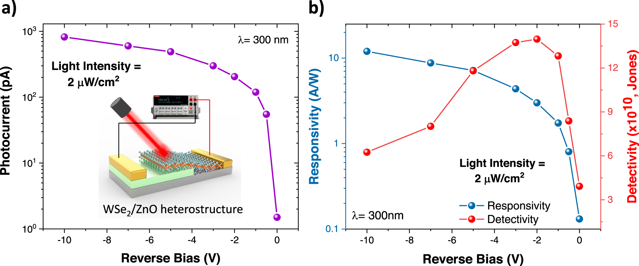
To investigate the collection/separation of photo-generated carriers under different reverse voltage conditions, the photocurrent was measured under several reverse bias voltages at a constant light intensity of 2 μW cm−2 and the wavelength of λ = 300 nm. Figure 3(a) shows the amplitude of the generated photocurrent under reverse bias voltages of 0, −0.5, −1, −2, −3, −5, −7, and −10 V. A schematic illustration of the measurement setup is shown in the inset of figure 3(a). Small reverse bias voltages (e.g. −0.5 V and −1 V) result in a significant increase in photocurrent due to the facilitation of charge collection. The effect of reverse bias on photocurrent nearly saturates at values ≥ −5 V (figure 3(a)) [4, 54]. The maximum photoresponsivity of 11.98 A W−1 was obtained at the voltage bias of −10 V (figure 3(b)). Note that both dark current and photocurrent increase with increasing reverse bias voltage (figure S4). The responsivities of 1.74, 2.99, 4.37, 7.16, and 8.77 A W−1 were achieved for the reverse biases of −1, −2, −3, −5, and −7 V, respectively (figure 3(b)), which are much higher than the responsivity at the zero bias (0.131 A W−1). Interestingly, as the applied reverse bias voltage across the WSe2/ZnO heterojunction increases, the responsivity increases sublinearly but the detectivity increases up to the peak value of ∼1.39 × 10¹¹ Jones at −2 V and thereafter decreases with further increase in applied reverse bias voltage [55]. The detectivity highly depends on the responsivity and the dark current of the device (equation (4)). At the bias voltages higher than −2 V, the dark current increase rate is surpassing the responsivity growth rate, resulting in a decrease in detectivity. Therefore, the optimum performance of the WSe2/ZnO photodetector is at a reverse bias voltage of −2 V. The EQE of the device increases significantly to a value of ∼4958% at the bias voltage of −10 V (figure S5). The EQE cannot exceed 100% at zero bias without photomultiplication [4]. With the help of the reverse bias, the EQEs can enhance to values much higher than 100% due to the photoconductivity gain effect [4]. Note that the whole device area (S = 3480 μm2) is considered active for the calculation of the responsivities/detectivities at the non-zero bias voltages.

Figure 3. Photodetector characterization of the WSe2/ZnO heterojunction at several reverse bias voltages. (a) The photocurrent of the WSe2/ZnO heterojunction at several reverse bias voltages with the same light intensity of 2 μW cm−2 and λ = 300 nm. Inset illustrates the schematic of the device under illumination at a reverse bias voltage. (b) The responsivity (R) and detectivity (D*) of the photodetector at several reverse bias voltages with the same light intensity of 2 μW cm−2 and λ = 300 nm.
Download figure:
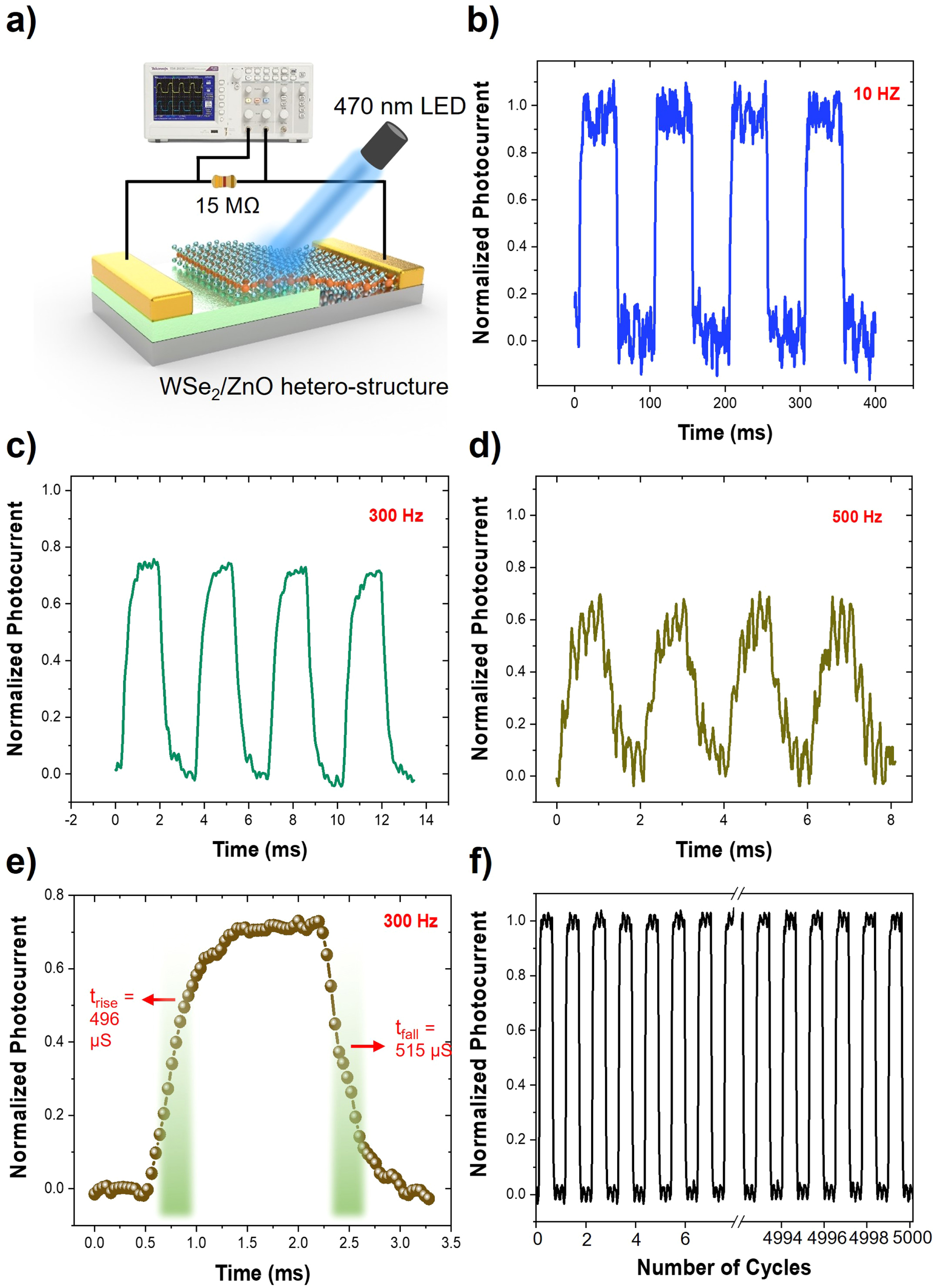
Standard image High-resolution imageThe self-powered frequency-dependent photoresponse of the WSe2/ZnO photodetector was investigated in figure 4. A 470 nm LED powered by a function generator was used to generate light pulses with different frequencies and the WSe2/ZnO device was connected to an oscilloscope through a resistor (15 MΩ) to measure the time-dependent photocurrent (figure 4(a)). The normalized I–t characteristics of the device with zero applied voltage under the light frequencies of 10, 300, and 500 Hz are shown in figure (b)–(d), respectively. The normalized photoresponses in frequencies of 50, 150, and 800 Hz are also illustrated in figures S6(a)–(c). The photocurrent amplitude as a function of light frequency is shown in figure S6(d), illustrating a cut-off frequency of ∼300 Hz. The amplitude of the photoresponse at 300 Hz is about ∼0.74 which is about 70% of its maximum value at the frequency of 1 Hz. At higher frequencies, the photocurrent amplitude drops significantly. The cut-off frequency is the frequency at which the amplitude of the photocurrent signal drops by a factor of 70% [4]. The response time and fall times of ∼496 and ∼515 μs were measured for a square wave optical input signal with a frequency of 300 Hz (figure 4(e)), demonstrating the suitability of this device for fast self-powered optoelectronic applications. Figure 4(f) illustrates the stability of the photoresponse of the WSe2/ZnO photodetector over 5000 consecutive light pulses, showing a square wave photoresponse without a notable degradation in the signal amplitude.

Figure 4. The frequency-dependent photoresponse of the WSe2/ZnO heterojunction device. (a) Schematic of the setup for dynamic response measurements. Normalized photocurrent of the WSe2/ZnO device with zero applied voltage under the optical pulses with λ = 470 nm and frequencies of (b) 10 Hz, (c) 300 Hz, and (d) 500 Hz. (e) Single normalized photocurrent signal at the frequency of 300 Hz. The rise and fall times are 496 μs and 515 μs, respectively. (f) The stability test of the WSe2/ZnO device over 5000 consecutive optical pulses (λ = 470 nm) at zero bias voltage.
Download figure:
Standard image High-resolution imageThe photodetection performance of the recently published 2D WSe2- and ZnO-based photodetectors is compared to our WSe2/ZnO heterojunction photodetector in table 1. The WSe2/ZnO heterojunction photodetector is broadband, highly responsive, fast, and offers high responsivities and detectivities, compared to the previous works listed in table 1. The responsivity of the WSe2/ZnO device under reverse bias voltages is almost two orders of magnitudes higher than those of other WSe2- and ZnO-based photodetectors.
Table 1. Performance evaluation of the WSe2/ZnO photodetector in comparison to other WSe2- and ZnO-based photodetectors in terms of the device structure, bias voltage, wavelength (λ), maximum responsivity (Rmax), rise/fall times (trise/tFall), and maximum detectivity (D*max).
| Device structure | Self-powered | λ (nm) | Rmax (mA W–1) | trise | tfall | D*max (Jones) | References |
|---|---|---|---|---|---|---|---|
| WSe2/Graphite | No (1 V) | 390–1080 | 6.66 | 0.8 (S) | 1.4 (S) | 1.98 × 10⁸ | [56] |
| WSe2 monolayer | No (1 V) | 400–1400 | 360 | 310 (mS) | 930 (mS) | 1 × 10⁹ | [57] |
| WSe2/graphene/MoTe2 | Yes (0 V) | 350/1050 | 40.84 | 468 (μS) | 428 (μS) | 1.2 × 10¹¹ | [45] |
| WSe2/MoTe2 | Yes (0 V) | 400–1700 | 1.8 | 72 (μS) | 48 (μS) | — | [46] |
| WSe2/MoSe2 | Yes (0 V) | 375–811 | 100 | 1.25 (mS) | 1.5 (mS) | 5.78 × 10¹⁵ | [58] |
| WSe2/MoSe2 | No (−2 V) | 1550 | 127 | — | [59] | ||
| MoTe2/Si | Yes (0 V) | 400–1550 | 260 | 5 (μS) | 8 (μS) | 2 × 10¹³ | [60] |
| MoS2/Si | Yes (0 V) | 450–1050 | 210 | 3 (μS) | 40 (μS) | 1 × 10¹³ | [61] |
| MoSe2/Si | Yes (0 V) | 405–2500 | 522 | 18 (μS) | 10 (μS) | 6.7 × 10⁹ | [62] |
| ZnO film | No (30 V) | 200–400 | 67.08 | — | — | — | [63] |
| ZnO/Si | No (4 V) | 200–500 | 360 | 11 (S) | 14 (S) | — | [64] |
| ZnO/Se film | Yes (0 V) | 300–600 | 2.65 | 0.69 (mS) | 13.5 (mS) | — | [65] |
| WSe2/ZnO | Yes (0 V) | 131 | 496 (μS) | 515 (μS) | 3.92 × 10¹⁰ | ||
| No (−2 V) | 300–850 | 2995 | 1.39 × 10¹¹ | This Work | |||
| No (−5 V) | 7160 | 1.18 × 10¹¹ | |||||
| No (−10 V) | 11983 | 6.2 × 10¹⁰ |
To investigate the mechanism of the self-powered photodetection in the WSe2/ZnO heterojunction, three devices based on the ZnO thin film, WSe2 crystal, and WSe2/ZnO heterojunction were fabricated. The schematic of the Cr-ZnO-Cr, Cr-WSe2-Cr, and Cr-WSe2/ZnO-Cr structures under light illumination are shown in figures 5(a)–(c), respectively. Figures 5(d)–(f) illustrate the energy band diagram of the devices under light illumination. The electron affinity of ZnO is ∼4.3–4.5 eV [66] and the work function of Cr is ∼4.5 eV [9], resulting in two equal Schottky barriers with the Cr electrodes (figure 5(d)) [67]. These equal Schottky barriers lead to a net photocurrent of about zero (∼5 fA) at zero bias when the device is under light illumination (figure 5(g)) [9, 68]. However, the photocurrent is non-zero when applying a bias voltage to the device due to the separation of carriers by the applied electric field [69]. Similarly, the WSe2 crystal, with an electron affinity of ∼4 eV [70] and a work function of ∼4.8 eV [71], forms two equal Schottky barriers with Cr electrodes (figure 5(e)) [71], which results in a net photocurrent of about zero (∼0.03 pA) when the whole device is under light illumination (figure 5(h)). This small photocurrent could be due to the unwanted WSe2/Cr contact area asymmetry at two electrodes [9, 72]. Therefore, the symmetric metal-semiconductor-metal device structure is not suitable for SSPD application [9]. However, when contacting the WSe2 and ZnO, a built-in electric field is formed at the interface due to the energy band bending, leading to a high current rectification ratio of ∼103 under dark conditions and a large net photocurrent (∼45 pA) under light illumination with zero bias (figure 5(i)). Therefore, the high Voc = ∼400 mV and Isc = ∼45 pA in the WSe2/ZnO heterojunction is attributed to the presence of a strong built-in electric field at the WSe2/ZnO interface and the separation/acceleration of electron/hole carriers by the electric field in the depletion region [73]. The ideality factor (n) and barrier height  of the WSe2/ZnO diode are calculated to be n = ∼2.83 and
  (Section I, Supporting Information), which are comparable to the previously reported ZnO/Si heterostructure diode [74].

Figure 5. Working mechanism of the WSe2/ZnO heterojunction. The schematic of (a) the Cr-ZnO-Cr device, (b) the Cr-WSe2-Cr device, and (c) the WSe2/ZnO heterojunction device. The energy band diagram of (d) the Cr-ZnO-Cr device, (e) the Cr-WSe2-Cr device, and (f) the WSe2/ZnO heterojunction device. The I–V characteristics of (g) the Cr-ZnO-Cr device, (h) the Cr-WSe2-Cr device, and (i) the WSe2/ZnO heterojunction device under dark and light conditions.
Download figure:
Standard image High-resolution image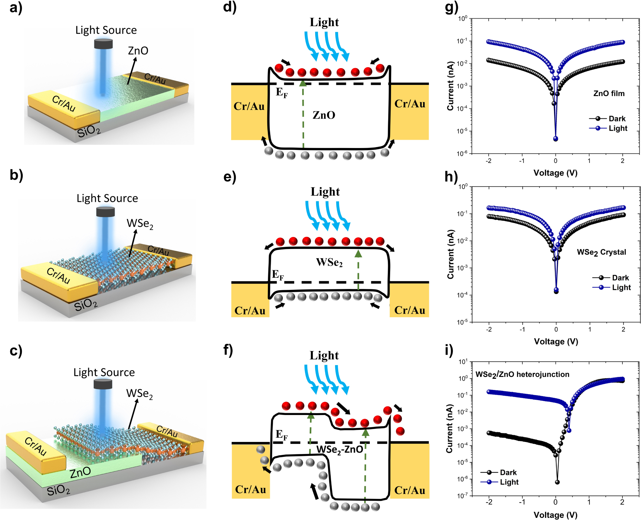
One important consideration for SPPDs is large-area scalability. In this work, the WSe2 flakes were mechanically exfoliated and transferred on the patterned ZnO thin film to demonstrate proof-of-concept WSe2/ZnO photodetection devices. The ZnO thin film is scalable to large areas by ALD and large area 2D materials can be prepared by chemical vapor deposition (CVD) [75] or wet chemical processes [76]. Therefore, it is possible to scale up this proof-of-concept photodetector to an imaging array of WSe2/ZnO photodetectors on a chip. Hence, the fast response, broadband detection, high-speed, and high responsivity of the WSe2/ZnO heterostructure make it an excellent candidate for self-powered optoelectronic applications.
4. Conclusion
A self-powered broadband photodetector based on p-WSe2 and n-ZnO thin film was developed. The WSe2/ZnO p–n heterojunction photodetector showed a broadband response (300–850 nm) with maximum responsivity and detectivity of ∼131 mA W−1 and ∼3.92 × 10¹⁰ Jones under λ = 300 nm at zero bias, respectively. The responsivity and detectivity of the device increase to ∼7160 mA W−1 and ∼1.18 × 10¹¹ Jones, respectively, under a reverse bias voltage of −5 V, which is due to the facilitation of charge collection under bias voltage. The photodetector also exhibited a cut-off frequency of ∼300 Hz, a fast response time of ∼496 μs, and a remarkable photocurrent stability over 5000 light pulse cycles. Hence, the p-WSe2/n-ZnO based photodetector is a candidate for self-powered, high-speed, and broadband photodetection technology.
Acknowledgments
This work was supported by the Natural Sciences and Engineering Research Council of Canada (NSERC), Canada Foundation for Innovation (CFI), British Columbia Knowledge Development Fund (BCKDF), Western Economic Diversification Canada (WD), and Simon Fraser University. The authors thank B Kim for maintenance of the SFU Engineering Science cleanroom facility. The authors acknowledge CMC Microsystems and 4D LABS shared facilities that facilitated this research.
Data availability statement
The data cannot be made publicly available upon publication because they are not available in a format that is sufficiently accessible or reusable by other researchers. The data that support the findings of this study are available upon reasonable request from the authors.
Supplementary data (0.7 MB PDF)