

Abstract
High-performance ultraviolet (UV) detectors with both high responses and fast speeds are hard to make on homogeneous crystal semiconductor materials. Here, the UV response characteristics of mixed-phase MgZnO thin films with different internal structure distributions are studied. The mixed-phase MgZnO-based detector with the given crystal composition has a high response at both deep UV light (96 A W−1 at 240 nm) and near UV light (80 A W−1 at 335 nm). Meanwhile, because of the quasi-tunneling breakdown mechanism within the device, the high-response UV detector also shows a fast response speed (tr = 0.11 μs) and recovery speed (td1 = 26 μs) at deep UV light, which is much faster than both low-response mixed-phase MgZnO-based UV detectors with other structure constitutions and reported high-response UV devices on homogenous crystal materials. The Idark of the device is just 4.27 pA under a 5 V bias voltage, so the signal-to-noise ratio of the device reached 23852 at 5.5 uW cm−2 235 nm UV light. The new quasi-tunneling breakdown mechanism is observed in some mixed-phase MgZnO thin films that contain both c-MgZnO and h-MgZnO parts, which introduce a high response, signal-to-noise ratio, and fast speed into mixed-phase MgZnO-based UV detectors at weak deep UV light.
Export citation and abstract BibTeX RIS
1. Introduction
The study of ultraviolet (UV) detectors has become one of the main directions of photoelectron technology, which is mainly attributed to the development of multiple related application areas, such as ultrahigh-speed UV communication, large capacity information storage, threat detection, flame and missile plume alarms, and UV environmental surveillance [1–6]. The aim is to achieve effective and fast detection at deep UV (l < 280 nm) and near UV light (300 nm < λ < 400 nm), a wide band gap material with a high response, low dark current, and fast speed which are needed in high-performance UV detectors. During the past 10 years, high-response deep UV (λ < 280 nm) detectors have been made on multiple types of wide band gap materials with a homogeneous crystal structure, such as AlGaN, SnO2, MgxZn1−xO, β-Ga2O3, and so on [7–10]. The response of single crystal β-Ga2O3 reached 1000 A W−1 at 240 nm deep UV light [11], and the response of hexagonal MgxZn1−xO thin film reached 1.8 × 10⁴ A W−1 at 276 nm deep UV light [12, 13]. In addition, theoretically, MgxZn1−xO is sensitive at UV light ranged widely from 160 nm–380 nm [14–27], and our group has made cubic structure MgZnO thin films that could detect UV light between 220 nm and 348 nm [28–31], which makes MgZnO an ideal material in high-performance detectors at both near UV light (300 nm < λ < 380 nm) and deep UV light (200 nm < λ < 300 nm). The high UV responses of single structure materials with a simple metal–semiconductor–metal (MSM) structure, such as AlGaN, SnO2, MgxZn1−xO, β-Ga2O3, and so on, are caused by the good collection ability of the materials as photogenerated carriers and the hole-trapping mechanism in the homogenous structure materials-based device [13]. Unfortunately, there are two inevitable problems in homogeneous crystal materials-based UV detectors in their actual response ability at faint deep UV light. Firstly, the good collection ability of the homogeneous crystal materials works as carriers under both dark and deep UV conditions, so the high UV response and high Idark level would exist in homogeneous crystal material-based UV detectors simultaneously, and the signal-to-noise ratios of the devices are usually small. The Idark of the high-response hexagonal MgxZn1−xO-based detector is 20 mA, so the signal-to-noise ratio of the device is just 2.25 [12]. Because deep UV light would experience intense attenuation during its transfer process in air, the intensity of deep UV light is much weaker than infrared (IR) and visible light signals on the surface of the Earth. Therefore, this high dark current and low signal-to-noise ratio of the UV detector is far below the level that is needed in effective detection at faint deep UV light under strong noise background on Earth, as shown in figure 1(a). Secondly, the high UV response of the homogeneous crystal material-based UV detectors is caused by the hole-trapping mechanism, which would induce a slow decay speed inevitably from both theory and experimental results. Several seconds or minutes is often needed for the recovery process of the high-response UV detectors based on homogeneous crystal materials with the UV off, as shown in figure 1(b). Therefore, when homogeneous crystal material is used in a solar-blind UV detector, high response, high signal-to-noise ratio, and fast decay speed could not exist in one detector simultaneously.
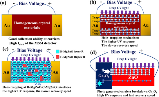
Figure 1. (a) Schematic image of the MSM structure detector on homogeneous crystal materials. (b) Hole-trapping mechanism in the high-response MSM structure UV detector on homogeneous crystal materials. (c) Hole-trapping mechanism in the high-response MSM structure detector on mixed-phase MgZnO thin film. (d) Breakdown mechanism in the Ga2O3/ZnO heterojunction UV detector.
Download figure:
Standard image High-resolution imageRecently, high-response deep UV detectors with both h-MgxZn1−xO and c-MgxZn1−xO have been reported. The signal-to-noise ratio of the mixed-phase MgZnO-based detector under deep UV (240 nm) light is much higher than single structure materials [15–17, 19, 27]. Therefore, mixed-phase MgxZn1−xO thin films are even better materials in high-performance UV detectors at both near UV (300 nm–380 nm) and deep UV (220 nm–280 nm) light. The high UV response of mixed-phase MgZnO-based detectors has also been interpreted by the hole-trapping mechanism at the c-MgZnO/h-MgZnO interfaces, but the recovery speed of the MgZnO UV detector is usually slow because of the self-contradiction in the hole-trapping mechanism, as shown in figure 1(c). The P type-Insulation-N type (P-I-N) structure IR detector is a commonly used detector type in high-performance devices; high response, high signal-to-noise ratio, and fast decay speed exist simultaneously in one device because of the avalanche breakdown mechanism. In the design of the avalanche breakdown diode device, the introduction of both the low resistance semiconductor layer and the high resistance insulator are key factors. Recently, several reports have shown that mixed-structure material-based detectors, such as Ga2O3/ZnO, graphene/PbS quantum dot, graphene/CH3NH3PbBr2I, and TiO2-ZnTiO3 detectors with different resistance layers have shown ultrahigh responses to visible or UV light [32–36]. The high UV response of Ga2O3/ZnO structure detectors have been reported to be caused by the avalanche breakdown effect, as shown in figure 1(d). Mixed-phase MgZnO thin film is constituted alternatively by high resistance c-MgZnO and low resistance h-MgZnO, which is near the situation in the Ga2O3/ZnO system. Therefore, a similar breakdown phenomenon may occur at c-MgZnO/h-MgZnO interfaces in the mixed-phase MgZnO thin film, which would introduce both high UV response and fast recovery speed of the mixed-phase MgZnO-based detector. Through systematic study of the UV response characteristics of mixed-phase MgZnO thin film with a structure constitution gradually changing between a cubic and hexagonal structure, a mixed-phase MgZnO thin film with better performance in UV detection can hopefully be developed. If the breakdown phenomenon indeed exists in mixed-phase MgZnO thin film, the internal gain and UV response of mixed-phase MgZnO would be much higher, and the contradiction between the high UV response and fast recovery speed would hopefully be eliminated. Thus, a study on the breakdown mechanisms in mixed-phase MgZnO thin films with different microstructure distributions is not only meaningful in developing an ideal material for effective and fast detection at faint deep UV light, but also beneficial for developing a simple UV-sensitive material free from slow response and recovery speeds at deep UV light.
The present authors have studied the properties of MgZnO thin films grown using the pulsed laser deposition (PLD) method under different oxygen pressures and temperature conditions. Just a small change in the structure of the MgZnO thin films appears when oxygen pressure and temperature are changed separately. If the oxygen pressure and temperature are simultaneously changed, the structure of the MgZnO thin films will change greatly, which is beneficial for research on the performance of MgZnO thin films in UV detection, with the structure changed gradually between a cubic and hexagonal structure. A systematic study on the UV response characteristics of mixed-phase MgZnO-based UV detectors with different structure constitutions could then be conducted.
In this paper, MgZnO thin films with a gradient change in crystal structure (from cubic to hexagonal) were produced under different oxygen pressures and temperatures using the PLD method. The different performances in UV detection of the mixed-phase MgZnO thin films were then measured, and the mechanisms of the performance of the MgZnO UV detectors with different structure constitutions were studied.
Table 1. Detailed deposition conditions of the MgZnO thin films on a fused quartz substrate.
| Condition number | Temperature (°C) | Oxygen pressure (Pa) | Oxygen flow rate (SCCM) |
|---|---|---|---|
| 1 | 300 | 3.0 | 17.6 |
| 2 | 350 | 3.5 | 20.0 |
| 3 | 400 | 4.0 | 27.4 |
| 4 | 450 | 4.5 | 33.7 |
| 5 | 500 | 5.0 | 40.0 |
| 6 | 600 | 6.0 | 50.0 |
| 7 | 650 | 7.0 | 50.0 |
2. Experimental section
2.1. Growth of the MgZnO thin films
The MgZnO thin films were deposited on fused quartz using the PLD method. Before the deposition of the MgZnO thin film, the background pressure in the chamber was pumped down a high vacuum (10−6 Torr) level. During the growth process, a KrF (248 nm and 520 ns) pulsed laser with a 30 J cm−2 laser energy density was added on a Mg0.3Zn0.7O target. The deposition temperature was gradually increased from 300°C to 650°C, while the oxygen pressure was also gradually increased simultaneously from 3 Pa to 7 Pa through the modulation of the oxygen flow rate into the chamber, as shown in table 1. The MgZnO thin films would have deposited more along one structure on the crystal substrate, and both cubic and hexagonal structure MgZnO would exist on quartz substrate, which has been found out in our previous studies [19, 29, 30, 37, 38]. A fused quartz substrate was chosen to fabricate the mixed-phase MgZnO with an obviously different structure constitution.
2.2. Structural and UV absorption analysis
The crystal structures of the MgZnO thin films were investigated by a D/max-RA x-ray diffractometer. The UV absorption characteristics of the MgZnO thin films were measured by a Shimadzu UV-2450PC scanning spectrophotometer. The influence of the glass was eliminated during the testing procedure, and just an error smaller than 3% exists in the measurement process.
2.3. UV response characteristics
The UV response characteristics of the MgZnO UV detectors were found using a 200 W UV-enhanced Xe lamp and a monochromator. The electric properties of the MgZnO detectors under both dark and UV conditions were measured by a semiconductor parameter analyzer (Keithley 4200).
3. Results and discussion
Figure 2(a) shows the x-ray diffraction (XRD) spectrums that show the crystal structure of the MgZnO thin films deposited under different conditions, where each pattern is measured and confirmed multiple times. The detailed conditions of each MgZnO thin film are listed in table 2. In the XRD patterns of the MgZnO thin films deposited under different conditions, XRD peaks corresponding to both hexagonal MgZnO (h-MgZnO) and cubic MgZnO (c-MgZnO) appear. In the XRD pattern of the MgZnO thin film deposited at the lowest temperature, oxygen pressure, and oxygen flow rate conditions, the XRD peaks corresponding to c-MgZnO are much stronger than the ones corresponding to h-MgZnO. In the XRD pattern of the MgZnO thin films deposited at higher temperature, oxygen pressure, and oxygen flow rate conditions, the XRD peaks corresponding to c-MgZnO generally become weaker, and the XRD peaks corresponding to h-MgZnO generally become stronger. Abnormal results are observed for the samples when the deposition conditions are changed from condition 2 to condition 3 and from condition 6 to condition 7. The relative Mg and Zn contents of the MgZnO thin films deposited under different conditions are measured by Energy Dispersive Spectrometer (EDS), as shown in figure 2(b), where the total Mg and Zn atom content is set as 100%. As seen from this figure, the relative Mg composition in the MgZnO thin films increases when the deposition temperature, oxygen pressure, and flow rate increase simultaneously, and a dramatic increase in the Mg content of the MgZnO thin films occurs when the deposition temperature, oxygen pressure, and flow rate are increased to high values.
Table 2. Comparison of the main parameters between our mixed-phase MgZnO UV detector and reported results.
| Decay time | ||||||||
|---|---|---|---|---|---|---|---|---|
| Material | Device type | Responsivity | Idark | Iuv/Idark | trise | t1 | t2 | References |
| Mixed-phase MgZnO | MSM | 96 A W−1 (240 nm) | 4.27 pA (5 V) | 23852 (5 V) | 0.11 us | 26 us | 0.53 ms | This work |
| Mixed-phase MgZnO | MSM | 8.895 (260 nm) | 8.29 pA (40 V) | 103 (10 V) | — | 1–2 s | [15] | |
| h-MgZnO | MSM | 1.8 × 10⁴ A W−1 (276 nm) | 20 mA (10 V) | 2.25 (10 V) | 5.7 ms | 35.3 ms | [12] | |
| β-Ga2O3 | MSM | 259 A W−1 (235 nm) | 40 pA (20 V) | 104 (20 V) | — | — | [9] | |
| β-Ga2O3 | MSM | 1000 A W−1 (240 nm) | 1 nA (20 V) | 103 (20 V) | — | — | [11] | |
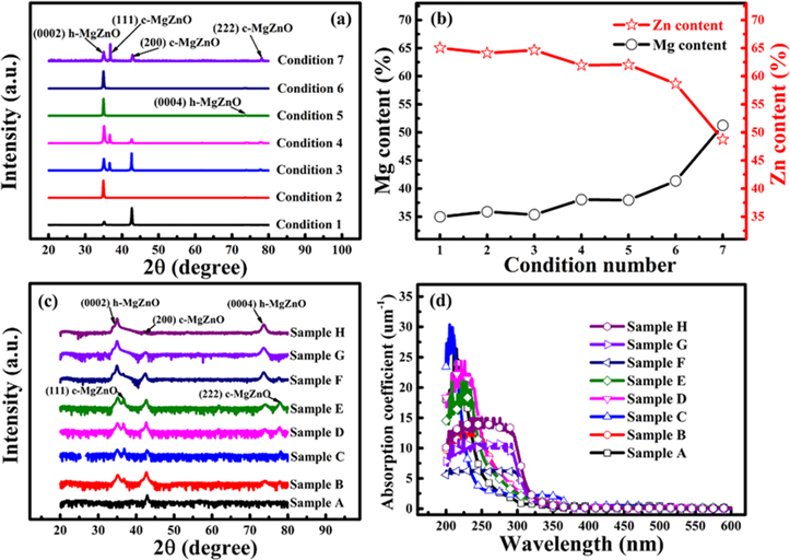
Figure 2. (a) XRD patterns of MgZnO thin films deposited on a fused quartz substrate under different conditions. (b) The relative Mg and Zn compositions of the MgZnO thin films deposited under different condition measured by EDS. (c) XRD spectrums of the MgZnO thin films with gradual structural changes between a cubic and hexagonal structure. (d) UV absorption spectrums of the MgZnO thin films with different structures.
Download figure:
Standard image High-resolution imageAccording to previous results, because of the change in the atomic distribution on the surface of the substrate, more hexagonal MgZnO and less cubic MgZnO appear in the high-temperature deposited MgZnO thin films. When the oxygen pressure increased, because the migration energies of the Mg, Zn, and O atoms decreased, more h-MgZnO and less c-MgZnO appeared in the mixed-phase MgZnO thin films [28, 37, 38]. Therefore, generally, more h-MgZnO and less c-MgZnO appeared in the mixed-phase MgZnO thin films when the temperature and oxygen pressure increased simultaneously. But the Mg composition in the MgZnO thin films is higher under higher temperatures, oxygen pressure, and flow rate conditions. The increase in the Mg composition sometimes has a stronger impact than the deposition conditions. Thus, more c-MgZnO and less h-MgZnO appears in the MgZnO thin films when the deposition condition is changed from condition 2 to condition 3, and a similar change appears in the samples when the condition changes from condition 6 to condition 7.
From the above results, mixed-phase MgZnO thin films with dramatic changes between hexagonal and cubic structures are produced under different conditions, but the cubic structure MgZnO is hard to make with the Mg0.3Zn0.7O target. To realize the effect of the change in the structure of the MgZnO thin films on their UV response characteristics, a c-MgZnO thin film was produced with the Mg0.4Zn0.6O target under condition 1, and the XRD spectrums of the MgZnO thin films with gradual structural changes between the cubic and hexagonal structure, named A to H, are rearranged, as shown in figure 2(c). Figure 2(d) shows the UV absorption characteristics of the MgZnO thin films with different structure constitutions. Only one UV absorption edge, located at approximately 250 nm, is observed in the UV absorption spectrums of the c-MgZnO thin film, and one near the UV absorption edge is also observed in the UV absorption spectrum of the MgZnO thin film constituted mainly by h-MgZnO. In contrast, in the UV absorption spectrum of the mixed-phase MgZnO thin film, two edges that are located at both the deep UV and near UV wavelengths appeared, and the near UV absorption edge has a greater impact on the UV absorption characteristics of the mixed-phase MgZnO thin films with more h-MgZnO. In addition, there is much less c-MgZnO in sample F than that in sample E, so the UV absorption edge of sample F is located near the UV position, which is very different from that of sample E.
MSM structure devices were fabricated on the MgZnO thin films with different structure constitutions. Twelve pairs of Au (50 nm thick) finger-type electrodes were made using the lithography and wet etching method, where each Au finger was 500 μm long and 10 μm wide, and a 10 μm space was set between each Au finger, as shown in figure 3(a). The Scanning Electronic Microscopy (SEM ) image of the Au finger type electrodes is shown in figure 3(b). The UV response spectrums of the MgZnO-based UV detectors under a 25 V bias voltage are shown in figures 4(a)–(h). According to this figure, the UV response spectrums of all the MgZnO photodetectors show two peaks between 200 nm and 400 nm. The peak at the shorter wavelength position (deep UV response peak) corresponds to the contribution of c-MgZnO with a higher Mg content, and the peak at the longer wavelength position (near the UV response peak) corresponds to h-MgZnO with a lower Mg content. Therefore, although the MgZnO thin film deposited by the Mg0.4Zn0.6O target shows a cubic structure from the XRD results, there is also a small amount of h-MgZnO distributed sparsely in the sample. In contrast to the peak response of the mixed-phase MgZnO-based detector at deep UV light, the relative peak response of the device at the near UV peak does not directly increase with the relative amount of h-MgZnO in the MgZnO thin film. The near UV response peak of device B is higher than its deep UV response peak; the relative amount of h-MgZnO in device C is higher than that in device B, but the peak response of device C at near UV light is, on the contrary, lower than its deep UV response peak. Compared with device F, more h-MgZnO appeared in device G. Strangely, the near UV response peak of device G was much lower than its deep UV response peak. These two situations obeyed the results that the mixed-phase MgZnO UV detector should be more sensitive at near UV light with more h-MgZnO. In addition, the maximum response of device G reached 4.96 A W−1 at 240 nm UV light under a 25 V bias voltage, and the maximum response of device C reached 1.49 A W−1 at 260 nm UV light with a 25 V work voltage. Although great differences exist in the structural compositions of the two MgZnO thin films within these two devices, both devices showed a higher response at deep UV light, and the deep UV responses of the two devices are much higher than those of the other devices. Insets in figures 4(a)–(h) show the UV response spectrums of each device with a work voltage ranging from 5 V to 25 V. The two peak responses of each device at both the near and deep UV positions increase with the bias voltage.

Figure 3. (a) Schematic image of the MSM structure MgZnO UV detector. (b) SEM image of the Au electrode in the devices.
Download figure:
Standard image High-resolution image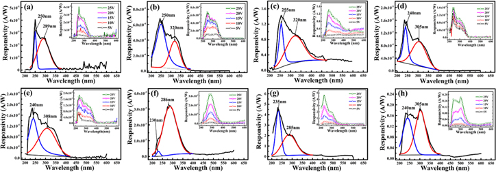
Figure 4. UV response spectrums of the UV detectors based on MgZnO thin films with different structure constitutions. (a) Device A on sample A. (b) Device B on sample B. (c) Device C on sample C. (d) Device D on sample D. (e) Device E on sample E. (f) Device F on sample F.
Download figure:
Standard image High-resolution imageFigures 5(a)–(h) show the the Idark, Iuv, and Iuv/Idark ratio of the MgZnO UV detectors with different structural constitutions. The dark currents (Idark) of devices D and E are 8.35 pA and 15.22 pA under a 25 V bias voltage, which are much lower than those of the other devices. The dark currents (Idark) of devices C and G with higher UV responses are 2.32 uA and 1.24 uA under a 25 V bias voltage, which are much higher than those of the other devices.
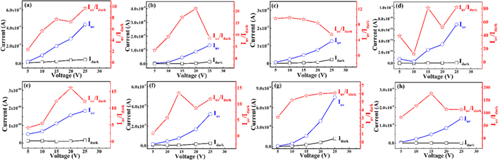
Figure 5. The Idark, Iuv, and Iuv/Idark ratio of the UV detectors based on MgZnO thin films with different structure constitutions. (a) Device A on sample A. (b) Device B on sample B. (c) Device C on sample C. (d) Device D on sample D. (e) Device E on sample E. (f) Device F on sample F.
Download figure:
Standard image High-resolution imageThe time response spectrums of the MgZnO UV detectors with different structural constitutions are shown in figures 6(a)–(h), which were measured under a deep UV (DUV) pulse laser (l ¼ 266 nm) with a pulse width of 30 ns. In this figure, the rise times (tr : the time interval for the signal of the device to increase from 0% to 63%) of devices C and G with higher UV responses are 0.28 us and 0.18 us, respectively, so the response speeds of the two devices are much faster than the other ones with much lower UV responses. The photo response decay curve of each detector was fitted with a biexponential equation with the following expression [39]:


Figure 6. The time response of the UV detectors based on MgZnO thin films with different structure constitutions. (a) Device A on sample A. (b) Device B on sample B. (c) Device C on sample C. (d) Device D on sample D. (e) Device E on sample E. (f) Device F on sample F.
Download figure:
Standard image High-resolution imageIn equation (1), there are three constants, y0, y1, and y2, and two time constants, td1 and td2. For the decay process of the detector, td1 is the fast-response component, and td2 is the slow-response component. For device C, the fall times td1 and td2 are 19.3 us and 0.55 ms, respectively. For device G, the fall times td1 and td2 are 12.3 us and 0.19 ms. The recovery speeds of the two devices are also much faster than those of the other devices with lower UV responses. Mixed-structure materials-based UV detectors (mixed-phase MgZnO and TiO2-ZnTiO3) have shown higher UV responses because of the hole-trapping phenomenon. According to this mechanism, the high UV responses of crystalline semiconductor-based devices are achieved at the expense of slow recovery speeds. However, based on our experimental results, the recovery speeds of the high-response mixed-phase MgZnO-based detectors are much faster than those of detectors with much lower UV responses. Therefore, the mechanisms of the high-response mixed-phase MgZnO-based detectors may be different.
Figures 7(a)–(h) show the conductive atomic force microscopy (C-AFM) results of the MgZnO thin films with different structural constitutions, which were made with the same current range of 1 pA and the same resolution ratio. From this figure it can be seen that both high resistance (dark) and low resistance (bright) areas exist in the MgZnO thin films with obviously different structural constitutions. The surface of the MgZnO thin film deposited with the Mg0.4Zn0.6O target is mainly covered by the dark area, and the small area with a slightly brighter color distributed sparsely in the sample, so the Idark of the MgZnO-based detector is relatively smaller. When the relative amount of h-MgZnO in the MgZnO thin films increases, although the size of the bright area generally increases, the micro distributions of bright and dark areas within the MgZnO thin films change irregularly. The bright and dark regions are much more dispersed with smaller areas in sample D, so higher density of grain boundary between c-MgZnO and h-MgZnO appears within device D. Because the grain boundaries showed relative higher resistance compared with both MgZnO structures, the Idark of the device is much smaller. In sample E, the difference between the bright colors and dark areas is much bigger than the other samples, so the resistance difference between the different MgZnO structure is much larger. Relative higher grain boundaries exist at the c-MgZnO/h-MgZnO interfaces in this sample than in the other samples, so the Idark of device E is much smaller than that of the other devices.
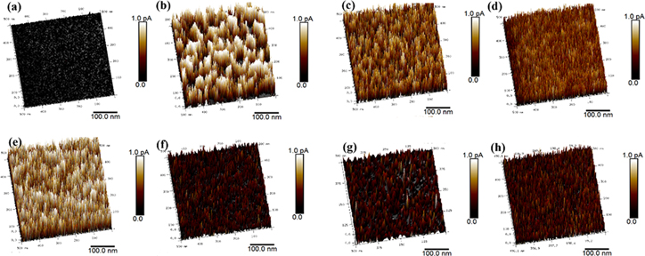
Figure 7. The Conducting atomic force microscope (CFM) images of the MgZnO thin films with different structure constitutions. (a) Sample A. (b) Sample B. (c) Sample C. (d) Sample D. (e) Sample E. (f) Sample F.
Download figure:
Standard image High-resolution imageThe resistance distribution situation in sample C is between that in samples B and D, and the resistance distribution situation in sample G is between that in samples F and H. However, the dark currents (Idark) and light currents (Iuv) of devices C and G are abnormally much higher than those of the other devices. Although the microstructure and resistance distribution of the two MgZnO thin films differ greatly, the dark currents (Idark) and light currents (Iuv) of the two devices are similar. Thus, the Idark and Iuv of the two devices under different voltages cannot be interpreted only by the resistance and microstructure distributions. The dark currents (Idark) and light currents (Iuv) of devices C and G increase dramatically at a higher bias voltage, and the maximum Iuv/Idark ratios of the two devices occur at smaller bias voltages; thus, some kind of breakdown phenomenon may exist in the two devices, which has been seen in the avalanche photodiode detector (APD), the tunnel diode, and the p-n junction. Therefore, an analysis of the high-performance MgZnO UV detector with the given structure constitution should be performed according to the breakdown mechanism within the two mixed-phase MgZnO-based detectors. Two types of breakdown mechanisms, tunneling multiplication and avalanche multiplication, exist in electric devices [40, 41]. A negative temperature coefficient for the breakdown voltage of the device is usually the evidence for the Zener tunneling mechanism, and a positive temperature coefficient for the breakdown voltage of the device is usually the evidence for the avalanche multiplication.
Figure 8 shows the I-V curves of device G at different temperatures. A decreasing breakdown voltage (from 12.1 to 5.15 V) can be observed when the temperature increases from 300 to 400 K, so the quasi-Zener tunneling mechanism is responsible for the high Idark and UV response of the MgZnO UV detector under a higher bias voltage [32]. When deep UV light irradiates the MgZnO UV detector under a relatively high bias voltage, the photogenerated carriers break through the high-resistance c-MgZnO because of the quasi-Zener tunneling phenomenon. Thus, when the deep UV light irradiates the device, the device changes from dark work mode to UV-sensitive work mode, which would be proceeded by the tunneling process of the photogenerated carriers through the high-resistance regions in the device at the higher bias voltage, and the recovery process of the device in the absence of UV light corresponds to the opposite change. Because of the fast switching between these two work modes, which has been observed in Metal-insulator-Semiconductor 'MIS'-structure tunnel junction detectors [42], the response and recovery speeds of device G are faster than the other devices with lower UV responses.
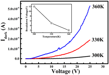
Figure 8. The I-V curve of the high-response MgZnO UV detector (device G) under different temperatures.
Download figure:
Standard image High-resolution imageThe mechanisms for the different UV responses and Idark of the MgZnO UV detectors with different resistance and structure constitutions are shown in figure 9. Both low-resistance h-MgZnO and high-resistance c-MgZnO are distributed alternatively in the MgZnO thin films, as shown in figure 9(a). Because the barriers at the c-MgZnO/h-MgZnO interfaces block the transport of carriers, the Idark of detector D with a higher density of c-MgZnO/h-MgZnO interfaces is much smaller than those of the other devices, and the Idark of the mixed-phase MgZnO detector E with higher barriers at the c-MgZnO/h-MgZnO interfaces is also much smaller, as shown in figures 9(b) and (c) [43]. Device G exhibits a smaller number of high-resistance grain boundaries and less cubic MgZnO between the Au electrodes, and the carriers break down some high-resistance regions (barriers at the c-MgZnO/h-MgZnO interfaces) through the tunneling function at the high bias voltage. Therefore, the Idark of this device is much higher than those of the other devices, and a similar phenomenon appears in device C, as shown in figure 9(d). When deep UV light irradiates device G, many carriers are generated in both h-MgZnO and c-MgZnO; the density of carriers greatly increases in h-MgZnO, and the resistance of both the boundaries between different structure MgZnO phases and c-MgZnO decreases greatly. Both the tunneling probability and the Iuv of device G greatly increase, so the response of the device at deep UV light is much higher than those of the other devices, and a similar phenomenon appears in device C, as shown in figure 9(e). In contrast, when 300 nm near UV light irradiates device G, carriers are generated only in hexagonal MgZnO, and the resistance of the boundaries between different structure MgZnO phases does not decrease as much as that under deep UV conditions. The tunneling probability of photogenerated carriers in device G at 300 nm UV light is much smaller than that of the device under 235 nm deep UV light, so the response of the device at near UV light is lower than the deep UV response of the device, and a similar phenomenon also appears in device C, as shown in figure 9(f). Therefore, although the micro resistance and structure distributions in device C and G are different, the UV responses and dark currents of the two devices are similar because of the similar tunneling breakdown mechanism in the two devices.

Figure 9. Diagram for the mechanism of the UV detector on MgZnO thin film with different resistance parts.
Download figure:
Standard image High-resolution imageFrom our experimental results, the deep UV response of the MgZnO detector constituted by (0002) h-MgZnO and (200) c-MgZnO is higher than those of the other devices because of the quasi-tunneling mechanism. Similar experimental results have been reported in previous studies [15, 16]. However, the Idark of the device is much higher than the previously reported results. Thus, an increase in the amount (200) of c-MgZnO would decrease the Idark of the device because of the high resistance c-MgZnO with more Mg atoms. In addition, because more (200) c-MgZnO may increase the tunneling amplification times of the MgZnO UV detector under deep UV conditions, the deep UV response and the Iuv/Idark ratio of the mixed-phase MgZnO detector with more (200) c-MgZnO would be higher. Under lower oxygen pressure conditions, more (200) c-MgZnO and less h-MgZnO would exist in MgZnO thin film [37, 38]. Thus, a decrease in deposition oxygen pressure is an effective method to induce more (200) c-MgZnO in the MgZnO thin films. The XRD patterns of the MgZnO thin films deposited under oxygen pressures ranging from 3.0 Pa to 3.5 Pa (15 sccm) are shown in figure 10(a). The other conditions are the same as those for sample F. The XRD patterns of sample F, sample G, and sample H, which are constituted by smaller amounts of (200) cubic MgZnO, are also shown in this figure for reference. More (200) c-MgZnO appears in the MgZnO thin films deposited at lower oxygen pressure, and this result agrees with our prediction. The UV absorption spectrums of the MgZnO thin films deposited under oxygen pressures ranging from 3.0 Pa to 3.5 Pa are shown in figure 10(b). The UV absorption edges of the MgZnO thin films with more (200) c-MgZnO makes a blueshift.
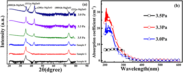
Figure 10. (a) XRD patterns of the MgZnO thin films deposited at lower oxygen pressure. (b) UV absorption spectrums of the MgZnO thin films deposited at higher oxygen pressure.
Download figure:
Standard image High-resolution imageThe UV response spectrums of the three mixed-phase MgZnO detectors under a 25 V bias voltage are shown in figures 11(a)–(c). Two UV peaks appear in the UV response spectrums of the three MgZnO detectors, and a relative bigger difference between the two peak wavelength positions appears in the UV response spectrum of the device deposited at lower oxygen pressure. When the UV detector is made of the mixed-phase MgZnO thin film with slightly more (200) c-MgZnO that is deposited at 3.5 Pa, the maximum response of the detector is just 0.0032 A W−1 at 286 nm deep UV light with a 25 V work voltage, which is close to those of the devices with less (200) c-MgZnO. When the deposition pressure is decreased from 3.5 Pa to 3.3 Pa, much more c-MgZnO appears in the mixed-phase MgZnO thin film. Under a 25 V work voltage, the peak response of the mixed-phase MgZnO-based detector reaches 96 A W−1 at 235 nm deep UV light, which is much bigger than the devices with less (200) c-MgZnO. In addition, the device also shows a high response (80 A W−1) at 335 nm near UV light. However, for the device with even more (200) c-MgZnO at 3.0 Pa, the maximum response is 1.8 A W−1 at 240 nm deep UV light under a 25 V work voltage. This value is much lower than that of the MgZnO detector deposited at 3.3 Pa. From the UV response spectrums of each device with work voltages ranging from 5 V to 25 V (Inserted figures in figures 11(a)–(c)) the two response peaks of each device increase with the bias voltage.

Figure 11. (a) UV response spectrums of UV detectors based on MgZnO thin films deposited at 3.5 Pa. (b) UV response spectrums of UV detectors based on MgZnO thin films deposited at 3.3 Pa. (c) UV response spectrums of UV detectors based on MgZnO thin films deposited at 3.0 Pa. (d) The Idark, Iuv, and Iuv/Idark ratio of the UV detectors based on MgZnO thin films deposited at 3.5 Pa. (e) The Idark, Iuv, and Iuv/Idark ratio of the UV detectors based on MgZnO thin films deposited at 3.3 Pa. (f) The Idark, Iuv, and Iuv/Idark ratio of the UV detectors based on MgZnO thin films deposited at 3.0 Pa. (g) The time response of the UV detectors based on MgZnO thin films deposited at 3.5 Pa. (h) The time response of the UV detectors based on MgZnO thin films deposited at 3.3 Pa. (i) The time response of the UV detectors based on MgZnO thin films deposited at 3.0 Pa.
Download figure:
Standard image High-resolution image
The electrical characteristics and the signal-to-noise ratios of the MgZnO UV detectors with more (200) c-MgZnO are shown in the Idark, Iuv, and Iuv/Idark ratios of the devices, as shown in figures 11(d)–(f). Because much high resistance c-MgZnO decreased much in whole resistance of the device that was deposited at 3.3 Pa, under the 5 V bias voltage, the Idark of the device is only 4.27 pA, and the Iuv/Idark ratio of the device reaches 23852, where the Iuv is measured with 5.5 uW cm−2 235 nm UV light. The signal-to-noise ratio of the device is much higher than those of the other devices with less (200) c-MgZnO, and this value is much higher than the maximum value for a simple MSM structure UV detector with other single-structure materials. In the MgZnO UV detector deposited at 3.0 Pa, even more high resistance (200) c-MgZnO appeared. Therefore, under 25 V bias voltage, the dark current of the device is just 2.07 pA, and the Iuv/Idark ratio of this device reaches 1000.
The time responses of the MgZnO UV detectors with more (200) c-MgZnO are shown in figures 11(g)–(i). In this figure, the rise time of the MgZnO UV detector deposited at 3.3 Pa is only 0.11 μs. The fall times td1 and td2 are 0.026 ms and 0.53 ms, and the response and recovery speeds of the device are much smaller than those of the other devices with less (200) cubic MgZnO. For the device deposited at 3.0 Pa, the rise time tr is 0.12 μs, and the fall times td1 and td2 are 0.01 ms and 0.26 ms, respectively.
Therefore, the difference in the Idark and UV response characteristics of MgZnO UV detectors with different amounts (200) of c-MgZnO are interpreted as follows: the Idark of devices G and H with relatively small amounts (200) of cubic MgZnO is relatively high, and the quasi-tunneling phenomenon would appear in the devices at higher bias voltages. Because the tunneling process occurs much more easily in the two devices under deep UV conditions, the deep UV responses of the two devices are relatively higher compared with their near UV response. A slight increase in the amount (200) of cubic MgZnO induces both more high-resistance c-MgZnO and a higher density of c-MgZnO/h-MgZnO interfaces. The tunneling process does not easily occur in this device under both dark and UV circumstances; thus, the Idark and UV response of the device are much smaller than those of the other devices, and the response of the device at near UV light is higher than its response at deep UV light, which has been reported in mixed-phase MgZnO UV detectors with hole-trapping mechanisms [16]. Under lower oxygen pressure conditions, not only more (200) c-MgZnO appeared in the MgZnO thin film, but also Mg and Zn atoms make more intense vertical migration at c-MgZnO/h-MgZnO interfaces within the mixed-phase MgZnO thin film, so the difference between the two peak wavelength positions in the UV response spectrums of the MgZnO detector is bigger, as shown in figures 4(f) and 11(b). Under dark conditions, it is hard for the tunneling breakdown phenomenon to exist in the device because of the block function of more c-MgZnO and the high density of barriers at the c-MgZnO/h-MgZnO interfaces, so the dark current of the device under a different bias voltage is small. Under deep UV conditions, although large numbers of carriers are generated in the device, it is hard for the tunneling breakdown phenomenon to appear at a low bias voltage. Therefore, at a lower bias voltage, the UV response of the device is small, and the deep UV response of the device is smaller than its near UV response. When the bias voltage is increased, the tunneling breakdown process occurs in the device under deep UV conditions, and more c-MgZnO and barriers at the c-MgZnO/h-MgZnO interfaces break through. Therefore, under a higher bias voltage, the amplification gain in this device is much higher. The deep UV response of the device is greatly increased, and the deep UV response peak of the device is higher than its near UV response peak. This phenomenon could also be seen in device C and device G with the tunneling breakdown mechanism. The change in work mechanism could modulate the UV response characteristics of mixed-phase MgZnO UV detectors under different bias voltages. Because the breakdown process introduced high internal gain, the deep UV response of this device is much higher than those of the other devices, and the Iuv (5.5 uW cm−2 235 nm deep UV light) is approximately four orders of magnitude higher than the Idark of the device. In addition, because the tunneling mechanism determines the deep UV response of the device, the response and recovery speeds of the device under deep UV are much faster than the devices with less (200) c-MgZnO. When even more (200) c-MgZnO appears in the MgZnO UV detector, although the Idark of the device is even smaller, the deep UV response of the device decreases because of the great decreases in tunneling and amplification times, and Iuv is only three orders of magnitude higher than Idark in this device.
Table 2 shows the main parameters of the MgZnO thin film both in our results and some reported results, where a high-performance MSM structure UV detector based on single crystal β-Ga2O3 materials and a mixed-phase MgZnO thin film are listed to make a contrast. Compared with the reported high-response UV detector based on MgZnO thin films, our device owns a relative higher UV response, much smaller dark current (4.27 pA), much higher signal-to-noise ratio (104), and much faster device speeds. Compared with the high-response UV detector based on single structure β-Ga2O3 with a hole-trapping mechanism, not only the mixed-phase MgZnO UV detector showed smaller dark current and higher signal-to-noise ratio under faint deep UV light (5.5 uW cm−2), but also the mixed-phase MgZnO-based UV detector showed a high UV response, and much faster response and decay speeds, simultaneously making use of the internal quasi-tunneling mechanism. Therefore, making use of this internal tunneling mechanism, some mixed-phase MgZnO thin films could quickly catch faint deep UV light under strong noise background, which is meaningful in its actual application in multiple areas.
4. Conclusion
In summary, through studying the UV response characteristics of mixed-phase MgZnO thin films with different structures and orientation distributions, new mechanisms for the high UV response of mixed-phase MgZnO thin film has been found, and a mixed-phase MgZnO with both a high UV response and fast speed has been developed. When small amounts (200) of c-MgZnO and relatively large amounts (0002) of h-MgZnO are alternately distributed within one MgZnO detector, the quasi-tunneling phenomenon occurs easily in the device under both dark and deep UV conditions, so both the deep UV response and Idark of the device are both much higher than devices with other structure distributions. When more (200) c-MgZnO is induced, more quasi-tunneling breakdown and amplify processes appear in the mixed-phase MgZnO detector. The MgZnO UV detector with more (200) c-MgZnO showed both a deep UV response (96 A W−1 at 240 nm) and a high near UV response (80 A W−1 at 335 nm) under a 25 V work voltage. And because the UV response mechanism of the device changed under different bias voltages, the max response UV position of the device makes a great blueshift from 350 nm near the UV position to 235 nm in the deep UV position when the bias voltage is increased. Because the higher density of boundaries at the c-MgZnO/h-MgZnO interfaces in the device blocks the transport of most carriers under dark conditions, the Idark of the device is only 4.27 pA at a 5 V bias voltage, so the Iuv/Idark ratio of the device reaches 23852 under 5.5 uW cm−2 235 nm deep UV light. In addition, the response time of the device is just 0.11 μs, and the recovery time is just 26 μs, which is much smaller than UV detectors based on single structure materials with similar UV responses. Based on the quasi-tunneling breakdown mechanism, a simple structure mixed-phase MgZnO detector with an ultrahigh deep UV response, high Iuv/Idark ratio, and fast recovery speed is developed, which is rarely seen in previous results either in an MgZnO material or another wide band gap semiconductor (β-Ga2O3) material.
Acknowledgments
This work was supported by the Science and Technology Research Items of Shenzhen (JCYJ20180507182248925, JCYJ20170818144255777, JCYJ20170818144212483, JCYJ2016022619203302, JCYJ20170818143417082, JCYJ20160226192033020), the National Natural Science Foundation of China (under Grant No. 51872187, 12074263, 11774241), the Natural Science Foundation of Guangdong Province (2016A030313060, 2017A030310524), the Public Welfare Capacity Building in Guangdong Province (2015A010103016), the Project of Department of Education of Guangdong Province (2014KTSCX110), the Science and Technology Foundation of Shenzhen, and the National Key Research and Development Program of China (2017YFB0404100, 2017YFB0403000).
Data availability statement
All data that support the findings of this study are included within the article (and any supplementary files).