

Abstract
Heterojunctions formed by two-dimensional (2D) layered semiconducting materials have been studied extensively in the past few years. These van der Waals (vdW) structures have shown great potential for future electronic and optoelectronic devices. However, the optoelectronic performance of these devices is limited by the indirect band gap of multilayer materials and low light absorption of single layer materials. Here, we fabricate photodetectors based on heterojunctions composed of n-type multilayer α-indium selenide (In2Se3) and p-type tungsten diselenide (WSe2) for the first time. The direct band gap of multilayer α-In2Se3 and type-II band alignment of the WSe2/In2Se3 heterojunction enable high optoelectronic performance of the devices at room temperature in the air. Without light illumination, the dark current is effectively suppressed to 10−13 A under −1 V bias and a high rectification ratio of 7.37 × 10³ is observed. Upon laser illumination with a wavelength of 650 nm, the typical heterojunction device exhibits a photocurrent on/off ratio exceeding 1.24 × 10⁵, a maximum photo responsivity of 26 mA W−1 and a short photoresponse time of 2.22 ms. Moreover, the heterojunction photodetectors show obvious light response in the wavelength range from 650 nm to 900 nm. The present 2D vdW heterojunctions composed of direct band gap multilayer materials show great potential for future optoelectronic devices.
Export citation and abstract BibTeX RIS
Introduction
Two-dimensional (2D) semiconducting materials have received significant attention for potential electronic and optoelectronic applications due to their suitable band gap, chemical stability and many fascinating properties [1–4]. Among these materials, transition metal dichalcogenides (TMDs), particularly MoS2, have been widely studied [5–8]. However, most of the semiconducting TMDs, such as MoS2, WS2, WSe2, etc, have an indirect band gap when multilayer, and only become a direct band gap material when they are monolayer [3]. The low light absorption rate and weak current carrying capacity of monolayer materials limit their application in optoelectronics [9]. In order to circumvent this weakness, using a multilayer material with direct band gap in optoelectronic devices is crucial.
In contrast to uniformed single material, heterostructures composed of different materials have various tunable energy band structures, which achieve fascinating electronic and optoelectronic properties. In the past few years, dangling-bond-free 2D materials have been widely exfoliated to stack van der Waals (vdW) heterostructures for applications in different devices such as field-effect transistors (FETs), photodetectors, photovoltaic cells, rectifiers and light-emitting diodes [10–14]. One advantage of vertical vdW heterostructures is the absence of the traditional concern of lattice mismatch. Most of the reported vdW heterojunction devices have type-II band alignment, enabling the built-in electric field to quickly separate light-induced carriers. Besides this, the heterojunctions composed of different types (n-type or p-type) 2D materials also possess low dark current and fast response, which are advantageous for high performance photodetectors [15]. Previous studies have demonstrated heterojunction photoelectronic devices based on n-type 2D materials (such as MoS2, InSe, etc) and p-type 2D materials (such as WSe2, black phosphorus (BP), etc) [16–21]. However, the weak light absorption and low current carrying capacity of monolayer MoS2 or WSe2 is still a problem [22, 23]. Although InSe and BP are direct band gap materials, the sensitivity of InSe and BP to oxygen and moisture hinder their applications and passivating this material leads to other problems [24–27]. It is desirable to use more stable multilayer 2D materials with direct band gap to enhance the light–matter interaction and realize good photoelectronic performance. Last year, ReS2, which has a direct band gap in the bulk and in monolayer, has been stacked with WSe2 to form p–n heterojuntion [18, 28] and outstanding photoelectronic properties, obviously better than those of WSe2/MoS2 p–n heterojuntions [12, 29], have been reported. Besides these two studies, there is still a lack of work on p–n heterojunction based on multilayered 2D materials with direct band gap.
Recently, special attention has been paid to α-indium selenide (α-In2Se3), an n-type 2D semiconductor with fascinating properties [30–34]. From bulk to monolayer, the band gap of α-In2Se3 exhibits a transition from a direct band gap (1.2 eV) to an indirect band gap (1.65 eV) [33, 35]. This property makes multilayer α-In2Se3 absorb light more efficiently and have great potential for optoelectronics. Although there have been several reports on α-In2Se3 FET, photodetectors and phototransistors so far [30–34, 36], the potential of this material in a heterostructure device is still limited.
In this study, we report for the first time a WSe2/In2Se3 heterojunction device. The 2D vdW WSe2/In2Se3 heterojunction shows different characteristics under different gate voltages. In the p–n rectification region, it shows outstanding properties as a photodetector, including a photocurrent on/off ratio of 1.24 × 10⁵ at room temperature and a maximum photo responsivity of 26 mA W−1 to the laser with a wavelength of 650 nm. A response time of 2.22 ms is achieved in the rising region, which is among the fastest for 2D heterostructure devices containing WSe2.
Results and discussion
Multilayer WSe2 and multilayer In2Se3 were exfoliated from bulk materials and then put onto a Si wafer covered by a 300 nm SiO2 layer to fabricate vdW stacked heterostructure devices. As multilayer In2Se3 material has a direct band gap that can enhance the light–matter interaction and realize good photoelectronic performance, while the multilayer WSe2 material has indirect band gap, so we put the In2Se3 on top of WSe2. Figure 1(a) shows a schematic image of the cross section of the WSe2/In2Se3 heterostructure device together with the electrical connections used to characterize it. The SiO2 layer is used as the dielectric layer and the Si substrate is used as the back gate to modulate the carrier concentrations in the channel. The optical microscope image in figure 1(b) shows a typical WSe2/In2Se3 heterojunction device together with a WSe2 device, and an In2Se3 device fabricated on the same pieces of the 2D materials as in the heterojunction device. An atomic force microscope (AFM) was used to measure the thickness of the 2D materials. As shown in figure S1 of the online supplementary information, available online at stacks.iop.org/NANO/31/065203/mmedia, in the particular device shown in figure 1(b), the thicknesses of the WSe2 and In2Se3 are 5 nm and 22 nm, respectively. The surface of the heterojunction device is also confirmed to be clean and smooth by AFM image. Raman spectra of the WSe2, In2Se3 and the heterojunction area are shown in figure 1(c). The E, A(LO+TO), A1(LO) and A1(TO) modes of In2Se3 are positioned at 88 cm−1, 103 cm−1, 179 cm−1 and 194 cm−1, respectively [37]. For WSe2, one distinct peak located at ∼250 cm−1 is observed, which is regarded as the A1g mode [38, 39]. The heterojunction region inherits all the peaks from In2Se3 and WSe2.
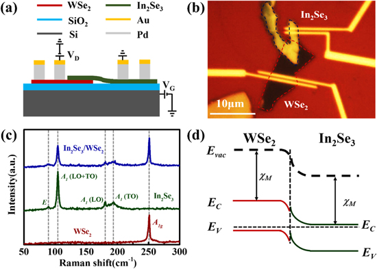
Figure 1. (a) Cross-sectional view of the WSe2/In2Se3 heterojunction device together with the electrical connections used to characterize the heterojunction device. (b) An optical microscope image showing a typical WSe2/In2Se3 heterojunction device next to a WSe2 device and an In2Se3 device fabricated on the same pieces of the 2D materials. Contact electrodes are made of Pd/Au. The WSe2 and In2Se3 nanoflakes are outlined by the red dashed lines and blue dashed lines, respectively. (c) Raman spectra of the WSe2, In2Se3 and the heterojunction regions taken by using a laser with 488 nm wavelength. (d) Energy band diagram of the WSe2/In2Se3 heterojunction in equilibrium, where EC and EV are the conduction band edge and valence band edge, the horizontal straight dashed line marks the Fermi energy level, χM is the electron affinity, and Evac is the vacuum energy level.
Download figure:
Standard image High-resolution imageBefore characterizing the heterostructure device, in order to understand the properties of the components of the heterostructure, we study the FETs based on the same pieces WSe2 and In2Se3 in the heterostructure as shown on figures 1(a) and (b). The source–drain current (ID) is measured at different source–drain voltages (VD) under different gate voltages (VG). As shown in figure 2(a), the WSe2 FET shows roughly linear ID-VD characteristics with different back gate voltages in a large bias range from −1 V to +1 V, indicating that the contact barrier between WSe2 and Pd is very low. The output curves of In2Se3 (shown in figure 2(b)) are linear under small bias voltage and show saturation under large bias voltage, confirming an ohmic contact between In2Se3 and Pd. The asymmetry of ID at VD = ±1 V probably results from the ferroelectric properties of the In2Se3 materials [40]. Moreover, the transfer curves at VD = 1 V in figures 2(c) and (d) show p-type characteristic of the WSe2 device and n-type characteristic of the In2Se3 device, indicating that Pd can efficiently inject holes into the WSe2 channel with a negative gate voltage and efficiently inject electrons into the In2Se3 channel with a positive gate voltage. These results agree with the literature [34, 41]. We note that the drain current is different in the output curve and transfer curve at the same VD and VG. Such current difference could be due to the hysteresis of 2D material devices and the ferroelectric properties of the In2Se3 material [40, 42]. The origins of the hysteresis could be gas adsorption/desorption, intrinsic defects in the 2D materials and in the SiO2 dielectric layer, traps at the interface between the 2D material and SiO2, and water adsorption on the surface of the SiO2, etc. Here, the transfer curves of the WSe2 FET were measured from VG = 10 V to VG = −50 V, while the output curves were measured at VG = −50 V first and at VG = 0 V last with the VG changing step being −10 V. The gate voltage stress could cause different drain currents in the output curve and transfer curve at the same VD and VG [42]. For the In2Se3 FET, besides the hysteresis, the ferroelectric properties of In2Se3 could be for another reason. In2Se3 material has intrinsically intercorrelated out-of-plane and in-plane polarization [43, 44]. High gate voltage and drain voltage can induce ferroelectric polarization in In2Se3 and cause different drain currents in the output curve and transfer curve at the same VD and VG. Here, the transfer curves of the In2Se3 FET were measured from VG = −30 V to VG = 50 V, while the output curves were measured at VG = 50 V first and at VG = 0 V last with the VG changing step being −10 V.
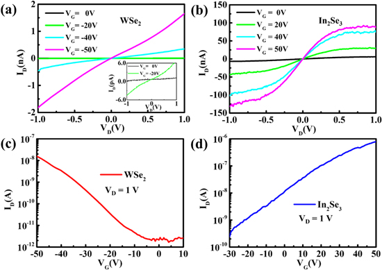
Figure 2. Electrical properties in the dark of the WSe2 device and In2Se3 device shown in figure 1(b). (a) Output curves of the WSe2 FET. (b) Output curves of the In2Se3 FET. (c) Transfer curve of the WSe2 FET. (d) Transfer curve of the In2Se3 FET.
Download figure:
Standard image High-resolution imageAlthough band alignment in heterostructures can be probed by experimental methods, such as scanning tunneling microscopy and spectroscopy, there has not so far been any reported experimental work on the band alignment of a WSe2/In2Se3 heterostructure, to the best of our knowledge. It has been reported that the band gap of WSe2 is ∼1.50 eV at 5 nm and that of In2Se3 is ∼1.45 eV at 20 nm, while the electron affinity (χM) of WSe2 and In2Se3 is 4.0 eV and 3.6 eV, respectively [33, 37, 45, 46]. Based on these data, the energy band alignment of the WSe2/In2Se3 heterostructure without bias voltage is sketched in figure 1(d). A type-II band alignment is formed, where the Fermi level of the WSe2 locates at the edge of its valence band and that of In2Se3 locates at the edge of its conduction band. This kind of heterostructure has a great potential for rectifying devices.
Next, the photoelectrical properties of the WSe2 FET and In2Se3 FET are investigated by exploring their output characteristics at VG = 0 V (when the devices are in the off-state) under the illumination of a laser with various power density, because the photoelectric response is more significant in the off-state than that in the on-state (figure S2). Figures 3(a) and (b) show the ∣ID∣-VD curves of the WSe2 FET and In2Se3 FET in the dark and under the illumination of a laser with wavelength being 650 nm and power density being 2.71 W cm−2. No photovoltaic response can be observed, further confirming the roughly symmetric ohmic contact of the WSe2 FET and In2Se3 FET. The drain current of the WSe2 FET increases by more than two orders of magnitude and that of In2Se3 FET increases more than ten times when the devices are illuminated and ∣VD∣ is larger than 0.3 V. These large current on/off ratios are due to two reasons. First, the current in the off-state is very low, below 10−12 A for the WSe2 FET and below 10−8 A for the InSe2 FET when ∣VD∣ is larger than 0.3 V. Second, the incident light can be effectively absorbed by the multilayered materials and generate electron-hole pairs which can be extracted by the drain–source voltage. The photocurrent IPHOTO is defined as ILIGHT–IDARK, where ILIGHT and IDARK are the ID with and without laser illumination, respectively. Figure 3(c) shows the photocurrent versus light power density at VD = 1 V. For both the WSe2 and In2Se3 FETs, the photocurrent increases with the laser power density due to the increase of photo-induced carriers (figure S3). The relationship between the photocurrent and laser power density can be described by a simple power law dependence of the form IPHOTO = αPβ, where IPHOTO is the photocurrent, α is a constant associated with the light wavelength, P is the laser power density and β is another constant that relates to the device's response to the light [10]. The photocurrent versus light power density of the WSe2 FET and In2Se3 FET exhibit different power law dependence. By fitting the experimental data, β of the WSe2 FET is estimated to be 1.13, while that of the In2Se3 FET is estimated to be 0.47. In the WSe2 FET, the large exponent is probably due to the low and uniform distribution of the trapping center and the low light absorption with the indirect band gap of the multilayer WSe2. As for the In2Se3 FET, the thickness of the channel and the direct band gap of the material can endure the high absorption efficiency of the incident light. The photocurrent follows roughly a square root dependence of the incident laser power density, and this non-integer power dependence could be attributed to a complex process of carrier generation, recombination and trapping along the channel [47, 48].
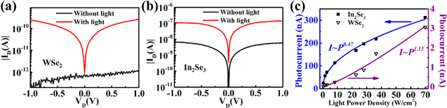
Figure 3. Photoelectrical response of the WSe2 device and In2Se3 device upon the illumination of 650 nm laser at VG = 0 V. The ∣ID∣-VD curves of (a) the WSe2 device and (b) the In2Se3 device with and without light illumination. (c) Photocurrent of the two photodetectors at VD = 1 V as a function of the light power density. The triangles (WSe2) and the squares (In2Se3) are the experimental data. The purple line and the blue line are the fitting results.
Download figure:
Standard image High-resolution imageWe then characterize the heterojunction device in the dark at room temperature. The electrical connections used to perform electrical measurement on the heterojunction device are shown schematically in figure 1(a), where a back-gate voltage applied on the silicon substrate is used to adjust the doping in the channel. Figure 4(a) shows the output curves of the WSe2/In2Se3 heterostructure device at VG = −50 V, 0 V and 50 V. The ∣ID∣-VD curve exhibits strong current rectification property at VG = −50 V with the forward current being much larger than the reverse current. Due to the p–n junction at the WSe2/In2Se3 interface, the reverse current is suppressed to about 10−13 A, which is several orders of magnitude lower than the dark current in the WSe2 FET and In2Se3 FET. The current rectification ratio (or the forward/reverse current ratio) is 7.37 × 10³ at VG = −50 V, which is calculated by dividing the forward current at VD = 1 V by the absolute value of the reverse current at VD = −1 V. This rectification ratio is among the highest in the p–n junction 2D heterostructure devices, as shown in table 1. When VG = 0 V, the output of the heterojunction device shows that the current flowing in the channel is totally suppressed to below 3 × 10⁻¹³ A under positive or negative VD. At VG = 50 V, the ∣ID∣-VD curve shows roughly symmetric behavior with the dark current being still lower than 10−11 A even at ∣VD∣ = 1 V. These output curves of the heterojunction are consistent with type-II band alignment.
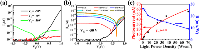
Figure 4. Electrical properties and photoelectrical properties the WSe2/In2Se3 heterojunction photodetector. (a) Output curves of the WSe2/In2Se3 heterojunction device at VG = −50 V, 0 V and 50 V in the dark. (b) ∣ID∣-VD curves of the WSe2/In2Se3 heterojunction device in logarithmic scale in the dark and under illumination of 650 nm laser with various power density. (c) Photocurrent and responsivity (R) of the heterojunction device recorded with various laser power density at VD = −1 V.
Download figure:
Standard image High-resolution imageTable 1. Comparing the characteristic parameters of present devices to those of the WSe2-based and InSe-based 2D materials heterojunction photodetectors in previous reports.
| Materials | VG (V) | VD (V) | λ (nm) | Power (mW cm−2) | R (mA W−1) | Rectification Ratio | ON/OFF Ratio | Τ (ms) | Voc (V) | EQE (%) | References |
|---|---|---|---|---|---|---|---|---|---|---|---|
| WSe2/MoS2 | −50 | −1.2 | 532 | — | 11 | ∼500 | ∼35 | — | 0.55 | 1.5 | [12] |
| WSe2/MoS2 | 0 | −0.5 | 514 | 5 μW | — | — | — | <0.1 | 0.27 | 12 | [29] |
| WSe2/ReS2 | −50 | −3 | 405 | 1.57 | 50 | 700 | — | — | 0.55 | 15.3 | [18] |
| WSe2/ReS2 | −30 | −1 | 640 | 47.8 | 600 | 104 | ∼100 | 2 | 0.3 | 122 | [28] |
| WSe2/SnSe2 | −100 | −3 | 532 | 8nW | 58 800 | — | — | — | — | 1367 | [52] |
| WSe2/BP | −35 | −3 | 532 | 2.6 μW | — | 2500 | — | — | 0.29 | 3.1 | [46] |
| AsP/InSe | 10 | 2 | 520 | 20 000 | 1000 | ∼107 | ∼108 | 0.2 | <0.01 | 1.5 | [19] |
| GaTe/InSe | −30 | 6 | 405 | 6.35 | 13.8 | 1000 | — | 0.02 | 0.4 | 4.2 | [20] |
| BP/InSe | 0 | 0.5 | 455 | 1280 000 | 11.7 | — | 60 | 24 | — | 3.2 | [21] |
| WSe2/α-In2Se3 | −50 | −1 | 650 | 290 (0.51 μW) | 26 | 7.37 × 10³ | 1.24 × 10⁵ | 2.22 | 0.65 | 5 | This work |
As the dark current can be effectively suppressed in the p–n junction device under reverse bias at VG = −50 V when the rectification property is obvious, we analyze the photoelectronic property of the WSe2/In2Se3 heterostructure device at VG = −50 V. The ∣ID∣-VD curves are measured under 650 nm laser with different power densities ranging from 0.29 W cm−2 to 69.81 W cm−2 and the results are shown in figures 4(b) and S4. A photovoltaic response can be seen clearly. In addition, the photovoltage increases with the light power density and reaches the saturate value of 0.65 V (figure S5(a)) when the power density is higher than 8.21 W cm−2. As the channel length of the present devices is longer than 10 micrometers and the laser spot is focused to be small enough to only shine on the channel area, the photovoltaic responses do not come from the contacts. Although photocurrent can be observed in the WSe2 FET and In2Se3 FET, no photovoltaic response can be observed in these devices, as shown in figures 3(a) and (b). Therefore, the response is due to the potential barrier at the heterojunction. The 0.65 V photovoltage is higher than most of the published 2D vdW heterostructure devices based on WSe2 or InSe, as shown in table 1, due to the band alignment of the present WSe2/In2Se3 heterostructure.
The current on/off ratio to the light is more obvious under reverse bias than that under forward bias due to the suppressed low dark current under reverse bias. We notice that the photocurrent of the heterostructure device is higher than the WSe2 FET but lower than the In2Se3 FET under the same negative bias and the same light power density. The current on/off ratio of the heterostructure device is much higher than that of the WSe2 FET and the In2Se3 FET under the same negative bias and the same light power density, due to the p–n junction. The current on/off ratio of the heterostructure device increases with the light power density and reaches 1.24 × 10⁵ when the power density is 69.81 W cm−2 (figure S5(b)). This photocurrent on/off ratio is several orders of magnitude larger than that in most of the previous reports based on WSe2 or InSe, as shown in table 1.
In order to confirm that the above observed photoelectronic properties do come from the heterojunction rather than the influence of the surrounding air, we compare the properties of one device in a vacuum (with the pressure being <1.3 mTorr) and in the air. As shown in figure S6, besides a small shift of the threshold voltage, the electronic property and photoelectronic properties are about the same in the vacuum and in the air. Therefore, the novel properties shown do come from the WSe2/In2Se3 heterostructure itself. Four other 2D WSe2/In2Se3 heterostructure devices have also been successfully investigated and all the devices display similar electronic and photoelectronic properties, suggesting stable photodetecting properties.
The experimental photocurrents as a function of the 650 nm laser power density are fitted with the equation of IPHOTO = αPβ, and β is obtained to be 0.58, as shown in figure 4(c). The non-linear relationship is similar to the result of the In2Se3 FET detector, probably because the photoelectric property of the WSe2/In2Se3 heterostructure device at VG = −50 V is mainly decided by the In2Se3 part and the WSe2/In2Se3 interface. The deviation of β from 1 indicates the loss of photo-induced carriers at the interface of the heterojunction and the increasing recombination process [47, 48].
To further evaluate the performance of the photodetector, several figures of merits are extracted as follows. Responsivity (R) is calculated according to the equation R = IPHOTO/(P × S), where IPHOTO is the photocurrent of the detector, P is the incident laser power density and S is the effective area of the photodetector [10]. Figure 4(c) shows the relationship between the photo responsivity and incident laser power density. The maximum responsivity of the typical photodetector is 26 mA W−1 to 650 nm laser with power density of 0.29 W cm−2 when VG = −50 V and VD = −1 V. It is notable that R decreases with the increasing irradiation power density, which may be explained by a complex process of carrier generation, recombination and trapping existing in the channel or the interface between the channel and the dielectric substrate [47, 49]. External quantum efficiency (EQE) is expressed as EQE = Rhc/eλ, where R is the responsivity of the detector, h is Planck's constant, c is the speed of light in vacuum, e is the electron charge and λ is the incident laser wavelength [10]. EQE decreases with increasing power density, as shown in figure S5(c). The maximum EQE of the typical photodetector we obtained is 5% to a 650 nm laser with power density of 1.52 W cm−2 when VG = −50 V and VD = −1 V. We believe that the responsivity of the heterojunction can be further improved by optimizing the thickness of the materials and improving the crystal quality. Also, if a lower power density could be used, the responsivity and EQE could be higher.
Figure 5(a) shows the photocurrent transient response behavior of the typical heterojunction photodetector shown in figures 1, 3 and 4 to a 650 nm laser with a power density of 2.71 W cm−2. Illumination is switched on and off periodically at 100 Hz using a chopper. The on-off switching behavior can be well retained even after many cycles. With the laser on, the photocurrent increases quickly and then reaches the maximum. When the laser is chopped off, the photocurrent decreases fast and later reaches its initial value in the dark. The photocurrent rise time (which is the time required to raise the photocurrent from 10% to 90% of its maximum value) and fall time (the time needed to reach to 10% of the photocurrent after chopping off the illumination) are crucial parameters in determining a photodetector's response speed to a fast-varying optical signal. Figure 5(b) shows a single on/off cycle of the photocurrent waveform. The rise time is observed to be 2.22 ms and the fall time was 2.38 ms. These response times are shorter than that of In2Se3 FETs and WSe2 FET given in previous reports [34, 36, 50, 51].
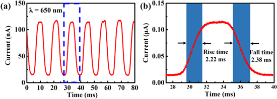
Figure 5. Transient response of the WSe2/In2Se3 heterojunction photodetector under 650 nm laser with VG = −50 V. (a) Temporal photocurrent waveform of the device at VD = −1 V measured using a chopper switched at 100 Hz. (b) A single cycle of the photocurrent waveform showing a rise time of 2.22 ms and a fall time of 2.38 ms.
Download figure:
Standard image High-resolution imageWe then explore the response of the present devices to the light with different wavelengths. Figure 6(a) shows the ∣ID∣-VD curves of the WSe2/In2Se3 heterojunction photodetector measured in the dark and under the illumination of a laser with different wavelengths at VG = −50 V. This photodetector shows a clear response to the light ranging from 650 nm to 900 nm. This phenomenon indicates the device has a multispectral response. The photo responsivity R of the same heterostructure device as a function of the illumination wavelength is plotted in figure 6(b). The device response remains roughly the same from 650 nm to 750 nm and then decreases continuously with the wavelength to a low value at 900 nm. In fact, our device also shows response to the light ranging from 900 nm to 1550 nm (as shown in figure S7), although the responsibility is very low. The primary reason for the decreasing responsivity is the band gap of the materials. Because multilayer In2Se3 and WSe2 have a band gap around 1.45 eV and 1.50 eV, respectively, the light with the wavelength shorter than 750 nm can generate electron–hole pairs through band transition in these semiconductors [33, 37, 45, 46]. For the wavelengths longer than 750 nm, oxygen absorption and oxygen-associated selenium defects could induce the photo response of In2Se3 to light with a long wavelength beyond the band gap [36]. The enhancement of the built-in electronic field at the heterojunction induced by the extremely negative gate voltage and the high reverse voltage may also contribute to the response to the light with long wavelength [52]. The edges of the conduction and the valence band are tilted along the direction of the electronic field. The wave functions of the electron and hole can extend a tail into the forbidden band increasing the e–h interactions with the sub-band gap photons [52–54]. Thus, a photon with the energy smaller than the band gap of WSe2 and In2Se3 can allow the photo-excited carrier generation.

Figure 6. Wavelength-dependent properties of the WSe2/In2Se3 heterojunction photodetector with VG = −50 V. (a) ∣ID∣-VD curves of the WSe2/In2Se3 heterojunction photodetector in logarithmic scale in the dark and under illumination of the light with different wavelengths. (b) Responsivity of the photodetector to the light with different wavelengths extracted at VD = −1 V.
Download figure:
Standard image High-resolution image
Finally, we compare the relevant figures of merit of the present devices with that of the state-of-the-art vdW p–n heterojunction 2D material photodetectors based on WSe2 or InSe in table 1. It can be seen that the performance of the present WSe2/In2Se3 heterojunction photodetector is comparable with that of the best vdW p–n heterojunction photodetectors. The attractive performance of the present devices is attributed to the following. First, the direct band gap of the material endures high absorption efficiency of the incident light. Second, the heterojunction devices possess the built-in electric field, so the photo-induced carriers can be quickly separated. Third, the p–n junction suppresses the dark current very effectively. The good ohmic contacts also benefit the collection of the photo-induced carriers.
Conclusions
In summary, for the first time, we demonstrate vdW heterojunction photodetectors based on p-type few layer WSe2 and n-type multilayer α-In2Se3 with direct band gap. Pd electrodes appear to form good ohmic contacts with both the materials. The p–n junction heterojunction has an extremely low dark current of 10−13 A under −1 V bias and a current rectification ratio as high as 7.37 × 10³ in a bias voltage range of ±1 V at VG = −50 V. To the laser with wavelength of 650 nm, the heterojunction devices exhibit a photocurrent on/off ratio of 1.24 × 10⁵ and a maximum photo responsivity of 26 mA W−1. The photodetector also has fast and reproducible photocurrent switching behavior with the photoresponse rise time being 2.22 ms and the fall time being 2.38 ms. The photodetectors also show response in a range from 650 nm to 900 nm. Our work demonstrates an attractive platform utilizing heterojunction based on multilayer In2Se3 with a direct band gap for high performance optoelectronic devices.
Methods
Devices fabrication
Multilayer WSe2 was exfoliated from a bulk material brought from HQ graphene and then put onto a p++ Si wafer covered by a 300 nm SiO2 layer. Multilayer In2Se3 was exfoliated from a bulk material bought from HQ graphene and then put onto another Si/SiO2 substrate. The multilayer In2Se3 on the Si/SiO2 substrate was picked up and then released on the few layer WSe2 by using a poly propylene carbonate coated polydimethylsiloxane block mounted on a glass slide [55, 56]. Electrical electrodes were designed by electron beam lithography (Raith 150-Two) and then 80 nm-thick Pd and 30 nm-thick gold were deposited by electron beam evaporation. Pd was used to contact both the In2Se3 and WSe2 not only due to the technical simplicity, but also because Pd has been confirmed to form ohmic contact with In2Se3 [36] and can effectively inject holes into the WSe2 channel.
Optical measurement
The Raman spectra were measured using a laser with 488 nm wavelength and the power of 2.89 mW on a HORIBA LabRAM HR800 micro-Raman system. The measurements were performed using a grating of 1800 gr mm−1 for high resolution. The objective lens with a magnification of 50 was utilized. Each spectrum was acquired in 10 s.
AFM measurement
A Dimension 3100 AFM working at tapping mode was used to measure the thickness of the materials. The measurements were carried out at room temperature in the air.
Electronic and photoelectric measurement
The electrical and optoelectronic characteristics of all the devices were measured using a Keithley 4200-SCS system and a probe station. The optoelectronic measurements were performed in the air at room temperature on a HORIBA LabRAM HR800 system with NKT EXR-15 supercontinuum laser sources. The photocurrent transient response behavior was measured with an oscilloscope (Agilent DSO7054A).
Acknowledgments
This work was supported by the National Natural Science Foundation of China (Grant No. 61775006, 61621061 and 21573014). J Liao was also supported by the National Key R&D Program of China (Grant No. 2017YFA0204903 and 2016YFA0201901).