

Abstract
Resistive switching in nanostructured metal oxide semiconductors has been broadly understood to originate from the dynamics of its native point defects. Experimental results of switching observed in individual n-ZnO nanorods grown on a p-type polymer is presented along with an empirical model describing the underlying defect dynamics necessary to observe bi-polar switching. Selective photo excitation of electrons into the defect states delineates the incidence and role of an ionic current in the switching behavior. The understanding further extends to the observance of a negative differential resistance regime that is often coincident in such systems. The analysis not only unifies the underlying physics of the two phenomena but also offers further confidence in the proposed mechanism. We conclude by demonstrating that the effective memresistance of such devices is a strong function of the operating bias and identify parameters that optimize switching performance.
Export citation and abstract BibTeX RIS
1. Introduction
The memory resistor or memristor, that has been described as one of the fundamental passive circuit elements of electronics, along with resistors, capacitors and inductors, is however not ubiquitous like the others [1, 2]. In spite of the fact that electrical properties of a memristor is an integral requirement of most modern electronic memory and storage devices. Over the past decades, a variety of electrical and magnetic [3–7] systems have been investigated for the purpose, amongst which resistive switching memory (RSM) devices have emerged as promising candidates for the future [8, 9]. RSMs generally consist of a resistive 'active' layer sandwiched between two conducting electrodes (not necessarily metals) that typically form a double diode configuration displaying hysteretic IV characteristics with distinct resistances in a high resistance state (HRS) and a low resistance state (LRS). RSM has been observed in a range of complex oxides [9–14], in systems that sustain an ionic current in addition to the electronic component. Metal oxide based RSMs have gained further interest due to its wide range of electrical properties, fast operating speed and low power consumption [15–18]. ZnO is one such 'active' component that has been investigated previously due to several advantages pertaining to its ease of fabrication, inherent multi-functionality, control of switching properties through doping and alloying [14, 18–27] and availability in a wide range of low-dimensional nanostructured forms.
Investigations on ZnO based RSMs have explored a range of device architectures including stacked metal electrodes [18, 19, 28], multilayer structures [29–32], doping [23–26] and engineered nanostructured morphology [33, 34]; a majority of which have used its nanostructured form to evidence the phenomena. The present study reports bipolar RSM in individual ZnO nanorods (ZNRs) in a double diode configuration, configured as Pt/n-ZnO/p-poly(3, 4-ethylenedioxythiophene)-poly(styrenesulfonate) (PEDOT:PSS). Supplementing the extensive optoelectronic capabilities of n-ZnO/p-PEDOT:PSS hybrid devices, e.g. light emitting diodes and photo-detectors [35, 36], with RSM capability paves the way towards further multi-functional integration of ZnO based devices. Interestingly, RSM in ZnO nanostructures have occasionally shown to be accompanied by the incidence of negative differential resistance (NDR) regions in their current–voltage (IV) characteristics [12, 30–34], as is the case in the present study. In line with the accepted view, we argue that RSM in ZnO originates from the presence of mixed electronic-ionic transport processes i.e. in addition to the generic electronic transport, an ionic channel (ionized oxygen vacancies,  ) in ZnO is essential for observance of the phenomena. Existence of the ionic channel has been explored in the conducting filament (CF) model, that envisages voltage induced formation (and rupture) of extended CFs of the ionized vacancies [9–11, 18, 26, 37]. Some have argued for voltage stimulated physical diffusion of oxygen (or other defect) vacancies through the active media, especially across surfaces as pathways of the ionic current [10], while others have explained the observations in terms of a surface chemisorption process [38]. The processes involved still remains ill understood in terms of the physical kinetics and even identity of the participating ionic species. The native n-type conductivity in ZnO, and other metal oxides, is understood to originate from ionization of native point defects (NPDs) i.e. donor type dopants
  and interstitial zinc (IZn) [39], which are also assumed to play a significant role in the observed switching behavior via the ionic current. The probability of ionization of any sub band gap defect states is dependent on the local position of the Fermi level (EF) vis-à-vis the valence band (VB), conduction band (CB) and the defect states. Thus the relative abundance of ionized dopants is strongly coupled to parameters that affect EF, e.g. local electron density and applied bias. The coupling to external bias is readily evidenced, for example via existence of the critical 'set' and 'reset' voltages in RSM devices [40] and has been well documented. However, the effect of changing the local electron density, that may be readily altered, selectively excitation to the CB or to the defect states using suitable optical illumination [32, 38, 41] has largely remained unexplored. We investigate switching under optical excitation at two wavelengths, (i) λ1 = 355 nm, hv = 3.49 eV which is higher than ZnO's optical band gap (Eg = 3.3 eV) and (ii) λ2 = 532 nm, hv = 2.33 eV that approximately corresponds to the energy difference between the VB edge and the sub-band gap oxygen defect states in ZnO. While λ1 creates electron–hole pairs between the conduction and VB, λ2 excites electrons from VB to the oxygen vacancy states [39, 42, 43]. Though both photo-generate carriers in ZnO and increases conductivity, only the λ2 excitation directly addresses the
  states. Changes to the switching behavior, evidenced by the cyclic IV characteristics, obtained with and without illumination offer insights to comprehend the switching process and directly evidences existence of the ionic conduction channels which is then modeled mathematically. The model developed, also offers an understanding of the generic configurational requirement of either a Schottky or pn junction or both at either ends of the active layer to experimentally realize switching behavior. Finally, we quantify the memresistance (M) parameter of the device, its bias dependence and evolution with optical excitation in order to optimize the switching parameters, i.e. on–off ratio, endurance and retention. The study also explores the feasibility of growth of ZNRs directly onto a conducting polymer, the use of which as the substrate takes another step towards flexible device fabrication.
2. Experimental details
To realize the memristor device shown in figure 1(a), ZNRs were electrochemically grown directly on a PEDOT:PSS layer to fabricate a pn heterojunction. A Zn foil (Sigma Aldrich) was prepared by sequential sonication in acetone, ethanol and deionized water, followed by ozone cleaning prior to spin coating of ∼20 μm thick film of PEDOT:PSS (Sigma Aldrich), with sequential rotation speeds of 1000 rpm and 3000 rpm for 10 s and 30 s, respectively. The coated substrate was then baked at 200 °C in N2 atmosphere and subsequently used as the working electrode in a two-step ZNR electrochemical growth process. The ZNRs were grown in an electrochemical bath of 25 mM equimolar aqueous solution of zinc nitrate hexahydrate (Sigma Aldrich) and hexamethylene-tetramine (Sigma Aldrich) at 95 °C, using a platinum wire as the counter and reference electrodes. The PEDOT:PSS coated substrate was then sequentially biased at −2.73 and −2.15 V, relative to the reference electrode, for 1 and 20 min respectively. Further details of the ZNR growth process have been published elsewhere [39]. The ZNR covered substrate was rinsed in deionized water and dried at 65 °C for 30 min, prior to morphological characterization which was performed using Nova Nano SEM 450 field-emission scanning electron microscope (SEM) coupled with an Apollo X energy dispersive x-ray analysis (EDS) system and 300 kV FEI TECHNAI G2-TF-30 transmission electron microscope (TEM). The conducting atomic force microscope (CAFM) tip of a MultiMode 8™ AFM (Bruker Inc.) contacting the top surface of individual ZNRs was used to perform the electrical characterization performed here. A platinum coated cantilever tip (MikroMasch, HQ:XSC11/Pt, k = 0.4 N m−1) in 'contact' with the top surface of the ZNRs, in conjunction with the conducting substrate formed the end electrodes across the active ZnO device (figure 1(a)). After mapping the surface topography of the device, the cantilever was fixed on top of individual hexagonal ZNRs to obtain the device current–voltage (IV) characteristics. The IV characteristics were obtained, at a constant tip loading force of 17 nN, by ramping the dc bias (Vb), applied to the Zn substrate, between ±5 V and the virtually grounded CAFM tip connected to a current amplifier of gain 107 V A−1. In addition to the IVs recorded in the dark, IVs were also recorded with the tip-sample junction illuminated with continuous wave laser excitation at wavelengths λ1 (355 nm ± 3 nm) and λ2 (532 nm ± 3 nm) to study the photoresponse (PR) of the devices. Further details of the above AFM based measurement setup are available elsewhere [42]. To confirm the robustness of the data presented here we have recorded over 50 sets of IV characteristics on different ZNRs in dark and optical excitations, each. From which 30 sets of IVs, corresponding to stable junctions i.e. IVs devoid of drift and noise, have been used for performing further mathematical analysis. All samples were stored in the dark for extended periods between experiments and all AFM experiments were conducted in the ambient.
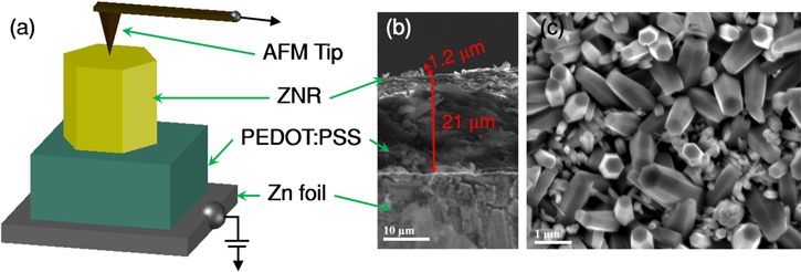
Figure 1. (a) Schematic of the RSM device composed of ZnO nanorods grown on PEDOT:PSS covered Zn foil (b) cross-sectional SEM images of nanorods grown on PEDOT:PSS layer (c) electrochemically grown hexagonal ZnO nanorods on PEDOT:PSS show a diameter variation from 200–700 nm with the height of ∼1 μm.
Download figure:
Standard image High-resolution image3. Results and discussion
Figure 1(b) shows the cross-sectional SEM image of ZNRs electrodeposited on PEDOT:PSS coated Zn foil. The image shows c-axis oriented ZNRs of heights ∼1 μm grown above a ∼20 μm thick PEDOT:PSS layer. Figure S1(a) in the supplementary material is available online at stacks.iop.org/NANO/29/105701/mmedia and shows the high resolution TEM image of a ZNR confirming the crystallinity of the sample and [0001] axis growth. The EDS spectrum in figure S1(b) confirms that, the as-synthesized ZNRs are composed only of zinc and oxygen elements. Figure 1(c), showing a top view SEM image of the ZNRs evidences a spread in nanorods diameter varying between 200 and 700 nm, which arises primarily due to the absence of any pre-growth seeding step is known to effect a higher uniformity in nanorod diameter. The cross-sectional image (figure 1(b)) shows the ZNRs to be well isolated from the underlying Zn substrate via the PEDOT:PSS layer, ensuring electrical transport through the ZNRs pass via the pn heterojunction to the underlying Zn. Figure 2(a), showing a dark IV characteristics recorded for a point contact of the CAFM tip on a single ZNR, is representative of the typical bipolar switching cycle observed in the devices investigated. The current amplifier gain restricts the output current upto ±1 μA maximum, limiting the detected current values. The hysteresis evidences existence of a HRS and a LRS of the device that were recorded when Vb was swept from −5 V to +5 V and reverse, respectively. In order to confirm the stability and reproducibility of the switching process, dc voltage sweeps between ±5 V were performed ∼50 times for each point contact in the dark. Figure 2(b) plots the device dc resistance, at Vb = −0.5 V in each switching cycle, demonstrating endurance performance over 50 cycles with a stable dc resistance off/on (HRS:LRS) ratio ∼103. The reproducibility of the switching behavior and the high off/on ratio illustrates the functional robustness of the device as a memristor. In the HRS, the IV curve (black dots in figure 2(a)) is characterized by a turn-on voltage (VON ∼ 0.7 V) under positive bias, which is absent in the LRS. The LRS state is characterized by a well-developed NDR region between biases V1 (≃ –0.5 V) and V2 (≃ –1.5 V), within which the current decreases in magnitude with increasing ∣Vb∣. The limits, V1 and V2 demarcate the onset and termination of the NDR region characterized by a local 'minima' and 'maxima' in the IV plot.

Figure 2. (a) CAFM point IV spectra, recorded in dark, exhibiting bipolar switching. The arrows indicate direction of the voltage sweeps. The LRS characteristics (Vb ramped from +5 to −5 V) region has been fitted to equation (4), as discussed in the text and (b) device endurance performance at Vb = −0.5 V, for 50 cycles of the RSM device.
Download figure:
Standard image High-resolution imageFigure 3(a) shows the IV characteristics of a point contact, in dark and under illumination at the two wavelengths, λ1 and λ2. Though current and conductivity increase were detected across all Vb for both excitations, the increase under negative polarity was markedly different than that under positive polarity. Figure 3(b) shows the numerically calculated dI/dV versus Vb plots obtained in the LRS state corresponding to Vb sweep from +5 to –5 V. In the dI/dV plots the NDR region is demarcated by negative values of differential conductance. Below we summarize the salient features of the IV and dI/dV data that needs to be noted prior to further analysis. Firstly, the NDR regime appears selectively for Vb < 0 and only in the LRS. Further, the device conductance in the LRS, for Vb > V1 under λ1 and λ2 illumination are comparable in magnitude with similar bias dependence, which are however distinctly different from that observed in the dark. This similarity in behavior under λ1 and λ2 excitations is evidenced in spite of their very different photogeneration pathways in ZnO. That is while λ1 excites electrons from valence to conduction band, λ2 excites electrons from the valence to the intermediate  defect states [39]. But within the NDR region the magnitude of dI/dV values are higher under λ2 compared to those for dark and λ1, which yield dI/dV of comparable values. Finally, the width of the NDR region (∣V2 – V1∣) is widest in the dark followed by that under λ2 and narrowest under λ1 i.e. the termination voltage of the NDR region, V2 is strongly influenced by illumination wavelength, unlike V1, which remains relatively unchanged under photo excitation, V2 changes from –2.0 V to –1.75 V and –1.3 V for dark, λ2 and λ1 illumination, respectively. It is relevant to note here that PEDOT:PSS shows no absorption [44] or PR [43] in the spectral range (300–1200 nm) thus the observed PR is understood to arise entirely from that of ZnO and changes to the junction properties due to photogeneration of carriers in ZnO.
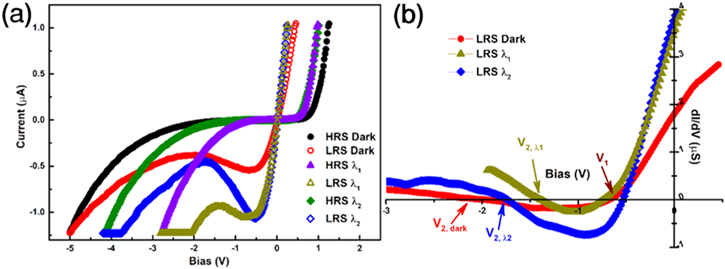
Figure 3. (a) Point IV spectra on a single ZNR in dark and with λ1 (355 nm) and λ2 (532 nm) illumination. The flat current regions for –ve bias occurs due to saturation of the current amplifier output. (b) Numerically differentiated dI/dV spectra from the LRS of IV data.
Download figure:
Standard image High-resolution imageTo comprehend the observed electrical characteristics, switching and NDR, we model the device response in terms of an equivalent electrical components and their idealized IV characteristics. We consider the Pt/n-ZnO/p-PEDOT:PSS hybrid device to have a double diode configuration, composed of back-to-back Schottky (Pt/n-ZnO) and pn (n-ZnO/p-PEDOT:PSS) junctions. The understanding being that the overall transport is described by transport across the junctions coupled with conduction through the ZNRs. The energy band diagram of such a device, at equilibrium (Vb = 0), is shown in figure 4(a). Figures 4(b) and (c) depicts the changes in the energy profile under negative and positive Vb applied to the PEDOT:PSS terminal with respect to the Pt tip held at virtual ground potential. Figure 4(d) indicates the unmodified energy levels of Pt, ZnO and PEDOT:PSS individually, prior to device formation. Here, PEDOT:PSS is modeled as a highly doped p-type semiconductor, as dictated by its HOMO-LUMO energy levels, forming the PEDOT:PSS/ZnO pn junction. Such designation is commensurate with previous reports on photovoltaic properties of ZnO/PEDOT:PSS junctions [43]. Its worth noting that ZnO/PEDOT:PSS junctions have also been modeled as Schottky junctions with effective barrier heights ∼0.7–0.9 eV [45–47], primarily due to the high rectification ratio observed in those investigations. However, the IVs presented here show finite conductance even under negative bias thus justifying the above designation of a pn junction. As shown in figure 4(a), the EF aligns across the entire device, at equilibrium (Vb = 0), effected by substantial band bending in ZnO at both junctions. Consequently this positions the deep level oxygen vacancy states (VO), energetically closer to (or even above) the Fermi level, thereby increasing their probability of ionization into  states [43, 48]. The depletion regions therefore harbor a larger fraction of ionized VO states than the bulk of a ZNR, creating a spatial inhomogeneity in free local electron density along the ZNRs. Figure 4(b) shows the modified band diagram for a large negative bias applied to PEDOT:PSS, whence current flows from Pt to PEDOT:PSS, with the Schottky junction forward biased and the pn junction reverse biased. This decreases the depletion width in ZnO at the Pt interface and increases the width at the PEDOT:PSS interface, thereby increasing the band bending and with it the relative abundance of ionized oxygen vacancy states
  at the PEDOT:PSS interface. Accumulation of
  states at the ZnO/PEDOT:PSS interface is illustrated schematically in figure 4(e). As the negative bias magnitude is decreased to zero, a to b region of the IV curve in figure 2(a) is generated. The bias dependence in the HRS for Vb < 0 is described by that of a forward biased Pt/ZnO Schottky junction along with a large resistance in series; the high resistance simulating the effect of transport across the ZNR and the reverse biased pn junction at the other end (see supplementary material for further details).

Figure 4. Energy band diagram of the Pt/ZnO/PEDOT:PSS device with the Pt tip grounded and (a) zero (b) negative (pn in RB and Schottky in FB) and (c) positive (pn in FB and Schottky in RB) bias applied to PEDOT:PSS. (d) Depicts energy band diagram of Pt/ZnO/PEDOT:PSS separated system. (e) and (f) Show schematic representation of ionized  states accumulating in ZnO at PEDOT:PSS and Pt junction under negative and positive bias, respectively.
Download figure:
Standard image High-resolution imageAs the bias polarity changes to positive, the device current increases abruptly beyond the turn-on bias, VON. The progressively increasing band bending (figure 4(c)) at the now reverse biased Pt/ZnO Schottky junction then accumulates a  interfacial layer in ZnO, as shown in figure 4(f), accompanied by an enhanced electron density in the CB. The nature of band bending in ZnO (figure 4(c)) at the Schottky junction mimics the case of field emission [49], where the strong internal electric field in ZnO, locally narrows the barrier width assisting electron tunneling from Pt to ZnO thereby increasing the conductance of the Schottky junction, even under reverse bias. This coupled with the forward biased pn junction at the ZnO/PEDOT:PSS interface contribute to a rapid increase in the device current for Vb > VON, as seen in figure 2(a) (region c to d). With increasing positive bias the Schottky junction behaves increasingly like an ohmic contact with a forward biased pn junction at the other end. Indeed, the standard methodology of creating an ohmic contact on a semiconductor is by increasing the local electron density by doping, as happens here by ionization of the oxygen vacancy states in ZnO at the Schottky junction. The tunneling conduction across the Schottky junction is crucial since Schottky barriers do not support minority current unlike that across a pn junction. The asymmetric IV characteristics seen in section (a – b – c – d) of figure 2(a), that is the HRS of the device is adequately explained by the conduction mechanism discussed above. As the positive Vb is lowered from its positive maximum (i.e. from +5 V) the slow ionization dynamics of the NPDs
  freeze the overall conductance of the device i.e. even though the positive bias is reduced the ionized NPDs accumulated at the Schottky junction do not deionize readily. The conductance of device, dominated by electron tunneling at the Schottky interface thus locks on to a high conducting or LRS, as evidenced by a almost linear IV characteristics in the region marked (e – b) in figure 2(a). Note that the IV characteristics in (e – b) region is conspicuous by the absence of finite VON in the reducing voltage sweep, which may be understood in terms of the slow ionization dynamics of the
  defects. Based on the above discussion, below we model the IV characteristics in the LRS state i.e. as the device bias is changed from +5 to −5 V.
The 'linear' IV characteristics observed in the region demarcated by (e – b) in figure 2(a) may be phenomenologically modeled as;

where It is the device current and α is a positive constant denoting the slope of the IV data in this regime. Its worth noting that the first experimentally demonstrated case of NDR was observed in the context of the Esaki tunnel diode where the low bias current is likewise borne by tunneling electrons across a highly degenerately doped pn junction [49] and demonstrates a linear bias dependence, for Vb ∼ 0 V, as seen here. As Vb crosses over to small negative values the NPD ionization probability increases towards the pn junction, from the Pt/ZnO interface initiating an effective ionic current originating from the ionization dynamics of the NPDs along the length of the ZNR. In this regime the overall device current then is decided by two inter-dependent current sources or components, (i) transport across the Schottky junction and (ii) the diffusion or redistribution current of the ionized NPDs. The ionic current is expected to become negligible for large negative bias and thus may be modeled as a decaying current Id, for Vb < 0 V, as;

where A and β are constants. It is physically reasonable to assume that the two current sources are inter-dependent and limits each other (i.e. connected in series) because the CB electron density in ZnO, which determines its electrical conductance and transport, originates from the incidence and distribution of ionized NPDs in the ZNRs. Thus the above current components It and Id have interdependent origins and appear effectively as two current sources connected in series. At low to medium negative Vb across the device, Id, is large since the bias reversal initiates significant changes to band bending but overall transport is limited by charge transport across the Schottky junction. The ionized NPDs redistribution dynamics time scale is understood to be much larger than that of electron transport [13] such that It dominates the transport till Vb ∼ −0.5 V. At higher negative bias the increasingly large It gets limited by Id, reflected in the overall decrease in device current. The combined effect of a linearly increasing It and exponentially decreasing Id, with bias gives rise to the minima at bias V1, above which the total current decreases with the increasing magnitude of negative bias giving rise to the NDR region between V1 to V2 bias (f – g in figure 2(a)). The increasing negative bias causes the  defects to deplete from the Schottky interface and re-accumulate at the PEDOT:PSS junction, causing the Pt/n-ZnO junction to resume its Schottky like behavior. At large negative bias thermionic emission (TE) across the Schottky junction dominates the device IV characteristics (g to a in figure 2(a)), such that the current is given by a typical thermionic-diffusion current expression given by;

where, B and γ are constants. For Vb ≤ V2, the TE current dominates carrier transport in the device, which also decides the terminal voltage of the NDR region, V2. Thus the total current I for the voltage sweep of +5 to −5 V i.e. in the entire LRS, including the NDR region, may be expressed as,

Figure S2 in supplementary materials shows the fit to the above equation over the entire LRS regime for the dark IV characteristics shown in figure 2(a), along with the different calculated current components. The best-fit parameters are tabulated in the first row of table 1.
Table 1. Average values of fit parameters in equation (4) obtained by fits to 30 IVs each in the dark and under λ1 (355 nm) and λ2 (532 nm) illumination. The spread in the values obtained from IVs analyzed are denoted alongside. The number in the bracket denotes the typical fit error in individual parameter, in each IV.
| Parameters | α | A | β | B | γ |
|---|---|---|---|---|---|
| Dark | 2000 ± 200 (<0.5%) | 2000 ± 350 (<1%) | 1.4 ± 0.1 (<1%) | 300 ± 50 (<2%) | 0.34 ± 0.04 (<1%) |
| λ1 (355 nm) | 3700 ± 700 | 2200 ± 200 | 1.5 ± 0.2 | 600 ± 80 | 0.38 ± 0.08 |
| λ2 (532 nm) | 4000 ± 500 | 3000 ± 300 | 1.9 ± 0.2 | 300 ± 30 | 0.44 ± 0.01 |
The observed change in IV spectra (figure 3(a)) upon characteristic illumination (λ1 and λ2) then provides an independent control over carrier density in ZnO that is changed at a constant Vb. When the device is illuminated with λ1 or λ2 excitation, e–h pairs are selectively created in ZnO resulting in higher carrier density that effectively increases the conductivity of ZnO. The IV characteristics in the LRS state though substantially modified under illumination is still well modeled in terms of equation (4), the fits to which are shown in supplementary figure S3 and the parameters tabulated in table 1. Close to zero bias where the IV is linear, the parameter α that quantifies device conductance, doubles in magnitude under both illumination (see figure 3(b)). As mentioned earlier, λ1 and λ2 illumination have very different effects in ZnO. Specifically λ2 excitation, which addresses defect states related to the oxygen vacancies [42, 43], has a significant effect on the corresponding ionic current component Id. Table 1 shows that the parameters A and β, which quantify Id, changes significantly compared to the values for dark IVs, but only for λ2 illumination and remains largely unaffected under the super-bandgap, λ1 illumination. Excitation of electrons to ionized VO states, as expected under λ2 illumination would adversely affect ionization of the oxygen defects and consequently decrease the current Id, much sharply with bias as indicated by the distinctly larger values of A and β. Thus the slow but dynamic, ionized defect distribution that was controlled by only Vb and the resulting EF across the ZNR in the dark is substantially weakened and more effectively quenched for Vb < 0, under λ2 illumination. By contrast, the ITE model parameters B and γ show higher sensitivity to λ1 illumination than λ2. This large increase in ITE, with λ1 excitation stems from photoexcitation of electrons (majority carriers) to the CB of ZnO, unlike that for λ2. Thus the difference in the photo-response under the two illuminations clearly distinguishes the different current components discussed above. The stronger ITE under λ1 and the faster decaying Id under λ2 together leads to a smaller magnitude of V2 for λ1 compared to λ2. The NDR regime is then understood to be resulting from interplay of the current components discussed above. Further the analysis shows that the coincidence of NDR with bipolar switching as reported earlier [12, 31–33], is not incidental but originates from the intrinsic dynamics of the ionic current in the metal-oxide layer that is responsible for both phenomena. To the best of our understanding cases of absence of NDR regimes in devices that nevertheless show switching [18, 23, 26, 37] then may be attributed to a relatively weak ionic current component, attributable to the size or surface to volume ratio of the nanostructures in the active layer [34] or perhaps more importantly the nature of the junctions [12] at either end, the importance of which cannot be over stated. Indeed Yang et al [31] observed disappearance of the NDR regime with increased loading force between an AFM tip and the underlying ZnO nanostructure, which they attributed to an interfacial air gap below the ZnO nanostructure. Therefore it is imperative that future research into RSM devices prioritize characterization of the 'contacts' along with that of the active layer, for evidently ideal ohmic contacts across active layers do not lead to either resistive switching devices or NDR regions. As mentioned earlier, previous reports on resistive switching in ZnO nanostructures have explained the phenomena based on the kinetics of ionized NPDs and the ensuing ionic current, where the ionized oxygen vacancies are either physically driven across the active layer or form filaments of the same dynamically. The model presented above envisages a different scenario, where dynamical change to EF across the width of the active layer and junctions at either end changes the local density of ionized donor species and by consequence the local carrier density without a generic requirement of physical defect diffusion or mobility. Optical excitations, directly addressing the same defect states then alter the strength of the ionic current channel. It is also worth noting that adsorption of atmospheric oxygen onto the surface of ZNR plays an important role in deciding their overall conductance [42, 50, 51] and likely the switching behavior. Future investigations into RSM with varying oxygen partial pressure would help elucidate their operational relevance in such devices.
The analysis would be incomplete without discussing the effect of illumination on the actual memresistance (M) of the devices. In published literature, M is identified as the parameter that quantifies electrical resistance memory in the LRS and HRS and has been defined by the equation  [1, 52] where
  is the time integral of the electromotive force or voltage across the device and q is the charge calculated by time integral of the device current. The parameters
  may be computed by integrating I(t) and V(t) components of the recorded IV characteristics, noting the time variation of applied bias i.e. the bias ramp rate, for the cycles −5 to +5 V (HRS) and then +5 to −5 V (LRS). M is then readily calculated from the resulting
  curve by numerical differentiation. To comprehend the physical meaning of M, IV characteristics of gedanken ideal bipolar memristor is shown in figure 5(a). The device shows high and LRS giving rise to two distinct linear IV curves, black and orange respectively. Figure 5(b) shows the corresponding M as a function of bias in the two states, calculated following the method outlined above. In this case the M changes from 5 to 40 MΩ from LRS and HRS, which are expectedly independent of the applied bias. Figure 5(c) then shows a set of extrapolated IV characteristics of a real device, obtained using equation (4) for the best fit parameters for the 'dark' IVs in the LRS state. Figure 5(d) shows the corresponding M versus Vb plot calculated from data in figure 5(c). Unlike the ideal case M is now highly bias dependent. It may be easily shown that for devices with dominantly resistive impedance, M may be more readily estimated from the dc resistance measured at a given bias [13]. Figure 6 shows the MV curves corresponding to the actual device IVs recorded in the dark along with those obtained with λ1 and λ2 excitations, shown in figure 3(a). The M off/on ratio (Moff/Mon) obtained at Vb = −0.5 V (shown by the vertical line in figure 6) ∼103 matches the endurance performance data presented in figure 2(b), where the device resistance was directly measured in the on (LRS) and off (HRS) states at Vb = −0.5 V. The relevance of the MV plot lies in its ability not only to quantify the parameter M but in identification of an optimal voltage range for reading the 'state' of the device i.e. the bias at which the device shows the highest off/on ratio, which lies just above −0.5 V for the data presented here. Under illumination the peak of the MV curves systematically shifts towards zero bias indicating that for systems with higher electron density the optimal operating regime will occur at lower bias. It also indicates that under super-band gap illumination the off/on ratio decreases from that in the dark due to strengthening of the electron current in comparison to the ionic current. This behavior is however contrary to another report on photo stimulated switching [38] observed on gold coated ZnO nanowires, which observed switching only under UV illumination and none in the dark. Optical excitation, especially at λ1 would result in large increase in carrier density affecting both the LRS and HRS, which is shown here to be detrimental to the performance of the switching device. Thus while finite conductivity of the active layer is essential for a memristor operation, high conductivity of the active layer is undesirable necessitating optimization of the doping level to control device performance. The nature of the plots presented in figure 6 also indicates that the set and reset voltages might be lowered in these devices upon optical excitation [38] which is also to be expected from the band bending model discussed earlier in the presence of increased electron and hole density in ZnO, which would substantially reduce the depletion width in ZnO and with it the fraction of ionized oxygen vacancy states at the junctions. Thereby requiring smaller bias to effect switching between the states.

Figure 5. (a) Linear IV characteristics of an ideal switching resistor exhibiting the high and low resistance states. (b) Corresponding memresistance of the states depicted in (a). (c) Idealized device IVs following experimental data shown in figure 2(a). (d) Corresponding memresistance of (c), indicating strong bias dependence that was absent in the idealized linear case.
Download figure:
Standard image High-resolution image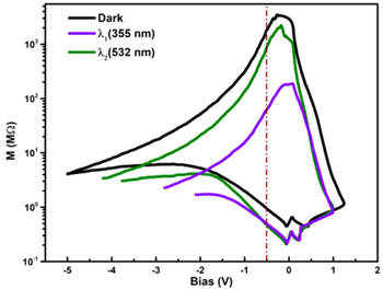
Figure 6. Calculated memresistance versus bias for the device in dark and under illumination. Vertical line indicates –0.5 V bias.
Download figure:
Standard image High-resolution image
4. Conclusion
To conclude, we investigated bipolar resistive switching observed in Pt/n-ZnO/p-PEDOT:PSS devices through current–voltage measurements that also evidenced robust NDR regions. The device memresistance changed by three orders in magnitude as the device moved from the high to low resistance and vice-versa, reproducibly over multiple cycles. The current–voltage characteristics recorded in the dark along with those recorded under ZnO's super- and sub-band gap optical excitation allowed development of a mathematical model to describe the switching phenomena. The model explores the scenario in which the varying position of the Fermi level along the ZNRs and at the active layer and junctions, dynamically changes the local density of ionized donors, consequently generating an effective ionic current through the device, in contrast to erstwhile models based on the diffusion of NPDs as a function of bias. Significantly, transport characteristics obtained with sub-band gap illumination, addressing the oxygen vacancy states of ZnO delineates existence of the ionic current channel providing further confirmation of their involvement in the switching behavior. Finally, the device memresistance is shown to be significantly affected by optical excitation modifying not only the switching on/off ratio but also the set and reset bias voltages.
Acknowledgments
Authors acknowledge financial support from UKIERI-UGC, Government of India, and SERB, DST, Government of India and Royal Academy of Engineering, UK. KB and KNP acknowledge PhD studentship from IISER Thiruvananthapuram.