


Abstract
Several of the scanning probe microscopy (SPM) techniques, such as the scanning tunnelling microscopy (STM) or conductive atomic force microscopy (C-AFM), rely on precise measurements of current flowing between the investigated sample and the conductive nanoprobe. The parameters of current-to-voltage converter (CVC), which should detect current in the picompere range, are of utmost importance to those systems as they determine the microscopes' measuring capabilities. That was the motivation for research on the precise current integrator (PCI), described in this paper, which could be used as the CVC in the C-AFM systems. The main design goal of the PCI was to provide a small and versatile device with the sub-picoampere level resolution with high dynamic range in the order of nanoamperes. The PCI was based on the integrating amplifier (Texas Instruments DDC112) paired with a STM32F4 microcontroller unit (MCU).The gain and bandwidth of the PCI might be easily changed by varying the integration time and the feedback capacitance. Depending on these parameters it was possible to obtain for example the 2.15 pA resolution at 688 nA range with 1 kHz bandwidth or 7.4 fA resolution at 0.98 nA range with 10 Hz bandwidth. The measurement of sinusoidal current with 28 fA amplitude was also presented. The PCI was integrated with the C-AFM system and used in the highly ordered pyrolytic graphite (HOPG) and graphene samples imaging.
Export citation and abstract BibTeX RIS
1. Introduction
Scanning probe microscopy (SPM) is a relatively new group of measurement methods whose developments started with the appearance of scanning tunnelling microscopy (STM) in 1982 [1]. The progress in the STM technology was associated with the development of atomic force microscopy (AFM) in 1986 [2]. Since then this branch of science and technology has undergone rapid advances, as the family of SPM methods have grown with new measurements techniques like: conductive atomic force microscopy (C-AFM) [3], scanning thermal microscopy (SThM) [4], Kelvin probe force microscopy (KPFM) [5] and many others [6]. The main idea of the C-AFM and STM technologies relies on measurements of the electrical current flowing through the conductive probe through the investigated surface. Thus, the STM and C-AFM performance strongly depend on the precision of the current measurement. The main difference between those two techniques is that C-AFM is better suited for the measurements of samples with poor conductance, as the current signal is not used in the control loop of the system [7] and the contact between the probe and the specimen is maintained like in contact AFM. Both techniques have been successfully used to measure properties of emerging in 2D materials like grapheme [8, 9] or MoS2 [10, 11] as well as allowed for better characterization of known materials, like graphite [12] and more advanced structures like junctions and tunnelling barriers [7, 13–15].
It is not surprising that the parameters of current-to-voltage converter (CVC) collecting electrical current are of utmost importance to both those systems as they determine the microscopes' measuring capabilities. That was the motivation for our research on the design of the precise current integrator (PCI) described in this paper, which was fabricated and integrated as the current to voltage converter CVC module with the C-AFM. The proposed CVC as a flexible module can be integrated not only with the SPM controllers designed in the Nanometrology Division at the Faculty of Microsystem Electronics and Photonics of the Wroclaw University of Technology but with every commercial machine as well. The main design goals of PCI were as follows:
- A high resolution sufficient to discern currents at sub-picoampere level. Such resolution is necessary to allow imagining of samples with poor conductance [7].
- A high dynamic range enabling current measurements in the range from picoamperes to hundreds of nanoamperes. This allows the microscope to perform a variety of measurements without the need for replacement of the CVC module with another one characterized by different measurement range.
- Small dimensions. Those should allow for placement of the CVC module as close as possible to the conductive probe, which minimises the difficulties resulting from too long interconnections.
- Insensitivity to input capacitance. The probes connected to the CVC may be characterized by high capacitance. Therefore, it would be preferable if the CVC was insensitive to the capacitance seen at its input as much as possible to maintain its performance regardless of used probe and probe and/or sample holder.
To meet the aforementioned design goals, two types of the CVCs were investigated: the transimpedance amplifier topology (figure 1(a)) and integrator (PCI) amplifier topology (figure 1(b)).
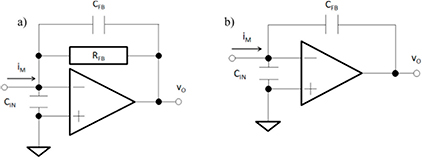
Figure 1. CVC topologies: transimpedance (a) integrator (PCI) architecture (b).
Download figure:
Standard image High-resolution imageThe transimpedance amplifier (figure 1(a)) is more common of the two presented systems, especially in the STM and C-AFM applications. This is the well understood architecture, however, there are several drawbacks associated with it, such as:
- The resistor in the feedback loop is the main source of noise of the transimpedance amplifier [16]. The resistor current noise decreases with the increase in resistance, therefore high value resistor in the feedback loop must be used in order to resolve currents at picoampere range so that the influence of the noise stemming from the feedback resistor is reduced and in order to achieve high enough CVC gain. Resistor meeting those criteria is usually large and difficult to be integrated with printed circuit board (PCB) as well as requiring special measures to preserve its parameters.
- Basic transimpedance amplifier can only effectively cover one or two decades of input current [3]. This translates into poor dynamic range, unless range switching selectors are employed what further increases the complexity of the circuit.
- The parasitic capacitance of the resistor in the feedback loop greatly limits the bandwidth of the CVC. In addition, the input capacitance can lead to oscillations of the circuit because of phenomena called gain-peaking. To counter this adverse effect a controlled capacitance needs to be introduced into the feedback loop. Unfortunately, this reduces the bandwidth even further. The described effect can be compensated for, but at the cost of increasing complexity by adding gain recovery circuitry [17].
- Noise floor of the transimpedance amplifier increases with the increase of its input capacitance [16]. This is related to the already mentioned gain-peaking effect and can greatly degrade the performance of the STM/C-AFM if a probe with too high capacitance is chosen to conduct the measurement as it will lead to deterioration of the resolution of the whole system.
The disadvantages of the transimpedance amplifier make it extremely difficult to design a circuit that would meet all requirements put forward for the PCI. This is the reason why an integrating amplifier (figure 1(b)), which most common application is the photocurrent measurement [18–20], should be also taken into consideration in the precise SPM current measurement. The described architecture is often used in high precision electrometers [21], therefore it should be ideally suited for the role envisioned for the PCI. As can be seen in figure 1(b), the capacitor replaces the resistor in the feedback loop. During the measurement, the measured current (im) flows through the capacitor what results in a change in output voltage (vo) as the capacitor is charged or discharged. This behaviour may be evaluated using equation:
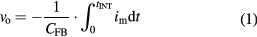
where: vo—output voltage, im—input current, CFB—feedback capacitance, tINT—integration time. As can be seen from (1), the gain of the circuit depends on both the feedback capacitance and the integration time. It is also important to mention, that in practical applications integrator circuit contains additional switches responsible for discharging the capacitor and preventing the saturation of the op-amp. This switched integrator behaves like a sampling system. Thus the signal acquisition is not continuous but proceeds in three steps:
- Sample—when vo follows the relation described by equation (1).
- Hold—when input is disconnected from the switched integrator. In this step it is possible to read-out vo value as it remains constant except for leakage and other parasitic effects.
- Reset—when the vo value is reset to default value (usually 0 V).
In comparison with the transimpedance amplifier, the switched integrator amplifier offers the following benefits [16]:
- A capacitor is not the source of the thermal noise. That removes the limit imposed by the Johnson noise of the resistor on the resolution of traditional transimpedance amplifier. The effect of the reset noise, caused by the thermal noise of the capacitor resetting circuitry resistance may be minimized using the Correlated Double Sampling technique [22, 23].
- The gain of the switched integrator circuit is dependent on the integration time. Therefore varying the integration time one can adjust the gain, thus a higher dynamic range with the same feedback element can be achieved.
- The effect of input capacitance on the noise floor is minimised because of using capacitors with relatively large (compared with the transimpedance amplifier topology) capacitance in the feedback loop.
For better understanding of the influence of the input capacitance on the performance of both amplifiers, it is useful to analyse their high frequency noise gain, as the high frequency noise is the dominant component for both amplifiers. This effect can be evaluated by using the following equation [16, 24]:
where: eout—the noise present at the output of the amplifier, ein—the noise present at the input of the amplifier, CIN—the input capacitance, CFB—the capacitance in the feedback loop. As has already been mentioned, the CFB is usually larger for the integrator amplifier than it is for the transimpedance one. The consequence of this is that the integrator exhibits lower noise gain for the same input capacitance when compared with its transimpedance counterpart.
In this paper, we describe the architecture and properties of PCI system that consists of electronic circuitry and dedicated software. Then, we present results of measurements, conducted with the PCI prototype. Their purpose was to determine the performance of the module, in terms of sensitivity and resolution, and to demonstrate its successful integration into the ARMscope SPM platform developed in-house at the Nanometrology Group. The big advantage of the proposed design is that the current flows through the tip only when the structure is biased. In this way the tip wear as well as unwanted surface modification possibility is reduced. It should be also mentioned, that the design is flexible enough to allow integration with almost every SPM machine.
2. Precise current integrator design
The current to voltage conversion in PCI is carried out with Texas Instruments' DDC112 integrated circuit. It contains two current measuring channels each consisting of a dual-switched integrator amplifier (figure 2) paired with a Σ▵ analogue to digital converter (ADC) [25, 26]. The dual switched integrator architecture makes it possible to integrate continuously the input current, as both integrators can operate in hold and reset phase alternatively.
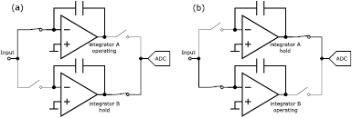
Figure 2. Simplified diagram of dual switched integrator at the input of DDC112 showing two alternating operating and hold phases (a) and (b) of integrators [27].
Download figure:
Standard image High-resolution imageThe ADC converts the output voltage of the integrator in hold phase. Since two integrators are feeding data for the same channel, offset mismatch between them is unavoidable and results in unwanted discrete frequency components in the signal spectrum. To prevent this from happening, digital offset correction is used. The immediate conversion of data into digital domain greatly reduces the number of additional components needed to be integrated in the module what, in turn, allows for small dimensions of the PCB.
The integration process is controlled by the CONV pin of DDC112 chip. Logical state at this pin (logical '1' or '0') determines which integrator (Side A or Side B) is acquiring the signal, and its duration determines the integration time. Each integrator contains its own set of capacitors whose values range from 12.5 pF to 87.5 pF in 12.5 pF steps. The full-scale current range of DDC112 depends on the value of integrating capacitor, integration time and reference voltage and is given by the following equation:
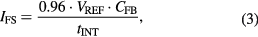
where:
- IFS—the full-scale current (A)
- VREF—the voltage reference (set at 4.096 V in the PCI)
- CFB—the capacitance of chosen integration capacitor (F)
- tINT—the integration time (s)
It is worth noting, that the full scale current of the DDC112 exhibits remarkablethermal stability, typically 25 ppm °C−1 [20], which causes that its influence on the total thermal drift during the warming-up phase of the C-AFM system is negligibly small [28]. Table 1 provides example of the full-scale PCI output for given integration time and capacitance as well as expected the best case noise values calculated in accordance with the datasheet of DDC112 chip.
Table 1. Example values of PCI full-scale range and corresponding best case noise values.
| tINT (ms) | fBW (Hz) | CFB (pF) | VREF (V) | IFS (nA) | ePPM (ppm of FS) | eRMS (fA) | eDEN (fA (√Hz)−1) |
|---|---|---|---|---|---|---|---|
| 0.5 | 1000 | 12.5 | 4.096 | 98.30 | 5 | 492 | 15.5 |
| 5 | 100 | 9.83 | 49.2 | 4.92 | |||
| 50 | 10 | 0.983 | 4.92 | 1.55 | |||
| 500 | 1 | 0.098 | 0.492 | 0.492 | |||
| 0.5 | 1000 | 87.5 | 688 | 3440 | 109 | ||
| 5 | 100 | 68.8 | 344 | 34.4 | |||
| 50 | 10 | 6.88 | 34.4 | 10.9 | |||
| 500 | 1 | 0.668 | 3.44 | 3.44 |
Note: tINT—integration time. fBW—bandwidth for given integration time. CFB—capacitance in the feedback loop of the amplifier, VREF—reference voltage, IFS—full-scale current, ePPM—noise value relative to IFS, eRMS—rms current noise value, eDEN—current noise density.
To provide all necessary signals for correct operation of DDC112 chip, as well as communication with other devices, a 32 bit microcontroller (µC) based on ARM CORTEX-M4 core with dedicated floating point unit (FPU) was used (STM32F405RG). The described microcontroller was selected against simpler microcontrollers for the following reasons:
- It is capable of generating all clock signals for the ADC in hardware while meeting necessary requirements regarding synchronization between main clock and CONV signal. The precise synchronization is necessary to minimize the digital noise coupled into integrators. The main clock frequency is 10 MHz, what allows for adjustment of the CONV signal in 100 ns steps.
- It has relatively large on-chip memory which allows to collect sufficiently long records before sending them to the host system. This is done in order to minimize digital activity on the board that is asynchronous with the operation of DDC112 chip.
- The on-chip FPU makes it possible to handle all operations on acquired data on the PCI board within reasonable amount of time. This frees the host from the need to allocate resources for data conversion, offset correction and averaging. The presence of FPU unit ensures that, the functionality of the PCI can be expanded by adding further signal processing functions via firmware modifications if the need arises.
Additionally, Analog Devices Dual Channel Digital IsolatorADUM1281 was applied to provide galvanic separation between the PCI and host device (ARMscope AFM system or personal computer) connected with USART interface. The block diagram of the PCI and its integration with in-house developed ARMscope system is shown in figure 3.
Figure 3. Block diagram of the designed PCI and its integration with in-house developed ARMscope system.
Download figure:
Standard image High-resolution imageThe entire PCI module was fabricated using 4-layer PCB that measured 7 cm per 5 cm. The board was split into analogue and digital parts using separate grounds connected together near DDC112 chip. Coupling of digital noise into analogue was minimized by proper signal layout. Figure 4 presents images of the fabricated prototype.
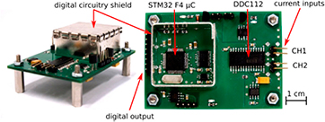
Figure 4. Image of the prototyped PCI module: (a) side view (b) top view.
Download figure:
Standard image High-resolution imageThe µC firmware was responsible for controlling the DDC112 and data acquisition according to the commands sent from the host. Also the ARMscope system firmware had to be enhanced to allow the integration with the proposed PCI.
Additionally a LabVIEW application for a personal computer (PC) was developed in order to perform tests of the designed and fabricated PCI module. The application supports full functionality of the device, making it possible to use the PCI as the standalone current measuring device. Moreover, the additional functions implemented in the application allow for analysis of basic parameters of measured signals. The most important among them is the capability to perform power spectral density (PSD) analysis, from here on referred to as current spectral density (CSD) because of the focus of the analysis on current noise distribution. The averaging method used in calculation of the spectrum is time interval square amplitude (TISA) with user-selectable windowing function.
3. Precise current integrator performance tests
The PCI was thoroughly tested in order to evaluate its performance as well as to ensure faultless cooperation with ARMscope controller. The results of PCI evaluation are presented in sections 3.1 and 3.2. The exemplary images obtained with C-AFM using PCI module are shown in section 3.3. In addition, the PCI performance was compared with the linear current amplifiers for informative purposes and the results of the comparison are discussed in section 3.4.
All the shown CSD spectra presented below were obtained by averaging 10 measurements series, where each series consisted of 2048 samples. The resulted spectra were further processed with averaging filter in order to smooth the shapes of the recorded curves.
3.1. PCI noise floor evaluation
The noise floor of the designed PCI was evaluated by taking the measurements with its inputs opened. Due to the PCI extreme sensitivity, all measurements had to be performed with the device carefully shielded from any electromagnetic interference.
For the measurements, the largest and the smallest possible feedback capacitance of 12.5 pF and 87.5 pF were used. Integration times for the measurements were chosen as multiples of 0.5 ms. Results for 20 ms integration time were interesting because they allow for the rejection of power line frequency (50 Hz) interference which is among the greatest troublemakers when it comes to measurements of low-level currents.
Figures 5 and 6 show exemplary CSD results. The lack of distinguishable discrete frequency components in the presented spectral density plots proves that the results are not affected by noise associated with power line or clock signal interference. It may be observed that in each case the lower value of feedback capacitance CFB results in lower noise density. That relation will hold true always when noise densities are compared for the same integration time, because bigger capacitance results in bigger full-scale measurement range (IFS). A noteworthy fact is that for the same IFS the larger feedback capacitance will correspond to lower overall noise, as can be seen from equation (1).

Figure 5. CSD measurement for integration time tINT = 50 ms.
Download figure:
Standard image High-resolution image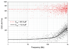
Figure 6. CSD measurement for integration time tINT = 500 µs.
Download figure:
Standard image High-resolution imageIt is also important to notice that the noise floor is not flat for the entire spectrum for the lower value of the feedback capacitor. This is the consequence of the module's input capacitance that comes from the DDC112 chip and the applied PCB. Numerical results of the discussed measurements were collected in table 2. Basing on these values it can be seen that the noise parameters of the designed module depend on the PCI settings, which is the value of both integration time tINT and feedback capacitance CFB. Therefore, it is possible to configure them to fit a specific application as needed.
Table 2. PCI noise floor specifications for selected integration times.
| tINT (ms) | CFB (pF) | IFS (nA) | fs (Hz) | eRMS (fA) | ePPM (ppm IFS) | eDEN (fA (√Hz)−1) |
|---|---|---|---|---|---|---|
| 0.5 | 12.5 | 98.30 | 2000 | 602.3 | 6.1 | 18.3 |
| 87.5 | 688.13 | 2150.0 | 3.1 | 67.0 | ||
| 5 | 12.5 | 9.83 | 200 | 61.8 | 6.3 | 5.7 |
| 87.5 | 68.81 | 215.3 | 3.1 | 21.4 | ||
| 20 | 12.5 | 2.46 | 50 | 16.1 | 6.6 | 3.2 |
| 87.5 | 17.20 | 54.9 | 3.2 | 10.8 | ||
| 50 | 12.5 | 0.98 | 20 | 7.4 | 7.5 | 2.3 |
| 87.5 | 6.88 | 22.6 | 3.3 | 7.0 | ||
Note: tINT—integration time. fs—sampling frequency for given integration time. CFB—capacitance in the feedback loop of the amplifier, IFS—full-scale current, ePPM—noise value relative to IFS, eRMS—rms current noise value, eDEN—current noise density.
In order to investigate the influence of the input capacitance on the measured noise parameters a further series of additional measurements was carried out. The results can be seen in figure 7.
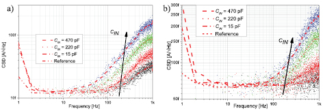
Figure 7. Input capacitance influence on the noise floor of the designed PCI: (a) CFB = 12.5 pF (b) CFB = 87.5 pF.
Download figure:
Standard image High-resolution imageThe influence of input capacitance on the PCI noise floor is shown quantitatively in table 3, which contains noise values relative to full scale for given CFB, integration time tINT and input capacitance CIN values. In agreement with equation (1) the lower feedback capacitance results in greater increase in noise than the bigger capacitance. It is also important to note that in the transimpedance amplifiers the typical value of CFB is kept much lower than even the lowest value the PCI is equipped with (for example the amplifier constructed by Carla et al [17] uses only 0.1 pF in its feedback loop). Therefore, we deduce that for the transimpedance amplifiers the influence of input capacitance is more pronounced. The reference value shown in the graphs and in the table 3 is the open input measurement, similar to those shown in figures 5 and 6.
Table 3. Influence of input capacitance on the device's noise floor for integration time 500 µs.
| CIN (pF) | e12 (ppm IFS) | e87 (ppm IFS) |
|---|---|---|
| Reference | 6.12 | 3.20 |
| 15.00 | 11.66 | 3.72 |
| 220.00 | 21.12 | 5.71 |
| 470.00 | 34.62 | 8.21 |
Note: CIN—input capacitance, e12—noise relative to IFS for CFB = 12.5 pF, e87—noise relative to IFS for CFB = 87.5 pF.
3.2. Exemplary current measurement
To demonstrate the possibility of using PCI in the femtoampere—range current measurements the differentiating low current source was used. It was developed alongside the PCI for the purpose of its characterization. It was similar to devices described by van-der-Brom [29] and Tauscher [30]. In it, the current generated using Agilent 33220A function generator with 10 MΩ series resistor was integrated at a Texas Instruments ACF 2101 low noise integrator with 470 nF integrating capacitor. The output voltage of the integrator was differentiated using 2.2 pF capacitor. For the measurement both PCI and the current source were placed in shielded box to avoid any electromagnetic interference.
Differentiating current source was excited with 50 mV, 20 mHz voltage from the function generator. Basing on the values of used components the amplitude of generated current should be 23.4 fA however, any parasitic capacitance parallel to the differentiating capacitor will increase its value. The PCI settings were chosen as follows: CFB = 87.5 pF and tINT = 500 ms in which case the full scale current was IFS = 0.668 nA. The result of the sinusoidal current measurement is presented in figure 8. As can be seen the signal with amplitude of approximately 28 fA was successfully measured, which was 24 ppm of the IFS.

Figure 8. Example measurement of sinusoidal signal.
Download figure:
Standard image High-resolution image3.3. C-AFM experiments using PCI
In order to test how the designed PCI operates with the with ARMscope SPM scanning controller, a series of test measurements was conducted using C-AFM mode, with the PCI module used as the current sensing transducer. Two types of structures were measured: highly organized pyrolytic graphite (HOPG, figure 9) and graphene obtained using CVD methods on 6H–SiC substrate [31] (figure 10).
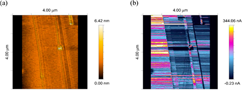
Figure 9. AFM and C-AFM Measurement on HOPG substrate: (a) topography image, (b) current image.
Download figure:
Standard image High-resolution image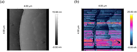
Figure 10. AFM and C-AFM measurement of SiC/graphene sample: (a) topography image, (b) current image.
Download figure:
Standard image High-resolution image
For both samples topography and current images were recorded. For all measurements CFB was set to 87.5 pF and integration time was chosen to be 1 ms. The load force of probe on the surface was estimated to be ~40 nN. For the HOPG measurement the sample was biased with 50 mV. It should be noticed that the recorded topography image agrees with obtained current image. In places where the IFS value was reached there is a possibility that the regulator did not maintain the constant force between the sample and the tip that might have resulted in increase of current. The local contamination of the sample is also a possibility and change of the tunnelling current collected by the conductive tip.
In case of graphene measurement the sample bias was set at 15 mV. It can be seen that the topography image of the sample contains less information than the current image, which shows the strength of combining two imagining modes in one C-AFM instrument.
Both the performed tests clearly show that the PCI integration with the SPM controller was done correctly and the quality of the obtained images is satisfactory.
3.4. Comparison with linear current amplifiers
The performance of the designed PCI, which was shown in previous sections, was compared to the data available from the leading manufacturers of STM/C-AFM commercial systems. Parameters of the CVCs in three commercially available systems were shown in table 4. As no precise and explicit information about the bandwidth of their instruments was given in the available documentation, only their measurement range and resolution were evaluated.
Table 4. Comparison of current measurement capabilities of various STM/C-AFM instruments [32, 33].
| Instrument | Measurement range (pA) | Resolution (fArms) |
|---|---|---|
| #1 | 0.06–100.00 | 50.0 |
| #2 | 1.00–100 000.00 | 1000.0 |
| #3 | 1.0–20 000.00 | 500.0 |
Quick glance at the table 4 reveals that the PCI module can be easily tuned to match or outmatch commercial instruments in certain situations (please, consult table 2 for specific values). However, it has to be noted that there always will be the bandwidth—resolution tradeoff and the improvement of one of these parameters will cause the decline of the other.
Moreover, the great configurability of the designed module allows the user to apply settings that are an ideal match for a given task or perform complex measurements without disturbing the measurement setup as the tuning is done in software on a level that is not available for the traditional CVC devices. Typically the transimpedance CVCs contain, at best, only a limited number of discrete fixed gains while the current to voltage conversion factor in the PCI may be set precisely by changing both the integration time and feedback capacitance.
The concept of the integrating amplifier may also be useful in case of multi-channel applications in which the lack of bulky, high value resistors is extremely convenient. The serious limitation for transimpedance amplifiers may be the sheer size of such system. For example, the dimensions of a 128-channel picoammeter [34], built as a transimpedance amplifier, may be impractical in some applications, for example in multi-cantilever AFM system. On the other hand the PCI module of similar capabilities can be easily scaled to offer similar channel count by replacing the DDC112 with its 128-channel counterpart DDC1128 on a PCB that is only slightly larger than the discussed module.
4. Summary
A complete CVC module for SPM microscopy was described in this paper. Owing to the integrator topology, the device offers unmatched configurability, with a possibility of fine-tuning the PCI on-the-fly to the task-at-hand. Depending on easily configurable parameters it is possible to obtain for example the 2.15 pA resolution at 688 nA range with 1 kHz bandwidth or 7.4 fA resolution at 0.98 nA range with 10 Hz bandwidth. The measurement of sinusoidal current with 28 fA amplitude was presented. The performance of the device is comparable to the leading commercial systems and is further enhanced by auto-calibration function and fully digital output. The latter eases the integration of the module into the C-AFM/STM system, as a simple serial interface is all that is needed to communicate both devices. The usage of powerful microcontroller makes it possible to integrate additional digital signal processing (DSP) features on-chip without adverse effects on the host system. All this functionality is contained on a small PCB, that is easier to place closer to the sample, what further reduces measurements errors. In addition, the PCI module demonstrates great potential for multi-channel measurements in cooperation with cantilever arrays. In this way, the bandwidth limitations of the module can be leveraged. Finally, all the described features of the discussed device make it suitable for other uses than SPM. The dielectric response measurements are one of many possible applications where the wide dynamic range and low-current detection capability of the PCI could be used.
Acknowledgments
The research presented in this paper was supported by the Foundation for Polish Science TEAM Programme (Grant No. TEAM/2012-9/3), co-financed by the European Regional Development Fund resources, the European Commission under grant (FP7 STREP) NANOHEAT—MultidomaiN plAtform for iNtegrated MOre-tHan-MoorE/Beyond CMOS systems charActerisation & diagnosTics, grant no. 318625 and Wrocław University of Technology statutory grant (S50037).