

Abstract
Based on first-principles, we conducted an in-depth study of the GeC/InS van der Waals heterostructure formed by GeC and InS and discussed its structure, electronic properties and optical properties. First, we observe that this heterostructure has negative binding energy, indicating that the interlayer interactions are mainly affected by van der Waals forces. Through band structure and density of state analysis, we confirmed its type-II band alignment characteristics, which means that photogenerated carriers have the ability to automatically separate in space. Moreover, the average charge density difference and Bader charge analysis show that there is a built-in electric field in the heterostructure, and further proves that GeC/InS forms a Z-scheme charge transfer mechanism. Interestingly, the band edge position spans the water redox potential and can fully induce the redox reaction of water splitting, indicating that it is a potential photocatalyst. The high light absorption coefficient shown in the absorption spectrum also further confirms its excellent photocatalytic activity. The most striking thing is that the solar hydrogen production efficiency of GeC/InS heterostructure is as high as 44.39%. Our research demonstrates the theoretical basis for GeC/InS heterostructure as a photocatalyst.
Export citation and abstract BibTeX RIS
1. Introduction
Photocatalytic water splitting is a promising clean energy production technology. Since Fujishima et al successfully achieved photocatalytic decomposition of water on a titanium dioxide semiconductor electrode for the first time in 1927 [1], research on improving the efficiency of photocatalysts has become crucial. Many semiconductor materials have high hopes as potential photocatalysts, but they face some challenges, such as wide band gaps, rapid recombination of photogenerated carriers, low light absorption efficiency, and low photocatalytic activity, which significantly reduce their water decomposition efficiency [2]. Therefore, nano-structuring the material by adjusting its size and shape is a possible solution. As an illustration, there has been considerable interest in the exceptional photocatalytic characteristics of two-dimensional materials (2D) [3]. These 2D photocatalytic materials have high specific surface areas, which help to accelerate the adsorption of reactants, thereby promoting photocatalytic reactions [4]. Among them, heterostructures constructed from different 2D materials have attracted much attention due to their excellent optical absorption properties, good carrier separation effect, and excellent photocatalytic performance [5–9]. Compared with 2D single-layer semiconductors, direct Z-scheme heterostructures that simulate natural photosynthesis have many advantages and have been extensively studied in recent years [10, 11]. The direct Z-scheme heterostructure has strong redox ability and can catalyze the evolution reaction of hydrogen and oxygen on the surface of different materials, thereby effectively improving the photocatalytic efficiency [12–16]. Its simple structure also makes it easy to prepare experimentally, so it has a wide range of applications in different fields [17–19].
As a member of the main group IV compound, 2D germanium carbide (GeC) semiconductor with a graphene-like structure exhibits excellent electronic, structural, mechanical, magnetic and optical properties [20–23]. Single-layer GeC has a relatively large direct band gap and excellent semiconductor properties, so it can be used to design new nanoscale electronic devices. Recently, a single-layer two-dimensional GeC material was successfully synthesized experimentally [24], and it showed a stable structure [25, 26]. However, the valence band maximum (VBM) of GeC is unable to cross the potential of the oxygen evolution reaction (OER) and thus cannot be used for photocatalytic OER. Nonetheless, theoretically, research on controlling the band edge position of GeC by constructing heterostructures to achieve photocatalytic water splitting is still full of potential. Zhang et al used first-principles calculations to analyse the water decomposition performance of GeC/HfS2 heterostructures and found that they possessed outstanding visible light absorption performance and carrier mobility, and achieved overall photocatalytic water spontaneous decomposition under neutral conditions [27]. In addition, there are other studies on constructing GeC heterostructures for photocatalytic water splitting, such as GaN/GeC, GeC/SnSSe, GeC/BSe, GeC/ZnTe and GeC/ZnO [28–32].
At the same time, InS, as an In-based semiconductor, belongs to the III–VI group and is one of the typical representatives [33, 34]. In and S atoms are arranged into an S–In–S structure, and the layers are connected through van der Waals forces. It has excellent photo-responsive characteristics, and its single layer has an indirect band gap of 2.73 eV [35]. In the experiment, a single layer of InS was successfully synthesized, and its structure is similar to that of a single layer of InSe. However, its light absorption performance in the visible range still has certain deficiencies. Therefore, by constructing a heterostructure method, we can effectively make up for the shortcomings of the single-layer material itself that is difficult to control. In order to facilitate the preparation of efficient semiconductor catalysts, one can consider using an InS monolayer as the substrate and selecting another semiconductor material to jointly construct a heterostructure. Zhang et al and their research team calculated P-doped Type-II GaSe/InS heterostructures and found that the P-GaSe/InS heterostructures are capable of spontaneous thermodynamic overall water splitting under acidic conditions [36]. Considering that GeC and InS single-layer materials have been successfully synthesized, there is good reason to believe that the GeC/InS heterostructure may be successfully constructed in future experimental studies and exhibit excellent optoelectronic properties.
In summary, our objective is to combine GeC and InS to create a GeC/InS heterostructure tailored for the photocatalytic water splitting process. We conducted comprehensive first-principles calculations to evaluate the heterostructure's electronic and optical properties. To become an efficient photocatalyst, the heterostructure must have appropriate band gap values, conduction band minimum (CBM) and VBM, and the GeC/InS heterostructure satisfies this requirement well. As a type-II energy band alignment, this heterostructure can separate photogenerated electrons and holes in space, allowing hydrogen and oxygen production reactions to occur on different sides. The presence of a built-in electric field (Eint) and energy band bending promotes a Z-scheme electron transfer mechanism, enhancing the separation of photogenerated carriers. Moreover, the higher light absorption coefficient and solar-to-hydrogen (STH) efficiency indicate that the GeC/InS heterostructure can be used as a photocatalyst for water splitting.
2. Calculation method
In this article, we use the Vienna Ab initio Simulation Package for material property calculations. We applied first-principles of density functional theory and performed all energy calculations and geometry optimization using the Perdew–Burke–Ernzerhof (PBE) pseudopotential [37]. The exchange correlation potential is represented by the generalized gradient approximation associated with the PBE functional [38]. To obtain more accurate results, we employ the HSE06 function in all electronic and optical calculations [39]. In the calculations, we adopted a plane wave cut-off energy of 450 eV and a 6 × 6 × 1 setting for Brillouin zone sampling. In order to accurately describe the weak van der Waals interaction force between GeC and InS, we used Grimme's DFT-D3 method [40]. Furthermore, we introduced a vacuum layer of 20 Å to prevent interactions in the periodic structure [41]. During the atomic relaxation process, we set the convergence standards of energy and force as 1 × 10⁻⁵ eV and 0.01 eV Å−1 respectively, and ensured that each atom in the system was fully relaxed. To study the thermal stability of the GeC/InS heterostructure, we performed ab initio molecular dynamics (AIMD) simulations, during which the temperature condition of 300 K was explored. The total time of our simulation is 6 picoseconds (ps) and a Nose–Hoover thermostat regularization system is used for temperature control [42, 43].
3. Results and discussion
3.1. Structural optimization and electronic properties
Before studying the GeC/InS heterostructure, we first discussed the structure and properties of single-layer GeC and InS in detail to verify the accuracy of the calculation method we used. The lattice constants of unit cells GeC and InS are 3.23 eV and 3.91 Å respectively after optimization, which is consistent with previous research results [44–46]. In order to meet the requirements of the lattice mismatch degree of the heterostructure, we expanded the unit cell GeC by 2 × 2 and InS by √3 × √3. Figures 1(a) and (b) show the fully optimized geometries of a 2 × 2 × 1 GeC monolayer and a √3 × √3 × 1 InS monolayer, with lattice constants of 6.55 Å and 6.77 Å, respectively, which are honeycomb structures. During the structure optimization process, the Ge–C bond length was tuned to 1.88 Å for GeC and 2.56 Å for In–S and 2.80 Å for In–In in InS, and these values are in agreement with the results of previous studies [44, 45]. By using the HSE06 functional, we obtained the energy band diagrams (c) and (d), indicating that GeC and InS belong to semiconductor materials with band gaps of 2.89 eV and 2.66 eV, respectively. These results are consistent with the findings of other researchers and further demonstrate the reliability of our computational approach [45, 47]. In the Brillouin zone, the former is a direct band gap where both the CBM and the VBM are located at the high-symmetry K point, and the latter is an indirect band gap where the CBM and the VBM are located at the high-symmetry Г and K–Г points, respectively.
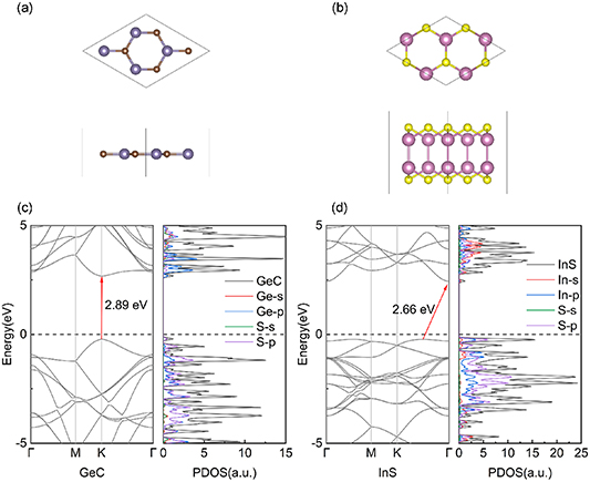
Figure 1. (a) Top view and side view of GeC monolayer, (b) top view and side view of InS monolayer, where Ge, C, In, and S atoms are represented by purple, brown, pink, and yellow balls respectively. Band structure and projected state density of (c) GeC monolayer and (d) InS monolayer.
Download figure:
Standard image High-resolution imageThe heterostructure is formed by vertically stacking two single-layer materials, and its lattice mismatch needs to be within 5% to form a stable state. The lattice constant of GeC is 6.55 Å, while that of InS is 6.77 Å, resulting in a mismatch of only about 3.2%, indicating that heterostructures of GeC and InS can be successfully prepared experimentally. After optimization, the geometric structure of the heterostructure is shown in figure 2(a), with a lattice constant of 6.59 Å and a layer spacing of 3.51 Å. In the heterostructure, the Ge–C bond length is 1.90 Å, the In–S bond length is 2.53 Å, and the In–In bond length is 2.79 Å. After analysis, we found that the interatomic bond lengths changed very little before and after the formation of the heterostructure, indicating that almost no atomic rearrangement occurred, thanks to the small lattice mismatch. Binding energy is a key parameter to evaluate the thermodynamic stability of the system. For GeC/InS heterostructure, we can use the following formula to calculate the binding energy:


Figure 2. (a) Top view and side view of GeC/InS, (b) relationship between binding energy and layer spacing, the dotted line represents the interlayer distance at the equilibrium position, (c) GeC/InS heterostructure at 300 K under continuous 6 ps AIMD simulation temperature and energy changes. The inset shows the initial and final structures in AIMD simulations.
Download figure:
Standard image High-resolution imageIn the above formula, Eb represents the binding energy, EGeC/InS, EGeC and EInS represent the total energy of the heterostructure GeC/InS, GeC and InS respectively. In the definition of binding energy, negative values indicate the stability of the structure, and the smaller the value, the more stable it is. The binding energy of the GeC/InS heterostructure is calculated by formula (1) to be equal to −0.39 eV, which is similar to the binding energy of other heterostructures g-C3N4/SnS2 and HfS2/SiSe [48, 49]. It shows that there is a stable interaction in the heterostructure, and this effect is the weak van der Waals force. In addition, vertical strain can be used to tune the electronic properties of the heterostructure, so we tried to introduce vertical strain by adjusting the distance between the GeC and InS layers. Generally speaking, heterostructures with different layer spacing have different stabilities. As shown in figure 2(b), when the layer spacing is 3.51 Å, the binding energy is the smallest, that is, the stability is the highest. Whether the layer spacing is gradually increased or decreased, the binding energy gradually increases, that is, the stability decreases. Especially when the layer spacing decreases to 2.81 Å, the binding energy becomes positive, indicating that the heterostructure is no longer stable. Therefore, we selected a heterostructure with a layer spacing of 3.51 Å for subsequent studies, which is consistent with the optimization results. To further prove the stability of this structure, we calculated its phonon spectrum. The results are shown in figure S1. The absence of negative values indicates that the GeC/InS heterostructure is stable. In order to verify the thermodynamic stability of the GeC/InS heterostructure, we performed AIMD calculations and constructed a 2 × 2 GeC/InS supercell, as shown in figure 2(c). The energy and temperature eventually stabilize throughout the process, and the interpolated plots show that the heterostructure shows no obvious structural distortion after 6 ps of 300 K simulation, which further proves that the GeC/InS heterostructure is dynamically stable.
In figure 3(a), the energy band structure of the GeC/InS heterostructure is depicted. Our calculations reveal an indirect band gap of 1.54 eV for the heterostructure. The band gap is smaller than that of single-layer GeC and InS, which means that electrons can more easily cross the band gap from the valence band (VB) to the conduction band (CB) to form free electrons. After comparing with the band structure of the single-layer material (figures 1(c) and (d)), we found that the CB of the GeC/InS heterostructure is closest to that of InS, while the VB is similar to that of GeC. This can be attributed to the smaller lattice mismatch in the heterostructure and the weakening of van der Waals interactions. The GeC/InS heterostructure displays an indirect band gap of 1.54 eV, with the band gap extending from the blue K point at the VBM to the orange Г point at the CBM. Subsequently, we conducted an analysis of the heterostructure's partial wave state density, as illustrated in figure 3(b). Notably, the CBM primarily comprises InS, while GeC significantly contributes to the VBM. This is consistent with the comparison results of the band structure diagrams, indicating that the heterostructure has a typical type-II band alignment. For the GeC monolayer, the states in CBM and VBM are dominated by Ge-p and C-p orbitals together. In a single layer of InS, the contribution to the CBM state primarily arises from In-s and S-p orbitals, whereas the VBM state results from In-p and S-p orbitals. Consequently, upon the formation of the heterostructure, the CBM state predominantly comprises In-s and S-p orbitals, while GeC significantly contributes to the VBM state through its C-p orbitals. This result is also clearly reflected in figure 3(b). Therefore, by combining these two single-layer materials to form a heterostructure, their respective properties are well preserved. The band structure of the heterostructure indicates the existence of type-II band alignment, which means that the GeC/InS heterostructure has potential application prospects in optoelectronic devices.
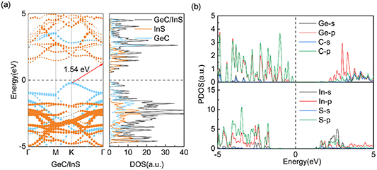
Figure 3. (a) Projected band structure and projected density of states of GeC/InS heterostructure, (b) partial density of states of GeC/InS heterostructure.
Download figure:
Standard image High-resolution image3.2. Z-scheme characteristics of GeC/InS heterostructure
The coupling between single layers will lead to the redistribution of charge at the heterostructure interface, and new electronic properties may appear. This phenomenon depends on the work function of the material, and is defined as follows:

Among them, Evac represents the vacuum energy level, and EF represents the Fermi energy level. Through calculation, we obtained that the work functions of single-layer GeC, InS and GeC/InS heterostructures are 5.12, 6.72 and 5.3 eV respectively, as shown in figure 4, which is basically consistent with previous research results [47]. When the GeC and InS monolayers are in contact, since the work function of the GeC monolayer is lower than that of the InS monolayer, the Fermi level of the GeC monolayer is higher than that of InS. This leads to an automatic transfer of electrons from the GeC monolayer to the InS monolayer on contact, so that the Fermi energy levels of GeC (InS) move down (up) until they reach the same position, giving the GeC/InS heterostructure a work function of 5.3 eV. Electrons accumulate in the InS monolayer, while holes accumulate in the GeC monolayer. This accumulation creates a built-in electric field directed from GeC to InS.
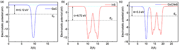
Figure 4. (a) Work function of single layer GeC and (b) InS, (c) work function of GeC/InS heterostructure. The light blue and black dashed lines represent the vacuum energy level and Fermi level respectively.
Download figure:
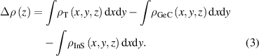
Standard image High-resolution imageDue to the charge rearrangement at the interface, the electronic properties of the heterostructure will be somewhat different from those of the original single layer. In order to see the charge distribution at the GeC/InS heterostructure interface in more detail, we calculated the average charge density difference Δρ(z) in the Z-axis direction through the formula [50, 51],
Among them,  ,
,  and
and  represent the charge density of GeC/InS heterostructure, single layer GeC and InS at point (x, y, z) respectively. It can be seen from figure 5(a) that there is a certain rearrangement of charges near the heterostructure interface. Generally speaking, electrons are concentrated in the InS layer and there is a certain amount of electron consumption on the GeC layer, which was visually observed through the 3D isosurface map. Figure 4(b) shows the electrostatic potential of the heterostructure in the Z-axis direction. It can be seen that there is a potential drop between the single layer GeC and InS. A large potential drop plays an important role in the separation of photoexcited electrons and holes. Bader charge analysis of the GeC/InS heterostructure is shown in figure 5(c). Compared with independent GeC monolayers and InS monolayers, the sum of electrons transferred by Ge and C atoms is 0.058e, while In and S atoms get 0.058e, indicating that 0.058e diffused from the GeC single layer to the InS layer. The specific electron transfer numbers are in figure S2.

Figure 5. (a) Average charge density difference along the Z-axis of a GeC/InS heterostructure, where blue colour represents electron depletion and yellow colour represents electron accumulation (3D plot of charge density difference at the time of insertion of the figure), (b) electrostatic potential of the heterostructure along the Z-axis, with the blue solid line and the red solid line contributed by GeC and InS, respectively. (c) Bader charge.
Download figure:
Standard image High-resolution imageIn order to use the GeC/InS heterostructure as a photocatalyst for water splitting, it is necessary to ensure that it has appropriate band gap and band edge positions to span the redox potential of water. According to the literature, we know that under vacuum conditions at pH = 0, the redox potential of water (EH+/H2/EO2/H2O) is −4.44 eV and −5.67 eV respectively (shown as the red dotted line in figure 6) [52]. To further evaluate the suitability of the GeC/InS heterostructure, we calculated EH+/H2 and EO2/H2O in the range of pH = 0–7, as shown in the following formulas:


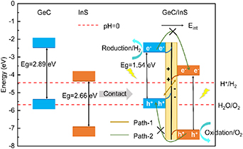
Figure 6. The band edge positions of the two monolayers of GeC and InS at the vacuum energy level and the band edge positions of the heterostructure after their contact. There are also built-in electric field directions and photogenerated carrier transfer paths in the heterostructure. The red dotted lines in the figure represent the redox potential of water when the pH is equal to 0 respectively.
Download figure:
Standard image High-resolution imageThe calculation results at different pH values show that as the pH value increases, the values of EH+/H2 and EO2/H2O also gradually increase. At a pH of 7, the EH+/H2 and EO2/H2O values stand at −4.03 eV and −5.26 eV, respectively. Figure 6 illustrates the band edge positions and band gaps, calculated with HSE06, for single-layer GeC, InS, and GeC/InS heterostructures. The staggered energy bands in the GeC/InS heterostructure on the right once again clearly prove that the heterostructure is a type-II band alignment. The CBM of GeC monolayer is higher than the reduction potential of H+/H2 (−4.44 eV), which is suitable for the reduction reaction of water splitting. The CBM and VBM of InS satisfy the band edge positions of the redox of water splitting.
Figure 6 further provides an illustrative depiction of the migration of photoexcited electron-hole pairs at the interface of the GeC/InS heterostructure. Since the work function of InS is higher than that of GeC, when they come into contact, electrons migrate from the GeC side to the InS side until the equilibrium state of the electron Fermi level is reached. This results in the formation of a space charge region at the GeC/InS heterostructure interface, which generates an electric field Eint in the direction from GeC to InS, consistent with the previous electron interlayer transfer. The existence of Eint causes the electrons in the space charge region to have additional potential energy at every point, causing the energy band near the interface to bend. As a consequence, the positive charges present on the InS side experience repulsion from the holes in GeC, resulting in a reduction of potential energy. This interaction causes the energy band of the InS layer to bend downward at the interface. Conversely, the potential energy of the GeC layer increases, causing its energy band to bend upward. When subjected to light, electrons within the VB of both GeC and InS get excited into their respective CB, generating photogenerated electrons and leaving photogenerated holes in the VB. Under the influence of Eint, these photogenerated electrons efficiently recombine with photogenerated holes within the VB of GeC (Path-1). Due to the influence of band bending, the electron flow from CB in GeC to CB of InS and the flow of holes from VB in InS layer to VB of GeC are hindered (Path-2 is blocked). Finally, the photogenerated electrons stay in the GeC layer, while the photogenerated holes accumulate in the InS layer, which helps to effectively separate the photogenerated electron-hole pairs. This direct Z-scheme transfer path promotes redox reactions between different layers: the hydrogen production reaction mainly occurs in the GeC layer, while the oxygen production reaction occurs in the InS layer. Therefore, the GeC/InS heterostructure has the potential to serve as a highly efficient photocatalyst.
3.3. Gibbs free energy change
In order to evaluate the photocatalytic activity of the GeC/InS van der Waals heterostructure, the intermediate reactants and Gibbs free energy of the HER and OER processes were calculated respectively. The HER process reaction is as follows:


Among them, * represents the active site on the GeC/InS heterostructure. From reaction equations (6) and (7), it can be concluded that the intermediate in the HER process is H*. We know that the necessary condition for becoming a high-efficiency hydrogen evolution photocatalyst is ΔGH ∼ 0 [53]. As shown in figure 7(a), the ΔGH of the GeC/InS van der Waals heterostructure is 0.35 eV. Therefore, this heterostructure is suitable as a HER photocatalyst. The most stable adsorption position of H* on the GeC/InS layer is shown in figure 7(c).
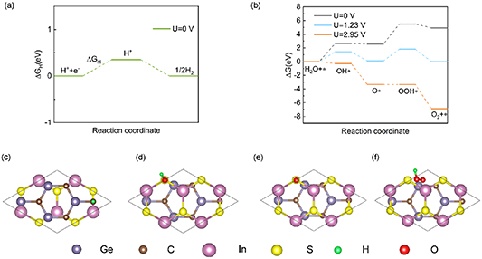
Figure 7. (a) Free energy steps of the reduction reaction of the GeC layer and (b) the oxidation reaction of the InS layer in the GeC/InS heterostructure, (c) H*, (d) OH*, (e) O*, (f) top view of the optimized structure of the OOH* intermediate.
Download figure:
Standard image High-resolution imageThe OER process is as follows (8)–(11):


Reaction equations (8)–(11) indicate that the intermediate products of the OER process are OH*, O* and OOH*. The calculated results of ΔGOH*, ΔGO* and ΔGOOH* of the GeC/InS van der Waals heterostructure are 2.67, 2.56, and 5.49 eV, as shown by the black line in figure 7(b). The third step has the largest free energy difference change of 2.94 eV, which is a potentially decisive step in the OER process. Under the external potential of U = 0 V and U = 1.23 V, the second and fourth steps decrease, and the remaining steps increase. Considering the maximum free energy difference, an appropriately increased external potential is needed to promote OER, so we explore the free energy change trend under an external potential of U = 2.95 eV. The orange line in figure 7(b) indicates that the free energy of all reaction steps shows a downward trend, which further illustrates that OER is an exothermic process under an applied potential of 2.95 eV.
3.4. Optical properties and energy conversion efficiency
Optical properties are an important indicator of photocatalyst performance, and light absorption coefficient is an important indicator of optical properties. The expression of light absorption coefficient α(ω) is [54],
Among them,  1(ω) and 2(ω) are the real part and imaginary part of the dielectric constant respectively, α, ω, and c are the absorption coefficient, angular frequency and speed of light under vacuum conditions, respectively [55, 56]. As shown in figure 8(a), we calculated the absorption spectra of the GeC layer, InS layer and GeC/InS heterostructure. Both single layers absorb visible light to a certain extent, and at 345 nm, the heterostructure light absorption reaches a maximum of 4.57 × 105 cm−1. The GeC/InS heterostructures exhibit a wider light absorption range, extending to 1000 nm. At this time, the GeC/InS heterostructure can absorb more visible light photon energy, which is related to the overlap of electronic states caused by the interlayer coupling of the two monolayers. As can be seen from figure 8(b), when +1% or +2% strain () is applied, the two absorption peaks have a certain red shift near visible light, indicating that more photons can be absorbed at this time; when strains of −1% and −2% are applied, the overall light absorption undergoes a blue shift, and the absorption peak near 472 nm increases to a certain extent, indicating that the light absorption capability has been enhanced to a certain extent. Therefore, applying strain to the GeC/InS heterostructure is an effective measure to change the light absorption capability.
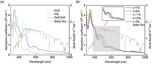
Figure 8. (a) Light absorption coefficients of GeC, InS and GeC/InS heterostructures. (b) Optical absorption coefficient of GeC/InS heterostructure under different .
Download figure:
Standard image High-resolution imageIn order to further quantify the photocatalytic efficiency of GeC/InS heterostructure. Using the approach developed by Fu et al [57], we performed calculations to determine the efficiency of STH conversion. The detailed calculation is as follows:

The calculation involved evaluating the light absorption efficiency (ηabs) and the carrier utilization efficiency (ηcu).
ηabs definition:
where P(hω) is the AM1.5G solar flux at the photon energy hω, Eg is the band gap of GeC/InS (1.54 eV),  is the total power density of incident simulated sunlight (AM1.5G),
  indicates the power density that can be absorbed by the GeC/InS heterostructure.
ηcu definition:
Among these parameters, ΔG represents a constant value of 1.23 eV, which signifies the potential difference required for water splitting. E corresponds to the photon energy that can effectively drive the water splitting process, while  denotes the effective photocurrent density. The value of E can be determined using the following formula:
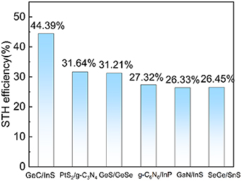
Among them, χ(H2) and χ(O2) are the potentials of hydrogen evolution and oxygen evolution respectively. It is calculated that χ(H2) = 1.937 eV and χ(O2) = 1.397 eV of GeC/InS, so Eg = 1.54 eV. The calculated STH conversion efficiency of the GeC/InS heterostructure is 44.39%. As shown in figure 9, compared with the heterostructures studied previously, the STH efficiency of GeC/InS is higher. For example, PtS2/g-C3N4 (31.64%) [58], GeS/GeSe (31.21%) [59], g-C6N6/InP (27.31%) [60], GaN/InS (26.33%) [45], SeGe/SnS (26.45%) [61].
Figure 9. (a) STH efficiency comparison of GeC/InS heterostructure and other heterostructure materials.
Download figure:
Standard image High-resolution image
4. Conclusion
As mentioned above, we theoretically studied the photocatalytic water splitting characteristics of GeC/InS heterostructure using first-principles. First, the binding energy calculation results show that the binding energy of the heterostructure is −0.39 eV, confirming the stability of its structure. From the perspective of electronic properties, the energy band diagram shows that the band gap of the heterostructure is 1.54 eV, and the density of states diagram shows that the energy band alignment belongs to type-II that can promote the separation of photogenerated carriers. Furthermore, the Z-scheme electron transport mechanism of the heterostructure receives additional substantiation from the results of average charge density difference and Bader charge analysis. In terms of photocatalytic water splitting reaction, free energy calculation results show that it helps to promote the water splitting reaction under light conditions. Simultaneously, the GeC/InS heterostructure exhibits strong light absorption characteristics, particularly noteworthy is the peak absorption coefficient at 345 nm, which reaches a maximum value of 4.57 × 105 cm−1 in the visible light range. Furthermore, the heterostructure's light absorption performance is enhanced under varying strains compared to its original configuration. Most importantly, the STH conversion efficiency of the GeC/InS heterostructure is as high as 44.39%. Taken together, these findings demonstrate that the GeC/InS heterostructure is an excellent photocatalyst candidate and provide a solid theoretical basis for future experiments.
Acknowledgments
This work was supported by the National Key R&D Program of China (2018YFB1600200), the Major Project of International Scientific and Technological Cooperation Plan in Shaanxi (2020KWZ-008), the Natural Science Foundation of Shaanxi Province (2021GY-255), and the Fundamental Research Funds for the Central Universities CHD (300102312401).
Data availability statement
All data that support the findings of this study are included within the article (and any supplementary files).
Supplementary data (0.2 MB PDF)