
Abstract
In the 60 years since the invention of the laser, the scientific community has developed numerous fields of research based on these bright, coherent light sources, including the areas of imaging, spectroscopy, materials processing and communications. Ultrafast spectroscopy and imaging techniques are at the forefront of research into the light–matter interaction at the shortest times accessible to experiments, ranging from a few attoseconds to nanoseconds. Light pulses provide a crucial probe of the dynamical motion of charges, spins, and atoms on picosecond, femtosecond, and down to attosecond timescales, none of which are accessible even with the fastest electronic devices. Furthermore, strong light pulses can drive materials into unusual phases, with exotic properties. In this roadmap we describe the current state-of-the-art in experimental and theoretical studies of condensed matter using ultrafast probes. In each contribution, the authors also use their extensive knowledge to highlight challenges and predict future trends.
Export citation and abstract BibTeX RIS

Original content from this work may be used under the terms of the Creative Commons Attribution 4.0 licence. Any further distribution of this work must maintain attribution to the author(s) and the title of the work, journal citation and DOI.
1. The 2021 roadmap for ultrafast probes of condensed matter
James Lloyd-Hughes1 and Peter Oppeneer2
1University of Warwick, United Kingdom
2Uppsala University, Sweden
1.1. Historical background
While the scientific and technological developments made by many researchers worldwide have contributed to the creation of ultrafast spectroscopy as a research field in its own right, the field can trace much of its origins to the seminal development of chirped pulse amplification (CPA) by Strickland and Mourou in 1985, for which they were awarded a share of the 2018 Nobel Prize in Physics. Indeed, as illustrated in figure 1, in the early 1990s journal articles featuring 'ultrafast spectroscopy' or 'femtosecond spectroscopy' as keywords started to appear, leading to the current >1500 publications per year. Although bright light sources at large-scale facilities have contributed significantly, it is the ready availability of high-power, tabletop lasers based on CPA that has underpinned the dramatic expansion of ultrafast spectroscopy witnessed over the last three decades. Both academia and industry have played critical roles in refining and improving such laser amplifiers, increasing their peak power and shortening their pulse duration, but also enhancing their reliability and introducing turn-key operation. Here, the academic community has undoubtedly benefited from the drive to improve the stability of CPA lasers for industrial applications, which include micro-machining and laser surgery.

Figure 1. Journal articles per year with 'spectroscopy' in the topic, plus 'attosecond' (blue) or 'femtosecond' (orange). Other articles with 'ultrafast' and 'spectroscopy' are also shown (green). Source: Web of Science.
Download figure:
Standard image High-resolution imageWhile the ultra-short duration of light pulses from CPA lasers allows pump-probe experiments to track dynamics on femtosecond to nanosecond timescales, it is the extreme peak intensity that is perhaps even more significant, as it has enabled the conversion of light from the laser's fundamental wavelength (often around 800 nm, 1064 nm or 1550 nm) to a wide range of the electromagnetic spectrum. Here, non-linear optical processes—like high harmonic generation (HHG), second harmonic generation, supercontinuum generation, difference frequency generation and optical rectification—are deployed with great effect to produce light pulses from XUV wavelengths (∼10–100 nm) through the visible all the way to the THz range (∼300 μm). This flexibility allows innumerable combinations for the excitation and probe sources, even for simpler two-beam pump-probe experiments, that can allow specific interactions to be targeted. For instance, the free carrier absorption of THz pulses can be used to probe the intraband motion of mobile charges, giving direct insights into electrical transport on ultrafast timescales, while UV pulses are critical for time-, momentum-, and spin-resolved studies of the electronic bandstructure.
1.2. Overview of the roadmap
The roadmap kicks off with three articles that summarise the current state-of-the-art in understanding the dynamical interplay of electrons, atoms, and light in crystals from first principles theory. Pereira dos Santos and Andre Schleife describe some of the challenges facing explicit real-time models of the electronic and nuclear system at different times during and after the light pulse. Meng concentrates on recent conceptual and computational advances that are allowing real-time time-dependent density functional theory (TDDFT) to treat nuclei, and not just electrons, as quantum objects. Finally, Sentef et al describe the importance of ultrafast spectroscopy in designing new quantum materials, and in probing systems in the strong light/matter coupling regime (e.g. created by a cavity), where the quantum nature of light is paramount.
Recent progress in understanding ultrafast magnetic processes is described in the subsequent contributions from Radu, Oppeneer and Murnane, Shi and Kapteyn. Radu highlights two key drivers of progress in this field: firstly recent experiments that demonstrate optical control of spin and angular momenta, and secondly the need to explore magnetic interactions over many orders of magnitude in time and space. Oppeneer focusses on challenges facing a complete theoretical understanding of ultrafast demagnetisation processes, where different mechanisms can contribute, and energy flow from electrons to phonons and magnons has yet to be fully captured in time-dependent density functional theory (DFT). Finally, Murnane, Shi and Kapteyn describe how element specific magneto-optic probes, based on HHG, can reveal new insights into the speed of ultrafast demagnetisation.
Another key theme of this roadmap is the use of ultrafast lasers to produce ultrashort pulses of electrons from materials, thereby probing the electronic states near the material's surface. The state-of-the-art in time- and angle-resolved photoemission spectroscopy (ARPES), where electrons are ejected from a material into free space, is discussed by Stadtmüller, who highlights the potential of the technique to obtain ultrafast snapshots of the electronic bandstructure close to the Brillouin zone (BZ) centre. Murnane, Shi and Kapteyn highlight the usefulness of HHG-based ARPES in determining the electron and phonon distribution functions, as well as their couplings, in a method they term ultrafast electron calorimetry. Dani and da Jornada then describe how momentum space (ARPES) and real-space photoemission microscopy (PEEM) can be used to study ultrafast carrier dynamics in two-dimensional (2D) transition metal dichalcogenide (TMD) materials, a particularly fertile research area that matches well with the surface-sensitivity of the photoemission process. They suggest further challenges facing experiments and advances needed in theoretical treatments of the photoemission process, in particular to understand systems with strong excitonic effects. Prinz and Aeschlimann concentrate on recent developments in plasmonics and nano-optics, where ultrafast PEEM is playing a vital contribution in unravelling processes including nano-scale coherent energy transfer mediated by surface plasmon polaritons (SPPs).
Probing and understanding the ultrafast dynamics of electrons in new materials is a particularly important stage in the scientific life-cycle, which leads from basic knowledge to refined materials design, and ultimately to the functional use of materials in devices. For semiconductor nanomaterials in particular, ultrafast spectroscopy therefore plays a significant role in materials with good optoelectronic potential. Milot describes one such system—hybrid metal halide perovskites—which have rapidly emerged as a next-generation photovoltaic material with compelling efficiencies. There, ultrafast spectroscopy has allowed recombination dynamics and mobilities of electrons to be determined, benchmarking the material parameters relevant for the performance of photonic devices. Lloyd-Hughes and Burdanova highlight works on exciton processes and free charge motion in 1D van der Waals (vdW) heterostructures, such as bundles of carbon nanotubes (CNTs), and radial heterostructures including TMDs.
The final two contributions of the roadmap describe the recent drive to perform ultrafast spectroscopy, using light-based excitation and probes, on ever smaller length scales. Boland details how tip-scattering methods can access the optical near-field, allowing ultrafast measurements with femtosecond time resolution and nanometre spatial resolution in the IR and THz bands. This is a powerful approach for the study of nanowires and nanomaterials made from traditional semiconductors as well as from strongly-correlated matter. Finally, Cocker and Hegmann conclude the roadmap by describing how experiments at the ultimate limits of time and space can be achieved, using ultrafast scanning tunnelling microscopy (STM) to probe individual atoms with sub-picosecond time resolution.
1.3. Summary and outlook
While advances in ultrafast spectroscopy and imaging are pushing back the boundaries of research within each individual field, a unifying theme evident from this roadmap is that the most insightful and wide-reaching conclusions can be drawn when multiple ultrafast techniques can be deployed simultaneously, under similar conditions, and to study the same material system or physical problem. A prominent example is the study of ultrafast magnetism using THz or x-ray pulses (Radu), where the different wavelengths are required to interact with magnetic order over different length scales: THz radiation interacts with long-range magnons (spin waves); x-rays with local magnetic moments. As expertise in ultrafast methods becomes more widespread, hyper-spectral studies performed at multi-technique labs will become more commonplace.
While gleaning knowledge using a broad range of wavelengths undoubtedly increases the experimental and theoretical complexity required, it can dramatically advance the fundamental understanding of the underlying photophysical and photochemical processes. Alternatively to standard pump-probe schemes, ultrafast coherent spectroscopy (also called coherent multi-dimensional spectroscopy, or 2D electronic spectroscopy) can provide a more complete picture of the coherent and incoherent dynamics of a system of coupled resonances, by using a sequence of three pulses at different relative delays.
The breadth and depth of research evident in each section of this roadmap, we believe, highlights ultrafast spectroscopy not just as a vibrant research field in its own right, but perhaps more importantly as a vital area that underpins much of contemporary condensed matter physics. By compiling this detailed, but by no means all-inclusive, snapshot of the field we aim to inform scientific discussions and stimulate future work by researchers with and without a background in ultrafast probes.
2. Electron dynamics due to optical excitation in extended systems
Tatiane Pereira dos Santos and André Schleife
University of Illinois at Urbana-Champaign, United States of America
E-mail: tpsantos@illinois.edu and schleife@illinois.edu
2.1. Status
Interest in time-dependent quantum phenomena is growing rapidly due to emerging applications and experimental breakthroughs. This exciting trend is, in part, because fast and reliable optical reading and writing of information is heavily sought after, e.g. in the context of novel memory concepts or for quantum computing. While the intricate details and mechanisms required to accomplish such challenging applications are being worked out [1], a deep understanding of processes during and after the interaction of matter with light is inevitably important. Both characterizing and manipulating materials with light require an accurate description of the charge, spin, and lattice degrees of freedom across many lengths and time scales, including for extended 2D or crystalline materials. Recent progress in this context is largely driven by novel high-precision experiments that provide insight into materials of high crystalline order on sub-femtosecond time scales, however, these need to be complemented by theoretical insight, e.g. from static or time-dependent first-principles simulations [2].
Arguably, the real-time propagation approach to TDDFT, and its recent implementations featuring excellent parallel scaling on modern supercomputers, are increasingly emerging as the most promising techniques to comprehensively study real-time dynamics of the light–matter interaction with attosecond resolution. They provide an intricate balance between computational efficiency and accuracy and have huge promise for first-principles simulations of electron dynamics over several picoseconds and beyond, for periodic systems consisting of hundreds of atoms. TDDFT is the focus of Meng in this Roadmap, along with the non-adiabatic electron–ion dynamics that follow excitation (section 3). RT-TDDFT for crystalline materials has, so far, focussed on non-linear response after excitation by intense laser fields [3], time-resolved ARPES (reference [4]), and dynamical demagnetization [5]. A clear advantage of this real-time approach is that it does not make a priori assumptions about specific scattering and relaxation mechanisms and captures the full real-time dynamics, including the superposition of all electron–electron and electron–phonon scattering. The examples discussed in the following represent the current forefront of applications of this framework and push its quality and accuracy limitations that depend on the approximations made, exhibiting need for improving exchange and correlation and the mixed quantum–classical description of ions.
The state-of-the-art approach to real-time simulations of strong laser fields that excite electrons in bulk systems accounts for the multi-length scale aspect by coupling a macroscopic electromagnetic field, described via Maxwell equations in continuous media, to the time-dependent Kohn–Sham equations [3]. Recent work explores the dependence of nonlinear optical effects on the intensity of the laser, e.g. for silicon [3], confirming that linear response dominates at low intensities. After increasing the laser intensity, characteristic reflectivity changes are detected and attributed to nonlinear response. High-harmonic generation (HHG) in solids [6] was studied using RT-TDDFT, leading to predictions that may allow solid-state HHG sources to be optimized, e.g. via band-structure engineering. Finally, coupling the approach of reference [3] to Ehrenfest molecular dynamics allowed studying the generation of optical phonons in a diamond sample, as it occurs in impulsively stimulated Raman scattering spectroscopy. There are also extensions in the literature that complement an optical pump by a probe pulse to directly simulate transient (absorption) spectroscopy [7]. Recently, modelling of optical excitations is being pushed into stronger light–matter coupling regimes by means of quantum field theoretical extensions to conventional density functional approaches, as discussed by Sentef et al (section 4).
Spin-dependent angle-resolved photoelectron spectroscopy (ARPES) with time resolution on the order of tens of femtoseconds is an important technique to study the electronic structure and its dynamics in materials ranging from 2D layers to thin films. Recent progress in pump-probe time-dependent ARPES experimentation improves energy and time resolution and extends the excitation source into the extreme ultraviolet (EUV) regime (see contribution by Stadtmüller, section 8). Accordingly, real-space, real-time TDDFT, including non-collinear spin configurations, has been used to model the photoelectron current flux, which determines time-resolved ARPES spectra via the t-SURF method [4]. Similar time-resolved ARPES studies exist also for materials such as silicene and polyacetylene, as well as phonon-dressed quasiparticle electronic states in graphene [8]. Gaussian electron wave packets were also explored by RT-TDDFT [9]. Aside from RT-TDDFT, experimental efforts on time-resolved ARPES are also accompanied by first-principles simulations based on the non-equilibrium Green's function approach as well as many-body perturbation theory, see contribution by Dani and Jornada (section 9).
Finally, electronic excitations after exposing solids to short polarized light pulses can lead to demagnetization within tens of femtoseconds, for example, if followed by interatomic spin transfer and mediated by spin–orbit coupling. Related experimental and theoretical efforts on ultrafast laser-induced demagnetization mechanisms are discussed in the contributions by Radu (section 5) and Oppeneer (section 6), respectively. Pioneering first-principles simulations of explicit real-time spin dynamics were carried out based on RT-TDDFT for ferromagnetic solids [5], by solving time-dependent Kohn–Sham equations for noncollinear spins and modelling the laser field as a time-dependent vector potential. The anti-ferromagnetic to ferromagnetic transition was demonstrated in complex magnetic materials, showing inter-sub-lattice redistribution of spins in Heusler and half-Heusler alloys, without affecting the global moment of the material.
2.2. Current and future challenges
The scenarios discussed above focus mostly on early electron dynamics during or immediately after the excitation, i.e. the non-thermal regime in figure 2. Much more challenging and much less explored are first-principles simulations of real-time dynamics of thermalization occurring during later stages. This involves various scattering mechanisms of the electrons among themselves [10], as well as with phonons or magnons. Even when neglecting the difficulties of magnetic couplings, studies of non-magnetic bulk materials still need to accurately describe electron–electron and electron–phonon scattering in the time domain, in order to understand the thermalization of initially non-thermal, highly excited electronic states and their subsequent cooling.
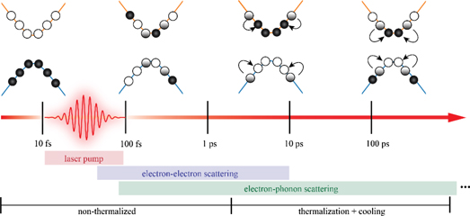
Figure 2. Schematics of electron–electron and electron–ion scattering after laser excitation during a transition to a thermalized regime, and their respective approximate time scales.
Download figure:
Standard image High-resolution imageThe current state-of-the-art approach is the solution of the Kadanoff–Baym equation (KBE) or the Boltzmann (transport) equation, parametrized by static first-principles data. Remarkable agreement with experiments was reported for the thermalization of excited electrons in semiconductors including silicon and gallium nitride; similar theoretical studies also cover metals and noble metals, as discussed in the excellent review in reference [10] and references therein. Explicit first-principles simulations of the real-time electron thermalization dynamics, however, are still much less common and have only been reported for laser-excited nickel, chromium, and copper, using RT-TDDFT [11]. For these systems, in which electron–phonon scattering was excluded, the dynamics is unusually fast. Interestingly, reference [11] points to the need to include the coupling of the electronic system to an external time-dependent potential, such as the ionic system or a laser field, in order to observe electron dynamics in RT-TDDFT with adiabatic exchange and correlation. These findings agree with the picture that electron thermalization involves both electron–electron and electron–phonon scattering [10]. Furthermore, while cooling of thermalized electrons progresses on longer time scales, it also involves electron–electron and electron–phonon scattering as illustrated in figure 2. Even for a given material, it remains a fundamental challenge to understand their relative importance, requiring a simulation framework that treats them on an equal, first-principles footing over long time scales [9, 10]. In order for RT-TDDFT simulations coupled to Ehrenfest dynamics to succeed in this context, the approximate, adiabatic description of the electron–electron exchange–correlation interaction and the mixed quantum–classical electron–ion interaction constitute the biggest deficiencies [11]. Aside from Ehrenfest dynamics, recent developments of surface-hopping techniques can also address the latter problem and have been applied to extended systems [12].
Modelling electron–ion real-time dynamics from first principles would also illuminate the influence of electron–phonon coupling on several carrier–carrier mediated mechanisms. Specific examples that are important in materials after optical pumping include Pauli blocking/state filling and dynamical band-gap renormalization [7], Auger recombination [9], and exciton–exciton annihilation (EEA) [13]. Understanding the time-dependent interplay of Pauli blocking, band-gap renormalization, and excitonic effects is critical to fundamentally understand modern pump-probe experiments [7]. Currently, one of the most accurate models of dynamical band-gap renormalization is based on the time-dependent extension of the Bethe–Salpeter equation (BSE) within many-body perturbation theory, and this was recently applied to monolayer MoS2 [14]. RT-TDDFT was also recently deployed to study band-gap renormalization [7], however, thermalization, i.e. the transition from initially highly excited to thermalized electrons, was not modelled explicitly.
EEA, as an example of exciton dynamics, becomes important in the highly excited regime and in 2D materials. Other radiative and non-radiative exciton recombination channels invoke trions and exciton–phonon coupling [13]. Currently, no explicit real-time first-principles simulations of these processes exist, and the few theoretical interpretations in the literature use predictions from static electronic-structure simulations, based on density functional or many-body perturbation theory. Addressing this critical challenge will allow us to better understand mechanisms that limit their lifetimes and can impact materials selection and design, e.g. to accomplish hot-carrier extraction.
All the mechanisms discussed here are challenges of great interest for experiments and applications, and their time-dependence is currently not well understood. Separating the influence of electronic and lattice contributions to the response, i.e. the screening in a material, is desirable to explain the transition from non-thermalized to thermalized electrons. Doing so entirely from predictive first-principles simulations will allow to analyse (i) the relative importance of electron–electron and electron–phonon scattering, (ii) the dependence on wavelength and intensity of the optical pump, and (iii) the influence of optical transition probabilities in the energy range of interest for a given material.
2.3. Advances in science and technology to meet challenges
Combining RT-TDDFT with Ehrenfest dynamics leads to a simulation framework that enables explicit real-time studies with the exciting prospect of describing both electrons and ions from first principles. However, two main limitations emerge that need to be overcome. First, the adiabatic approximation for the time-dependent exchange–correlation functional is widely, if not exclusively, used. Memory-dependent approximations for the electron–electron interaction could be explored to better understand how this affects dissipation within the electronic system. Recent improvements of the description of the electron–electron interaction within the adiabatic approximation address shortcomings of the local-density or generalized-gradient approximation e.g. by exploring hybrid functionals or the recently developed SCAN meta-GGA approach. Second, approximating the ions as classical particles leads to several well-documented deficiencies of the Ehrenfest dynamics approach. Future advances in the description of electron–ion coupling can, for instance, build on the surface-hopping technique or exploring the exact factorization approach.
That being said, another strong appeal of applying RT-TDDFT to bulk materials is the numerical efficiency; however, the improvements of the method discussed in the previous paragraph will certainly negatively impact this. In order to account for the necessary multi-length and time-scale aspects, computational cost needs to be kept at an absolute minimum.
2.4. Concluding remarks
There is extreme potential for and tremendous interest in a first-principles approach that accurately predicts real-time electron–ion quantum dynamics. Many successful applications of many-body perturbation theory and real-time TDDFT find excellent agreement with experiment and recent progress for both techniques expand the application space. However, this has also exposed deficiencies in the currently used approximations: the next big challenges to overcome lie in the adiabatic approximation of the exchange–correlation functional and the asymmetric quantum–classical description of electronic and ionic system. Addressing these in a computationally highly efficient way has great promise and will certainly advance the field of computational materials modelling and design in interesting directions, with great societal benefit.
Acknowledgments
We gratefully acknowledge financial support from the Office of Naval Research (Grant No. N00014-18-1-2605).
3. Time-dependent density functional theory of ultrafast electron-nuclear dynamics in crystals
Sheng Meng
Institute of Physics, Chinese Academy of Sciences, People's Republic of China
3.1. Status
The ultrafast dynamics of laser-driven electrons and nuclei in crystalline materials, occurring at a time scale ranging from a few attoseconds to hundred femtoseconds, encodes rich information about intense laser–solid interactions [15]. Comparing to isolated molecules in gas phase, the interactions between the laser field and solids are much more complicated, due to the diverse and complex electronic structure of solids and the paramount number of degrees of freedom involved [16]. This calls for an accurate, fully ab initio, state-of-the-art theoretical description of the attosecond dynamics of electrons and nuclei in materials under a strong laser field, going beyond the usual empirical semiconductor Schrödinger/Bloch equations and the adiabatic Born–Oppenheimer approximation.
The advantages of employing a real-time TDDFT approach (figure 3) enable us to simulate correlated quantum movement of electrons and nuclei, the non-equilibrium 'hidden states' [15], as well as exotic couplings between a variety of different degrees of freedom (e.g. lattice and charge) in materials under strong laser fields beyond the perturbative regime [15, 16]. In recent years the field of real-time TDDFT simulations of ultrafast electron-nuclear dynamics has witnessed an explosive growth, with intense efforts devoted into developing faster and more efficient algorithms, accurate simulation of the microscopic optoelectronic processes in realistic materials, and benchmarking theoretical descriptions and predictions against experimental data, together with significant challenges nonetheless being present in the current research frontier and rich opportunities to make further advances. All these advances promise a bright future for real-time TDDFT simulations of electrons and nuclei in laser-driven crystals in the next few years to come.
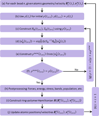
Figure 3. Scheme for typical TDDFT simulations of electron-nuclear dynamics in crystalline materials. Here ρ, Hk
, Sk
,  are the total density of electrons, electronic Hamiltonian matrix, the overlap matrix, and the periodic part of Bloch wavefunctions of the lth-band at wavevector
k
, respectively. This scheme has been combined with ring polymer dynamics for treating quantum nuclear effects. In regular simulations, one usually adopt a classical simulation of nuclei dynamics, namely, n = 1.
are the total density of electrons, electronic Hamiltonian matrix, the overlap matrix, and the periodic part of Bloch wavefunctions of the lth-band at wavevector
k
, respectively. This scheme has been combined with ring polymer dynamics for treating quantum nuclear effects. In regular simulations, one usually adopt a classical simulation of nuclei dynamics, namely, n = 1.
Download figure:
Standard image High-resolution image3.2. Current and future challenges
The past decades have witnessed the great successes of ground-state DFT in capturing static electronic properties of various materials, as exemplified by the Nobel Prize in Chemistry awarded to Walter Kohn in 1998. However, for time-dependent processes, in particular those involving excited states, real-time TDDFT and advanced nonadiabatic algorithms are essential, especially for practical simulations of extended crystalline materials [16–20].
Currently, at the research frontiers of the TDDFT simulation of crystalline materials, various challenges are present that significantly hinder rapid progress in uncovering and understanding the ultrafast dynamics of electrons and atoms in crystals under strong laser fields from a theoretical perspective.
A first and long-lasting challenge is of course the unprecedented computational costs for solving time-dependent Schrödinger equations with quantum many-body effects at an attosecond precision [21]. Since the electronic couplings in crystalline materials usually occur with a strength of a few to hundreds of electron-volts, the corresponding timescale for integrating the electronic equation of motion is sub-attosecond. A tiny period of dynamics running for a few femtoseconds would require millions of molecular dynamics steps at the level of regular DFT calculations, which make the simulation of time-dependent processes prohibitive. The time scale as well as the length scale under simulation (e.g. a real-time simulation of non-equilibrium phonon dynamics would require tens of primitive unit cells) need to be significantly extended to hundreds of picoseconds and supercells comprising thousands of atoms.
Developing new exchange–correlation functionals beyond the adiabatic approximation that can describe the memory effects and excitonic effects are strongly desirable [17]. Since TDDFT is a dynamic theory of matter, knowledge of the history of the electron-nuclear trajectory subject to causality is essential. However, acceptable functionals that capture frequency dependence and such memory effects do not yet exist. Up to today most of the great many TDDFT simulations rely on the adiabatic functionals (such as adiabatic local density approximation) in real applications [16–21]. This raises questions on the validity of calculation of key dynamic properties, such as photocurrents or demagnetization in crystals. Functionals accounting for strong correlation effects, such as the onsite Coulombic Hubbard interactions, are also desirable.
Schemes for calculating time-dependent properties and numerical analysis on the rich information of excited states, particularly for periodic systems, are largely absent. Compared to ground-state DFT calculations, the properties accessible in typical first-principles TDDFT models are scarce and under-developed. The foundation for calculating physical properties in a non-equilibrium dynamic system is under debate, adding to the difficulty in developing efficient schemes to compute such quantities, for example, mechanical modulus, electron and magnetic susceptibility, transient optical absorption, not to mention transient electron–phonon coupling strength, magnetic anisotropy, and topological edge states etc.
A variety of degrees of freedom, such as lattice, charge, spin, orbital, valley, pseudospin, etc, are required to be included in advanced TDDFT simulations of quantum materials. Applications to new forms of materials other than regular metals and semiconductors, e.g. magnetic solids, low-dimensional crystals, materials with nontrivial topology, and superconductors, are still challenging. Applications to new phenomena such as light-enhanced superconductivity and laser-induced quantum Hall effect are yet limited; a strong predictive power from the current TDDFT simulation schemes is expected but seldom demonstrated.
Since the timescale is ultrashort, quantum nuclear effects including zero-point energy and nuclei tunnelling become important and need to be taken in considerations [22, 23]. A majority of TDDFT simulations of crystals performed today only focus on the dynamics of electrons, usually with clamped nuclear dynamics, based on the fact that the mass of electrons and nuclei differs by at least three orders of magnitude. This constraint however can be broken in photoexcited states, since now nuclei may stay on highly unstable high-energy potential energy surfaces, thus the velocity of atoms might approach those of electrons [24]. A small percentage of simulations allow the atoms to move according to the quantum forces acting on them, albeit within a classical approximation of nuclear degrees of freedom, namely all nuclei are treated as point particles. The quantum aspects, such as the zero-point vibration of atoms, splitting of nuclear wavepackets, and quantum tunnelling, which are especially prevalent at low temperatures and for light elements (such as hydrogen, carbon, oxygen), are completely ignored.
3.3. Advances in science and technology to meet challenges
New schemes aimed at performing accurate simulations on the interactions between laser fields and solid-state materials are under intense development. In most previous works, numerical implementations of real-time TDDFT for solids were built upon real-space grids, including some well-known programme packages such as OCTOPUS [18] and SALMON [20]. Real-time TDDFT has also been implemented in plane wave codes, for example, the ELK, FP-LAPW, and FPSID, where encouraging results are obtained to demonstrate the effectiveness of TDDFT approaches [16]. If one is interested in high energy excitations on the energy scale of tens to hundreds of electronvolts, extremely dense real-space grids and high kinetic energy of plane waves are indispensable. By employing a local basis representation built upon numerical atomic orbitals instead [21], propagation of systems of a large size (∼500 atoms) for a long simulation time (∼1000 fs), with a moderate computational cost while maintaining a relatively high accuracy, can be routinely achieved (figure 4). Non-perturbative phenomena in crystalline materials under a strong laser field, as well as linear responses to a weaker field, can be simulated on an equal footing, either in the presence or absence of nuclear movements.

Figure 4. Ultrafast electron dynamics in graphene upon photoexcitation in different laser fields, reproduced from reference [16]. Red and blue dots represent excited electrons and hole respectively. Dot sizes are scaled to the number of photocarriers at each k point.
Download figure:
Standard image High-resolution imageThe electron–hole exchange effect can be adequately described with the new development of the kernels based on BSE and bootstrap functionals [17]. In such approaches to go beyond a single-particle picture, many-body interactions between quasiparticles on the electron–hole basis are explicitly taken into account. At present there is a need to transfer such functionals from the linear response framework into non-perturbative real time schemes. On-site Coulomb interactions can be parameterized based on time-dependent electron densities obtained from first-principles simulations [19].
The combination of length-gauge and velocity-gauge description of external electromagnetic fields has extended the diversity of materials under consideration, ranging from low dimensional systems to periodic solids in laser fields. Meanwhile, by employing a fast propagation algorithm in the reciprocal space, one can simulate real time propagation of thousands of electrons lasting for a few picoseconds with periodic boundary conditions [21]. Exotic phenomena such as nonlinear optical absorption, high harmonic emission, high-order resonant energy transfer, and electron–phonon coupling in excited states can be described accurately in such a scheme [24–28].
To consider nuclear quantum effects in ultrafast processes, a practical computational scheme combining real-time TDDFT and so-called ring polymer molecular dynamics (RPMD) based on imaginary-time path integral simulations of nuclear trajectory has been recently introduced [22]. This approach allows us to treat quantum nuclear effects in nonadiabatic excited state dynamics involving many potential energy surfaces. Generalizing exact path integral molecular dynamics for static equilibrium properties, RPMD is a simple approximate technique to describe real time quantum dynamics, which has been used to calculate chemical reaction rates and the quantum diffusion in liquid water in the ground state [23]. The RPMD approach provides quantum statistics and semi-classical dynamic descriptions by constructing a fictitious polymer for the original system. This polymer is comprised of N replicas (beads) of the real poly-atom system and each bead of the same atom is linked by harmonic spring interactions. According to the isomorphism between a quantum particle and classical ring polymer, the bead configuration in real-time trajectory can be regarded as the possible existing state of a quantum particle. In such quantum electronic-nuclear dynamics simulations, real-time TDDFT calculations provide the information of ionic forces, electronic energy and stress tensor, while RPMD deals with the evolution of atomic positions and velocities (figure 3). This method can go beyond the mean-field Ehrenfest approach in the sense that correlations between electrons and nuclei are recovered by propagating electronic wavefunctions for each bead of the ring polymer [22]. Potential areas for applications of such a full quantum approach include calculating the broadening and redshift of optical absorption spectral peaks in diamond nanocrystals due to quantum nuclear effects [29], developing strategies for optical manipulation of quantum paraelectrics such as SrTiO3 [30] and atomic tunnelling rates in BaTiS3 [31].
3.4. Concluding remarks
The new developments and applications of real-time TDDFT simulations of ultrafast dynamic processes in crystalline materials represent a significant step towards a full quantum description of electronic and nuclear states from first-principles. This approach has the potential to provide a comprehensive and predictive understanding of quantum interactions and dynamics of complex materials at the atomic and attosecond scale. These advances open new opportunities for studying, and ultimately, controlling, the ultrafast quantum dynamics of a variety of quasiparticles and a broad range of nonlinear strong-field behaviour in crystals.
Acknowledgments
We acknowledge financial support from NSFC (Grant Nos. 91850120, 11934003, and 12025407), MOST (Grant No. 2016YFA0300902), and 'Strategic Priority Research Programme B' of the CAS (No. XDB330301).
4. Ultrafast materials design with classical and quantum light
Michael A Sentef1, Michael Ruggenthaler1 and Angel Rubio1,2,3
1Centre for Free Electron Laser Science (CFEL), Germany
2Universidad del País Vasco UPV/EHU, Spain
3The Flatiron Institute, United States of America
4.1. Status
Ultrafast pump-probe spectroscopy has allowed researchers to disentangle the microscopic degrees of freedom of materials (charge, spin, orbital, lattice). Moreover, by employing the energy–time complementarity, low-energy collective excitations, whose frequency-domain signatures require high resolution, are more easily probed in the time domain, where their coherent oscillations are slow. More recently, the focus in the field has shifted away from interrogating quasi-equilibrium properties towards the creation of new light-induced states of matter without any equilibrium counterparts. In the following we discuss selected examples of light-induced states, both for the case of strong laser driving ('classical light') and for matter in dark cavities ('quantum light').
One of the highlights of this extremely active field of research was the demonstration of possible light-induced superconductivity [32]. Upon driving the crystal lattice with mid-infrared light pulses the low-energy optical conductivity of K3C60 was shown to exhibit superconducting features even far above its equilibrium superconducting critical temperature. Similarly, spectacular results have by now been demonstrated in a variety of different superconductors, among them several classes of cuprates as well as an organic kappa salt compound [33].
A related class of light–matter coupled phenomena coined Floquet materials engineering was also recently demonstrated in solids. Here the key idea lies in the fact that periodically driven systems can be mapped stroboscopically onto quasi-static ones through the Floquet theorem. This has been employed in nearby research fields, for instance in atomic and molecular physics as well as quantum simulators with cold atoms or trapped ions. In solids a breakthrough was achieved by observing Floquet–Bloch states on the surface of a topological insulator using time-resolved photoemission spectroscopy [34] (see figure 5). Another more recent highlight was the report of the light-induced anomalous Hall effect [35] motivated by earlier theoretical predictions.

Figure 5. Floquet–Bloch states observed on the Dirac-fermion surface state of a three-dimensional topological insulator, Bi2Se3 [33]. Reproduced with permission from Fahad Mahmood.
Download figure:
Standard image High-resolution imageA complementary development in the research of novel light–matter coupled states was achieved in the field of polaritonic chemistry. This field has been stimulated by ideas from cavity quantum electrodynamics (QED) to manipulate matter with pure vacuum fluctuations of quantum light. The design of properties on demand in quantum materials by placing them in controlled QED environments (quantum cavities) was inspired, for instance, by the observation of enhanced ultrafast non-radiative energy transfer between cyanine dyes in a cavity [36]. This significant change is due to the emergence of hybrid light–matter states called polaritons, whose ultrafast dynamics can be revealed by pump-probe experiments [37]. The theoretical description of these novel states of matter requires a quantum treatment of the light field and has some resemblance to the Floquet approach for classical light [38]. This suggests that ideas for engineering material properties by periodic driving can be readily transferred to the cavity QED situation. The emergence of polaritons and changes in material properties is quite universal and is not restricted to only molecular systems. For instance, in the case of a 2D electron gas, strong light–matter coupling can lead to large modifications of the magneto-transport properties [39].
The field of cavity engineered quantum materials and their emergent electronic properties is still in its relative infancy. Before discussing its intriguing opportunities and key challenges below, let us highlight a few recent developments that showcase its enormous potential. In close similarity to ideas based on Floquet engineering to control the superconducting behaviour of materials by periodic driving, it was theoretically predicted that the electron–phonon interaction in a monolayer of FeSe on the dielectric substrate SrTiO3 is enhanced through the formation of phonon polaritons at the FeSe/SrTiO3 interface when the system is placed inside a QED cavity (see figure 6). This cavity-controlled electron–phonon coupling was predicted to systematically affect superconductivity in that material [40] and in many others.

Figure 6. Illustration of predicted cavity-controlled electron–phonon coupling and superconductivity in monolayer FeSe on SrTiO3 substrate [39]. Reproduced with permission from Joerg M. Harms, MPSD.
Download figure:
Standard image High-resolution imageA closely related experiment was indeed reported with similarly striking results. Researchers employed the strong near-field SPPs on a gold surface coupled to phonon modes of a polymer matrix, to modify the superconducting critical temperature (TC) in two very different superconductors, Rb3C60 and optimally doped YBCO [41]. Magnetometry measurements showed that one of the fingerprints of superconductivity—the Meissner effect—could be induced at significantly different TC compared to the samples without the QED environment. Indeed, an enhancement of TC from 30 to 45 K was found for Rb3C60, whereas a suppression from 92 to 86 K was reported for YBCO.
4.2. Current and future challenges, and advances needed
Here we categorize key challenges that in our view require dedicated attention, namely the control of detrimental effects (strong lasers, heating, short lifetimes) in classically-driven materials, the achievement of strong light–matter coupling under controlled materials conditions in different QED settings, as well as the development of theoretical and computational approaches enabling the description and prediction of ultrafast time-domain phenomena in available or designed quantum materials.
- (a)Classical light: control of heating, extension of lifetimes of novel states of matter, selective ultrafast switching. Despite the promises to create properties on demand with controlled laser pulses and no shortage of creative theoretical proposals, clear-cut demonstrations of Floquet states in solids have still been scarce to this date. Three of the key issues are: (i) the need for strong laser pulses, (ii) the accompanying heating of the sample, and (iii) the limited lifetime of the induced states. It is important to further develop experimental techniques that push the boundaries in this respect. For instance, the use of tailored laser excitations in the mid-infrared [32], which in certain situations and in particular anisotropic geometries can avoid electronic heating, has been an important step forward. Another big step lies in the identification of scenarios in which driving with selective light pulses allows for ultrafast optical control of a collective condensate with promising functionalities (cf section by Radu). As an example, the switching of chiral condensates with emergent Majorana edge modes by circularly polarized light has been suggested [42], which might eventually find an intriguing application in the optical programing of Majorana-based quantum logic gates. However, there are various challenges to overcome before this becomes a reality. Besides the need for the synthesis and clear-cut identification of a chiral topological superconductor as a materials platform, also the development of tailored laser pulses (pulse shaping) that can be applied at sufficiently low temperatures, as well as corresponding probing techniques (cf section by Murnane, Shi and Kapteyn), remain a major challenge that researchers in the field should tackle within the next decade.
- (b)Quantum light with strong coupling: new device fabrication and probing schemes. The cavity approach has several appealing features, compared to classical light: (i) strong external fields are not necessary; (ii) there is thus much less heating of the sample; (iii) hybrid light–matter states can have very long lifetimes; and (iv) quantum aspects of light can be important also on very short subcycle time scales. Indeed strong-light matter coupling appears to be robust and can be achieved even at ambient conditions. However, the main challenge is to reach strong light–matter coupling in the first place. Depending on the situation there are several standard ways to do so: (a) to increase the collective coupling to the QED environment by increasing the matter density, (b) to increase the quality factor of the cavity, or (c) to minimize the mode volume of the cavity. To gain a detailed microscopic understanding of the strong-coupling process ultrafast experiments investigate subcycle switch-on of strong coupling [43]. The emerging subcycle QED allows for applications such as the measurement of vacuum fluctuations of the light field [44]. Another important research direction is the use of an auxiliary material that couples itself strongly to the light field and mediates the strong coupling to the sample of interest [40]. Here it would be desirable to achieve similarly strong couplings in well-defined atomically controlled heterostructures. Moreover, the crossover between the quantum regime of cavity QED and the ultrafast classical regime, specifically with respect to the modification of materials properties, is largely unexplored and provides ample opportunity for future experimental and theoretical research [45, 46]. First results indicate that the concept of Floquet engineering of microscopic materials parameters can be implemented both in the classical-light regime (weak light–matter coupling, many photons in a coherent state) or in the quantum-light regime (strong light–matter coupling, few photons in a Fock state, i.e., with zero macroscopic electromagnetic field) [45].
- (c)Development of comprehensive theoretical frameworks able to describe ultrafast phenomena and predict properties of nonequilibrium and cavity materials. On the theory side many aspects of ultrafast dynamics and cavity-controlled modifications of material properties remain challenging. So far, the standard approach is to extend quantum-optical or solid-state models to light–matter coupled systems in order to rationalize experimental findings. But such an approach clearly needs insights about which degrees of freedom are important. A detailed understanding of many of the observed effects, however, is currently missing, which limits the predictive power of such models. Therefore, an unbiased approach that treats all microscopic degrees of freedom on an equal footing is desirable. However, in that case first-principles approaches need to solve a quantum-field theoretical QED problem, which is of course even much harder than the many-body Schrödinger equation on its own. The newly developed quantum electrodynamical density functional framework is one of the promising approaches to achieve this goal [47], and first-principles simulations of QED–matter systems were recently reported [48]. A particularly appealing feature of this framework is that it reduces for zero coupling to the photon field to (TD)DFT. Therefore, it can be nicely combined with advanced methods of TDDFT as discussed by Dos Santos and Schleife or also Meng in this roadmap.
4.3. Concluding remarks
We are only at the beginning of a systematic exploration of novel phenomena enabled by light–matter coupled quantum many-body materials and their potential use for future quantum technologies. We believe that the interface between highly active and successful research fields—quantum optics, quantum materials and 2D heterostructures (cf section by Murnane, Shi and Kapteyn or Dani and de Jornada), ultrafast spectroscopies, nanoplasmonics, polaritonic condensates, and polaritonic chemistry—will offer a plethora of unexpected discoveries and an interesting platform to explore new phases of matter [49]. In particular, ultrafast spectroscopy using quantum light is expected to lead to novel insights into the interplay of microscopic degrees of freedom and their ultrafast dynamics upon laser excitation, while the combination of strong light–matter coupling and ultrashort laser pulses opens opportunities for the creation of properties on demand in quantum materials in the time domain.
Acknowledgments
MAS acknowledges financial support by the DFG through the Emmy Noether programme (SE 2558/2-1). AR and MR acknowledge financial support by the European Research Council (ERC-2015-AdG694097), the Cluster of Excellence 'CUI: Advanced Imaging of Matter' of the Deutsche Forschungsgemeinschaft (DFG)—EXC 2056—project ID 390715994 and the SFB925 'light induced dynamics and control of correlated quantum systems'. The Flatiron Institute is a Division of the Simons Foundation.
5. Ultrafast magnetism: experiments
Ilie Radu
Freie Universität Berlin, Germany
Max Born Institute, Germany
5.1. Status
Long-range magnetic ordering arises from the subtle interplay between quantum mechanical effects and relativistic interactions. Therefore, a prerequisite to understand non-equilibrium magnetic phenomena, and a key challenge of the ultrafast magnetism field, is the complete knowledge about the time- and length-scales pertinent to the microscopic interactions governing the magnetic order, e.g. the exchange interaction, spin–orbit coupling, and the magnetic dipole–dipole interaction. As shown in figure 7, these span the timescales from attoseconds (10−18 s) to nanoseconds (10−9 s) and the length scales from angstroms (10−10 m) to micrometers (10−6 m).

Figure 7. The relevant time and length scales for ultrafast magnetic phenomena. Reproduced with permission from [15].
Download figure:
Standard image High-resolution imageBroadly speaking, the field of ultrafast magnetism encompasses the non-equilibrium spin and magnetization phenomena driven by an ultrashort external stimulus. Such a stimulus could be, for instance, an ultrashort pulse of light, a fast charge and/or spin current burst or a pulsed magnetic field [50, 68]. Due to their ability to provide real-time information about, and experimental access to the microscopic processes (e.g. spin–electron–phonon scattering) and magnetic interactions governing non-equilibrium magnetism, the use of femtosecond laser pulses is of particular interest and relevance. Moreover, such intense and ultrashort laser pulses are well suited for manipulation and control of magnetization at unprecedented speeds, ideally on timescales as fast as the driving pulse itself.
Being highly relevant for both fundamental and applied science, the ultrafast magnetism field has undergone an intense activity and development over the past decades, both experimentally and theoretically [68]—see section 6 by P M Oppeneer for a perspective on the theory of ultrafast magnetic spectroscopy. Since the first report of a laser-induced, sub-picosecond demagnetization of ferromagnetic Ni in the seminal work of Beaurepaire, Bigot and collaborators [51], the field has witnessed spectacular demonstrations of how ultrashort bursts of light can affect the magnetic order ranging, for instance, from ultrafast magnetization quenching on a few fs timescale [52] to laser-induced magnetization generation [53] and from coherent spin precession at THz frequencies [54] to all-optical magnetization switching (AOS) [55, 56].
The conventional approach to investigate ultrafast magnetic phenomena was the employment of pump-probe techniques using fs laser pulses in the visible spectral range (400 nm to 800 nm) to photo-excite and subsequently probe the magnetic matter. Magneto-optical (MO) probing techniques (like the Kerr and Faraday effects) have been used to monitor the laser-induced spin dynamics. Although these approaches reveal the first glimpses of ultrafast spin dynamics [50–51, 53, 55, 57], they provide only an indirect measure of magnetization dynamics. This limitation stems from the fact that all-optical pumping and probing beams are non-specific with respect to the constituent magnetic elements, the sample sub-systems (e.g. charge, lattice, spin, and orbital degrees of freedom), and their excitations (e.g. phonons, magnons, electron–hole pairs). It was soon recognized that, for a thorough understanding of ultrafast magnetic phenomena, there is an utmost need for time-resolved spectroscopic techniques providing such element-, sub-system-, and quasiparticles-specificity with fs time resolution and down to atomic scale spatial resolution.
5.2. Current and future challenges
Such capabilities, which brought the ultrafast magnetism field to the next level, have become readily available only in recent years with the advent of novel light sources generating ultrashort and intense THz/mid-IR and x-ray radiation, using either laser-based schemes or synchrotrons and free-electron lasers (FEL). For instance, high-field THz pulses are now almost routinely used to resonantly and selectively excite quasiparticles (phonons [58] and magnons [54, 59]) to drive ultrafast spin dynamics or even to trigger magnetic phase transitions [60]. Also, femtosecond x-ray pulses turned out to be extremely powerful tools to monitor and disentangle the element-specific spin and orbital dynamics of magnetic alloys and heterostructures during, for instance, the laser-driven demagnetization [61] and magnetization switching processes [56], or on extremely fast timescales during the coherent light–matter interaction [52]. X-ray FELs are useful tools in this context since, due their high intensity/brilliance, short pulse structure and wavelength tunability from XUV to hard x-rays, can provide both femtosecond time- and nanometer spatial-resolution, see e.g. reference [62].
All-optical magnetization switching: beside the fundamental scientific interest in exploring and understanding ultrafast magnetism, the field bears an exciting potential for technological applications in high-speed magnetic logic and magnetic storage devices. In this respect, the most appealing phenomenon is the so-called AOS, denoting magnetization reversal driven by a fs laser pulse alone without any external magnetic field [55]. Initially discovered in ferrimagnetic GdFeCo alloys [55, 56] and later shown to occur in various magnetic systems (synthetic ferrimagnets, ferromagnets, iron garnets) [68, 66], AOS represents the fastest magnetization reversal mechanism known so far, with switching times on picosecond timescales. With obvious advantages (i.e. ∼1000-fold faster, no external magnetic field required) when compared to the current magnetic recording techniques, the potential of AOS has been recognized by the computer and data storage industry, which considers the AOS process as an alternative, emerging magnetic recording technology.
A crucial requirement to understand ultrafast magnetism, and particularly AOS, is the ability to obtain real-time and real-space information about the transient evolution of the spin ensemble, from the initial photo-excitation event to the full relaxation of the system. As shown in figure 7, this implies measuring spin dynamics over many orders of magnitudes in time- and length-scales, essentially requiring a multi-scale probing tool. Moreover, as the spin system continuously and mutually interacts with other degrees of freedom [like charge, orbital angular momentum (OAM), lattice], one needs to monitor and disentangle their dynamic behaviour, both in the spatial and temporal domains. Hence, a key challenge is obtaining a complete and simultaneous spatio-temporal measurement of the non-equilibrium spin dynamics, complemented by a full spectroscopic description of the individual dynamics of all constituent degrees of freedom.
Existing ultrafast techniques lack the required combination of time and spatial resolutions; for instance, XUV HHG sources do provide attosecond time resolution (see e.g. reference [52] and section 7) but have poor spatial resolution, whereas XFEL sources can probe the magnetic matter down to ∼10 nm length scales with only tens of fs time resolution. Future advances in XFEL capabilities towards attosecond FELs [64] complemented by progress in table-top light sources and ultrafast instrumentation will provide unprecedented opportunities in measuring and controlling spin dynamics as well as spin-related processes and interactions on their natural time and length scales.
Ultrafast angular momentum flow: another major issue challenging our understanding of ultrafast magnetism is angular momentum conservation and dissipation during an ultrafast, laser-induced change of magnetization [50, 68]. The angular momentum transfer rate is a crucial parameter for any spin dynamics experiment (demagnetization, magnetization reversal, etc) since it will ultimately set the speed and the magnitude change of magnetization. Whereas it is commonly believed that the atomic lattice will eventually act as a final sink of angular momentum, the microscopic pathways of angular momentum exchange among the laser pulse, electronic orbitals, spins, and surrounding lattice are essentially unknown. The angular momentum dissipation and transfer terms are equivalently used here to denote reversible spin dynamics processes responsible for removal of angular momentum out of the spin sub-system.
Recent time-resolved x-ray diffraction studies have suggested [65] that most of the angular momentum dissipated upon ultrafast demagnetization appears within 200 fs as a lattice distortion in the form of a surface acoustic phonon. These findings have been corroborated by femtosecond soft x-ray MCD measurements (able to monitor the spin and orbital moments dynamics), showing that the lattice can accommodate 100% of the angular momentum dissipated within ∼500 fs during the fs laser-induced demagnetization process [61]. Although groundbreaking, these works did not reveal the intermediate steps of angular momentum transfer from the initial photoexcitation to the lattice. Future studies employing lattice-, spin-, and orbital-sensitive probing tools with time resolutions down to 1 fs (in metallic magnets the dynamic orbital momentum quenching by the lattice is expected to occur on ∼1 fs timescale or faster) should be able to reveal the intriguing complexity of the angular momentum dissipation from and into the spin system.
Towards attosecond magnetism: one of the most intriguing yet largely unexplored area of ultrafast magnetism is the coherent light–spin interaction occurring on the timescale of the photo-excitation event itself—see figure 8. Although the first steps have been taken in this direction, in the pioneering work of Bigot et al [57] and more recently by Siegrist et al [52], the field of coherent magnetism is in a very incipient phase. Ultrashort, single-cycle laser pulses (at wavelengths from the THz to the visible) offer intriguing possibilities with respect to coherent magnetization effects: given that the spin system can follow the field (either E or B field component) of the exciting pulse in a phase-locked manner (cf figure 8) one could excite spin dynamics on timescales substantially faster than a single oscillation cycle of the driving pulse, i.e. well into the attosecond regime.

Figure 8. Pictorial view of the coherent interaction between spins and a single-cycle laser pulse (red solid line). The strong electric E field of the laser could modulate the exchange interaction and affect the spins orientation and magnitude via an E field-orbit–spin interaction or alternatively the laser pulse could couple to the spins via Zeeman interaction with the magnetic B field; such a coherent light–magnetic matter interactions should provide the ultimate time scales for spin manipulation with light.
Download figure:
Standard image High-resolution imageWe envisage future studies addressing such coherent magnetization processes and their effects on the average magnetization of spin ensembles in various functional magnetic materials. Such an experimental approach in combination with an element-specific probing of spins [52, 56] will reveal the genuine microscopic processes and interactions involved in photo-driven coherent magnetic phenomena, and thus bridging critical gaps in our understanding of ultrafast magnetism.
5.3. Concluding remarks
Looking back, the ultrafast magnetism field has come a long way from the first report on sub-ps demagnetization of nickel in 1996 [51] to the first attosecond MCD measurements reported recently [52]. New and sometimes unexpected magnetic phenomena driven by ultrashort laser pulses have been discovered [50, 51–66, 68], like the pure optical control of magnetism [55] or the generation of transient magnetic states with no counterparts in the equilibrium phase diagram of the investigated magnets [56], to name just a few. To a large extent, the key enablers of such breakthrough studies were the fast-developing technological and instrumental advances in ultrafast science. Covering essentially the entire spectral range from THz to hard x-rays, both at a table-top and large-scale facility level, such an 'ultrafast science toolbox' has played a pivotal role in our understanding of the ultrafast light–magnetic matter interaction.
Looking ahead, the 'ultrafast toolbox' will continue to expand by adding new capabilities (e.g. attosecond light pulses, ultrafast electron bunches, ultrashort and ultrastrong electric and magnetic fields, phase-locked THz and x-ray pulses) with the aim of obtaining real‐time and real-space observations of electron, lattice, and spin motion, essentially with attosecond time resolution and down to atomic length scales. New electronic and magnetic phenomena are to be revealed, occurring especially in the 'terra incognita' of ultrafast magnetism, i.e. during the first 10 fs after laser excitation and faster. On a more applied level, novel material-based approaches and different magnetic material classes will be investigated [66–68] targeting low-energy-dissipation and deterministic control of magnetic order parameter on ultimately fast time and length scales.
Acknowledgments
Funding from the German Federal Ministry of Education and Research (BMBF) through project 05K16BCA (Femto-THz-X), from the German Research Foundation (DFG) through TRR227 (ultrafast spin dynamics) and from European Research Council through TERAMAG (Grant No. 681917) is gratefully acknowledged.
6. Ultrafast magnetic spectroscopy—theory
Peter M Oppeneer
Uppsala University, Sweden
6.1. Status
The spectroscopy of magnetic materials has a long history, starting with the initial discoveries of the Faraday and MO Kerr effects in the 19th century. Over the years the sensitivity of magnetic spectroscopies has been tremendously improved, to the extent that it is nowadays feasible to detect, in a nondestructive way, the tiniest magnetic response e.g. from a magnetic molecule on a surface or a magnetic impurity in a crystal. A further dimension was added to magnetic spectroscopy two decades ago: pulsed light sources that could deliver femtosecond laser pulses became available and made it possible to perform magnetic spectroscopy in the fs-time domain using the pump-probe technique. Employing this technique, Beaurepaire et al discovered ultrafast laser-induced demagnetization [51] which led to the birth of a whole new research area: that of ultrafast magnetism, or femto-magnetism.
This first ultrafast demagnetization experiment revealed an extremely fast quenching of the magnetization in some 250 fs, pointing to a previously unthought-of fast interaction of spins and photons [51]. The discovery has far reaching consequences for the speed with which spins can be manipulated with electromagnetic fields—it could be orders of magnitude faster than expected previously. Moreover, the discovery lay bare that the fundamental interaction of magnetism and light at ultrashort timescales was only poorly understood. Knowing how to manipulate spins with light pulses at the fs timescale could establish new pathways to construct ultrafast spintronic or opto-magnetic devices. Since then, both the origin of ultrafast magnetization dispersal and the interpretation of the measured MO response have been intensively debated [68] (see also section 5 by I Radu). A recurrent question has been: where does the spin angular momentum go on fs-timescales? This relates to the on-going discussion on the mechanisms of ultrafast demagnetization, and how advances in theory for ultrafast magnetism and spectroscopy can contribute to solve this issue. Another recurring question focuses on the interpretation of the response measured with pump-probe magnetic spectroscopy: what is precisely measured with this spectroscopy?
6.2. Current and future challenges
In static equilibrium, MO spectroscopy relates directly to the magnitude of the sample magnetization. To extract the purely magnetic signal requires a magnetization-related change of the MO spectrum yet without it being affected by 'dichroic bleaching', i.e., a change caused by the optical charge response [68, 69]. Disentangling charge and spin responses is a current challenge which plays a key role in drawing conclusions on mechanisms of ultrafast demagnetization.
Considering, for example, the x-ray magnetic circular dichroism (XMCD) effect, a purely magnetic signal would require a similar, magnetization-related change in the absorption coefficients  , for right and left circularly polarized light, with
  , the transient magnetization, but without a change of
  . In the context of ultrafast demagnetization
  and
and  were only recently studied carefully. Figure 9(a) shows the first measurements of μ+, μ− performed at the Pt L3 edge of ferromagnetic FePt using an x-ray free electron laser [70]. The measurements show the expected 'magnetic' behaviour, i.e., mirror symmetry around the μ = 1 axis, implying that a magnetic signal proportional to the Pt 5d magnetic moment was obtained. For comparison, in figure 9(b) the transient absorptions (TA) measured in the first 150 fs at the Pt N7 edge of ferromagnetic CoPt are shown [71]. In this case, μ+ and μ− do not show a mirror-type behaviour, which implies the presence of a sizeable charge, not magnetic, contribution to the magnetic spectrum. The CoPt measurements further showed a similarly fast magnetization decay (∼90 fs) of the atomic moments on Co and Pt, whereas the FePt measurements observed a fast demagnetization on Fe but a much slower one on Pt (∼600 fs) [70], despite the similar electronic structures of these materials. These rather disparate observations led to different mechanisms discussed for ultrafast demagnetization in FePt (fs-magnon generation) and CoPt (optical inter-site spin transfer, OISTR [72]), which emphasizes that a comprehensive understanding of the fs MO signal is essential for drawing conclusions on the demagnetization mechanism.
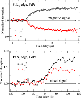
Figure 9. Comparison of pump-probe XMCD measurements of the time-resolved Pt magnetic moment in FePt (top) (reproduced from [70]. CC BY 3.0.) and CoPt (bottom) (reproduced from [71]. CC BY 4.0.). The mirror symmetry around the μ = 1 axis in the μ+ and μ− absorption coefficients at the Pt L3 edge (top panel) represents a purely magnetic signal, attributed to ultrafast magnon generation [70]. The absence of mirror symmetry in the XMCD measurements at the Pt N7 edge (bottom) signifies a significant charge response at noticeably short times, attributed to optical inter-site spin transfer from Pt to Co [71]. Note the different scales of the axes.
Download figure:
Standard image High-resolution imageComing back to the origin of ultrafast demagnetization, several mechanisms have been proposed to explain the ultrafast removal of spin angular momentum (see [68]), such as transfer of spin angular momentum to phonons, photons or magnons, through local spin–flip interactions, or alternatively, nonlocal spin transfer, such as superdiffusive transport [73] or OISTR [72]. A current challenge in magnetic spectroscopy is to provide conclusive evidence for a specific mechanism. This task is nontrivial; for example, both superdiffusion [73] and OISTR [71] transfer spin in the sample, with a distinction that OISTR takes place during the optical excitation.
Understanding these processes becomes even more important for the technological relevant all-optical magnetization reversal driven by short laser pulses [74]. Here, one of the discussed mechanisms is a nonlinear MO effect, the inverse Faraday effect (IFE), in which an intense laser pulse induces a local static magnetization,  where Mind is the coherent induced magnetization that is present during the pump and then decays [75]. In spite of its relevance, an unambiguous identification of this effect still needs to be made. On a more general note, the use of highly intense pump pulses in fs magnetic spectroscopy brings with it that non-linear contributions (∼E2) become significant. These add an additional static magnetic contribution Mind to the demagnetization signal that needs to be distinguished from linear MO and nonmagnetic electronic contributions.
6.3. Advances in science and technology to meet challenges
Scientific advances are needed to correlate better magnetic and electronic structure modifications due to intense pump pulses and be able to disentangle them. One approach that was recently used, is to employ two complementary ultrafast spectroscopies on the same sample in one setup, e.g. time-resolved MOKE and angular resolved photoemission spectroscopy (ARPES) (see section 7 by M Murnane et al), which gave a consistent magnetization decay time (∼170 fs) for Ni [76] even though the pump pulse did modify the electronic structure. The differences in the transient XMCD spectra of CoPt and FePt (figure 9) underline that systematic measurements at various core edges must be performed and correlated with ab initio calculations for their MO responses to understand if, and why, different core and semi-core levels could yield contrasting conclusions.
A clearer identification of ultrafast demagnetization channels needs to be achieved, in a material-specific way. Although it is evident that hot electrons transfer their energy to cold phonons [51], a rigorous observation of spin angular momentum transfer to phonons still needs to be made; a first step in this direction was made recently [65]. Demagnetization due to angular momentum transfer to magnons was observed [77] and also due to superdiffusive spin transfer [78], but these too, need further examination. For example, which phonon or magnon modes are at play in the dynamics? Also, theory treating explicitly electron–magnon/phonon scattering is requested on several levels, including semiclassical Boltzmann theory and time-dependent many-body theory [79].
Understanding the situation during pump-probe overlap and immediately after the pump pulse is a complicated task. Dichroic bleaching causes a modification of the XMCD signal [68] looking similar to the effect of OISTR [71]. How can the effect of an on-site electron excitation be distinguished from that of an optical inter-site transition? In a picture of electron wavefunctions extending over several atomic sites it might not be possible to trace this experimentally and advances in theory will be needed to pinpoint essential distinctions.
On the theory side, TDDFT is well suited to describe the time-evolution of the single-particle wavefunctions in an external field [80]. As was pointed out early on, to treat the demagnetization adequately the energy flow from the hot electrons to the phonons and magnons must be considered [51, 81]. However, currently in most TDDFT calculations the pump energy stays in the electron system, which restricts its applicability range to ∼100 fs or less, i.e. before energy transfer to phonons/magnons occurs. Recently, transfer of spin to OAM has been studied within TDDFT [82]. Further inclusion of energy transfer to phonons/magnons will be needed to treat longer timescales (for recent progress in this direction, see section 3 by S Meng).
6.4. Concluding remarks
Ultrafast magnetic processes measured with pump-probe spectroscopy happen under non-equilibrium conditions and involve coupled spin, charge, orbital and nuclear degrees of freedom. Current theoretical approaches cannot capture their time-evolution without making restrictive approximations. Consequently, although ultrafast magnetic spectroscopy has been employed over the past twenty years, its full bearing on explaining ultrafast magnetism has not been achieved yet. There is much room for development of both theoretical and experimental advances, in particular to unambiguously match measured time-resolved magnetic spectra with theoretical spectra to be able to conclusively identify the origin of the underlying ultrafast magnetic processes.
Acknowledgments
PMO acknowledges financially support by the Swedish Research Council (VR), the German Research Foundation (DFG) through TRR227 (ultrafast spin dynamics), the European Union's Horizon 2020 programme (Grant No. 737709, FEMTOTERABYTE) and the K and A Wallenberg Foundation (Grant No. 2015.0060).
7. Probing and manipulating magnetic and 2D quantum materials using ultrafast laser and high harmonic sources
Margaret M Murnane, Xun Shi and Henry C Kapteyn
University of Colorado and NIST, United States of America
7.1. Status
The ability to probe the full dynamic response of quantum materials on the length- and time-scales (Å and attoseconds and up) fundamental to charge, spin and phonon interactions is leading to a host of new discoveries. The coupled interactions between charges, spins, orbital, and lattice degrees of freedom are key to determining the state of a material, whether metallic, insulating, superconducting, or magnetic. Under thermal equilibrium conditions these states can be tuned by varying the temperature, pressure, chemical doping, or dimensionality. However, their inherent complexity and rich phase landscape make them challenging to understand or manipulate deterministically. Fortunately, ultrafast light sources have undergone remarkable advances in recent years, achieving what was merely a dream three decades ago, i.e., full coherent control of light fields spanning the THz to the x-ray regions. These new capabilities are providing powerful new tools for coherently manipulating and probing quantum materials using light.
7.2. Current and future challenges
Recent advances in HHG have provided new techniques for uncovering new phases and couplings in 2D and magnetic materials. A femtosecond laser can coherently manipulate and tune the properties and interactions in the material, while HHG is a powerful probe to map these new phases and couplings [83–86, 104]. There are several beautiful recent observations of exciting new states in materials using light—however, in some cases, the limited experimental data points made it challenging to validate an interpretation. The new ability of ultrafast HHG-based photoemission [83–86, 98, 99, 102] and magneto-optic spectroscopies [86, 95, 103] to precisely probe multiple phases, electronic and magnetic order parameters, when combined with scanning the laser excitation fluence, is allowing us to map how material phases, magnetic states, and electron–phonon–spin couplings interplay in these delicate materials [87]. One aspect that facilitates the precise manipulation of materials using light is the large separation in timescales between the charge, spin, and phonon dynamics. Much effort has been devoted to coherent control of molecular systems, and the prospects for similar control in quantum materials systems are just as exciting and appear even more achievable.
7.3. Advances in science and technology to meet challenges
High harmonic generation: the HHG process has made it possible to generate bright attosecond-to-femtosecond pulse trains or pulses, that can capture the fastest coupled charge, spin, phonon, and transport dynamics in materials and nano systems. Recent advances in HHG have made it possible to extend bright HHG from the EUV region into the vacuum ultraviolet (VUV) and soft x-ray regions, with spectral, temporal, and polarization properties that are ideal for a host of ultrafast spectroscopies [88, 89]. It is now possible to generate bright HHG into the soft x-ray region of the spectrum at >kHz repetition rates required for advanced spectroscopies. It is also possible to create polarization and phase structured HHG beams (spin and OAM) to enhance contrast, and to implement unique excitations and probes of chiral structures in magnetic materials and nanostructures [90–92]. There have also been significant advances in generating light in the VUV spectral region (∼6–18 eV), a spectral region uniquely suited to probe chemical processes, as well as time- and spin-resolved angle-resolved photoemission spectroscopy (trARPES—see section 8 by Stadtmüller). It harnesses a new highly cascaded harmonic generation process where UV and VUV spectral lines are produced through upconversion of an infrared fibre laser such that each harmonic contributes to the cascaded formation of higher harmonics. A significant advantage of this process is that the peak intensity required for this process is in the range of 1012 W cm−2—substantially lower (×10–100) than that required for HHG, correspondingly lowering the pulse energy needed for VUV generation. This makes it possible to produce high flux, high repetition rate (100 kHz to >MHz) pulses in a photon energy range from the UV to 18 eV, with variable energy (∼10–40 meV) and time resolution (∼50–100 fs) [88]. Cavity-based HHG was also demonstrated to achieve a repetition rate of tens of MHz [100, 101]. These new HHG capabilities, that span the VUV, EUV, and keV regions, are ideal for a suite of ultrafast x-ray absorption spectroscopies, photoelectron spectroscopies, and magneto-optic spectroscopies.
Ultrafast electron calorimetry: key to using the capabilities of these new light sources to understand quantum materials is a new approach we call ultrafast electron calorimetry [83–86]. Using HHG-based trARPES, we can measure the full dynamic electronic band structure and electron temperature. Since the electrons thermalize very quickly and their heat capacity is small, heat transfer from the electrons is directly monitored. By varying the laser excitation fluence while monitoring this electron temperature at very short times, we can sensitively detect the changes in the microscopic interactions. When coupled with the ability of HHG trARPES to simultaneously capture the full dynamic band structure (which reflects the macroscopic order parameter), we can map and expand the phase diagram using light as a tuning parameter. In recent research, we used femtosecond laser pulses to coherently manipulate the electron and phonon distributions, and their couplings, in the quasi 2D charge density wave (CDW) material 1T-TaSe2. We observed a large electron temperature modulation and a phase change of π when increasing laser fluence, suggesting a switching of the dominant coupling mechanism between the coherent phonon and electrons (figure 10). Physically, as the displacement/distortion decreases, the electronic entropy at constant electron temperature increases (the reverse is also true). Then, to compensate for the increase in entropy, the electron temperature decreases. Thus, it oscillates at the same frequency as the coherent amplitude mode, but with opposite phase. This π phase change may indicate the presence of additional indirect couplings. Moreover, it is also possible to dynamically tune the material phase all the way from the usual insulating CDW phase, through the normal undistorted metallic phase, to highly metallic CDW phase, using light.
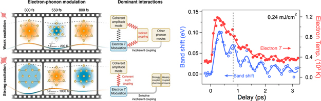
Figure 10. Coherently manipulating the charge and lattice orders and their interactions using light. After excitation by an ultrafast laser pulse, the electron temperature in a CDW material 1T-TaSe2 is modulated by the excited coherent phonon—by between 200 and 2000 K. In all past work, the electron bath cooled monotonically due to electron–phonon coupling. The dominant interactions also switch as the material enters a new 2D phase that cannot be reached via equilibrium routes. Reproduced with permission from [83].
Download figure:
Standard image High-resolution imageLight-induced spin manipulation: for more than two decades, ultrafast lasers have been used to quench or switch the magnetic state of materials (see sections 5 and 6 by Radu and Oppeneer for additional perspectives on experiments and theory in ultrafast magnetism) [93, 94]. To date laser-induced manipulation of the magnetic state has almost exclusively been understood as a secondary process taking place on picosecond timescales. We use a suite of correlated high harmonic based spectroscopies: trARPES, combined with HHG-based element-specific magneto-optic probes, to detect the excitations present in the material, over a full range of laser fluences and depths. As illustrated in figure 11 (left), we demonstrated that a femtosecond light pulse can directly transfer spin polarization from one element to another in a half-metallic Heusler material, Co2MnGe [95, 96]. This spin transfer initiates as soon as light is incident on the material, showing that we can spatially transfer angular momentum between neighbouring atomic sites on timescales < 10 fs. In yet another surprizing finding in Ni (figure 11, right), when the electron temperature is transiently driven above the Curie temperature, there is an extremely rapid change in the material response: the spin system absorbs sufficient energy within 20 fs to subsequently proceed through the phase transition, while demagnetization occurs on much longer, fluence-independent, timescales of ∼176 fs. These findings uncover a new timescale of ultrafast demagnetization and collectively show that previous theoretical understanding is incomplete. The addition of spin-resolved ARPES, and ultrafast soft x-ray and electron spectroscopies and imaging, can yield additional insight into ultrafast spin dynamics and transport.
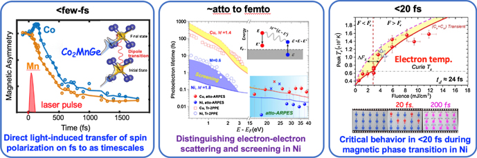
Figure 11. New timescales for spin manipulation observed experimentally. (Left) Light can transfer spin polarization between two elements in a Heusler alloy, on few-fs timescales. Reproduced from [95]. CC BY-NC 4.0. (Right) Ultrafast electron calorimetry showed that the energy required to drive a true magnetic phase transition in Ni is absorbed by the spin system within ∼20 fs, clearly observable as an inflection point in the measured electron temperature at the Curie temperature. 97(Centre) Distinguishing electron–electron scattering and screening in Ni. Reproduced from [86]. CC BY-NC 4.0.
Download figure:
Standard image High-resolution image7.4. Concluding remarks
Over the past 3 decades of studies of HHG, and 2 decades of developing new experimental methodologies using ultrashort pulse EUV light to study materials, we now have a set of tools with broad applicability, whose potential has to-date barely been tapped. As HHG sources become easier to use, they can proliferate to a larger variety of experimental venues, both to apply already-established techniques, and to develop new ones. The ability to coherently manipulate quantum materials, using HHG as a probe and expanding the use of a variety of complementary coherent techniques, would facilitate the development of many exciting areas of future investigation. For example, delicate control of coherent phonons with well-designed laser pulse sequences, or resonant driving of quantum materials with mid-IR and THz radiation, provide unprecedented opportunities to tune the material state and complex interactions. To better understand the response of quantum materials, a combination of HHG-based photoemission and magnetic spectroscopies, with structured EUV/x-ray scattering and diffraction methods, can give a comprehensive understanding of both the equilibrium as well as new light-induced properties of materials. The study of high harmonic quantum light science, and the applications for time-resolved studies in material, have shown an extraordinary potential for further advances and impact on broad fields of materials science.
Acknowledgments
We gratefully acknowledge support from the National Science Foundation through the JILA Physics Frontiers Centre PHY-1734006, and a Gordon and Betty Moore Foundation EPiQS Award GBMF4538, for the attosecond ARPES setups and methods. We gratefully acknowledge support from the Department of Energy Office of Basic Energy Sciences X-Ray Scattering Programme Award DE-SC0002002 for the spin dynamics setups and methods. We gratefully acknowledge support from the Department of Energy Office of Basic Energy Sciences AMOS Award DE-FG02-99ER14982 as well as an MURI Grant from the Air Force Office of Scientific Research under Award Number FA9550-16-1-0121 for the HHG light source setups and methods.
8. Ultrafast momentum microscopy—a new approach for ultrafast bandstructure imaging
Benjamin Stadtmüller
University of Kaiserslautern, Germany
8.1. Status
Over the last decades, time-resolved photoelectron spectroscopy has developed into one of the most powerful techniques to study electronic structure dynamics of condensed matter after optical excitation. In the so-called single particle excitation limit, the time-dependent photoemission current directly reflects the quasi-particle lifetimes of optically excited charge and spin carriers. This provides a direct view onto the fundamental energy and (angular-) momentum dissipation processes in materials. On the other hand, optically induced (spin-dependent) band structure renormalizations, such as band shifts, band gap renormalizations or band broadenings are spectroscopic signatures of optically induced phase transitions and non-equilibrium states of matter. The magnitude of these band structure changes is typically in the range of a few to several hundreds of meV depending on the class of materials and can be directly linked to the charge-, spin-, and orbital-dependent interactions of the many-electron system with its surrounding.
These enormous capabilities of time-resolved photoemission have been propelled over the last decades by the continuously evolving developments in photoemission detector technology and ultrafast light sources. In the early days of time-resolved photoemission, conventional photoemission spectrometers allowed one to record the energy dependent photocurrent at selected points in the band structure (see schematic illustration in the lower left corner of figure 12). This enabled groundbreaking studies that revealed the thermalization dynamics of electrons in metals [105] or the energy-dependent scattering of bulk and surface electrons [106–108]. At the beginning of the 21st century, novel hemispherical electron analysers emerged with 2D detector systems for parallel detection of energy and momentum of the photoelectrons (see upper left of figure 12) or with highly efficient spin detectors. They were the foundation that provided the first insights into the collective excitations of the electron and spin systems during the optical melting of charge and spin order in magnetic and correlated materials [109, 110] with a temporal resolution down to the sub-100 fs range. The latter is mainly determined by the temporal width of the laser pulses of the pump and probe beam which can nowadays be as short as a few tens of femtoseconds (see section 7 by Margaret M Murnane, Xun Shi and Henry C Kapteyn). Despite these achievements, we are still far away from harnessing the full potential of time-resolved photoelectron spectroscopy that could be simultaneously sensitive to the time-, spin-, momentum-, energy-, and spatially-resolved band-structure dynamics throughout the entire BZ.
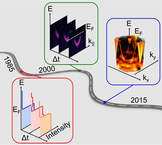
Figure 12. Evolution of the complexity of the spectroscopy information in time-resolved photoemission experiments over the last few decades.
Download figure:
Standard image High-resolution image8.2. Momentum microscopy for time-resolved photoelectron spectroscopy
The dream of such a complete photoemission experiment has recently been revived by a new breakthrough in ARPES known as momentum microscopy [111–113]. A momentum microscope is illustrated in figure 13. It takes advantage of an immersion lens column of a photoemission electron microscopy (PEEM) optics operated in momentum space mode to record the entire photoemission distribution above a sample surface. In combination with a dispersive or time-of-flight imaging energy analyser, it allows one to access the entire energy- and momentum-dependent photoelectron distribution above the sample surface in a single experimental geometry. For extreme UV photon energies, this allows to image the complete valence band structure of materials throughout their entire BZ (see upper right inset of figure 12) for fixed incidence angle of light. This, in turn, enables one to exploit dichroism- and light-polarization-induced effects in the momentum resolved photoemission experiments. Crucially, momentum microscopy can also be combined with imaging multichannel spin filters that conserve the full momentum-space information in the spin-filtering process [112, 113] thus allowing for a complete imaging of the spin-dependent band structure with utmost efficiency.
Figure 13. Schematic illustration of a momentum microscopy experiment. It consists of a PEEM optics and a dispersive (as shown here) or time-of-flight imaging energy filter.
Download figure:
Standard image High-resolution imageInspired by these extraordinary advances in conventional photoemission spectroscopy, momentum microscopy has also found its ways into the time-resolved photoemission community. This has resulted in the successful implementations of ultrafast (pump-probe) momentum microscopy experiments optimized for different types of ultrafast light sources. In the single particle excitation regime, time-resolved two-photon momentum microscopy [114] was introduced to access the momentum-dependent quasi-particle lifetime of optically excited electrons in the centre of the surface BZ using fs-laser light pulses in the visible range. Similarly, time-resolved momentum microscopy setups were combined with ultrafast light sources in the EUV or soft x-ray range. This paved the way towards imaging ultrafast band structure renormalizations or the (excitonic) charge carrier dynamics in molecular and novel quantum materials in an exceptionally large range of momenta and throughout their entire surface BZ [115–118].
8.3. Current challenges and future strategies
While these successful implementations have demonstrated the capabilities of time-resolved momentum microscopy, they have also unearthed challenges and limitations that must be overcome to unleash the full potential of this new technique. The most severe obstacle is space-charge effects. They limit the ultimate energy and momentum resolution as well as the signal-to-noise ratio (SNR) of the experiment. Despite being present in all time-resolved photoemission experiments, space-charge induced distortions of the photoelectron distribution are particularly crucial for time-resolved momentum microscopy. In particular, they can both occur by Coulomb repulsion of photoelectrons in vacuum in front of the sample surface as well as in the microscope column itself. The influence of space charge effects on the quality of the photoemission data can only be reduced by limiting the number of photoelectrons that are excited by each laser pulse. This approach, however, severely reduces the signal to noise ratio in the momentum microscopy data when reducing the average photon flux of the ultrafast light source at constant repetition rate. On the other hand, it can potentially result in a constant heating of the material when increasing the repetition rate of the ultrafast light source to compensate for the reduction of pump or probe photons per pulse [115]. This vicious circle can only be broken by novel innovative concepts for improving the momentum microscopy optics itself. Design criteria for such improvements have already been proposed recently [118] giving hope to overcome the instrumental induced space charge challenge in time-resolved momentum microscopy.
A second major obstacle is the sheer amount of spectroscopic information that can be obtained by time-resolved momentum microscopy. This requires the development of new data handling and data analysis schemes, which enable highly efficient online data screening during experiments as well as in-depth analysis afterwards. Looking on the bright side, the extensive spectroscopic information can pave the way towards yet unexplored data analysis procedures that could be based on pattern recognition algorithms, machine learning or big data analysis schemes [120]. This could potentially revolutionize band structure imaging and set the stage for uncovering novel band structure signatures beyond the conventionally investigated high-symmetry directions of materials in momentum space.
8.4. Concluding remarks
Undoubtedly, momentum microscopy has revolutionized many aspects of spin- and momentum-dependent photoelectron spectroscopy and has demonstrated its unique potential for time-resolved band structure imaging of materials in exceptionally large ranges of energy and momentum space. However, it still needs to be seen whether momentum microscopy can replace hemispherical electron analysers as next-generation ultrafast band structure imaging tool. First, it needs to prove its capabilities for time-resolved band structure imaging of novel materials beyond mere model systems. This will be the necessary starting signal to begin focussing on further degrees of freedom such as the spin or spatially-dependent band structure dynamics. This will open new avenues towards exploring ultrafast phenomena and optically induced transitions in novel quantum materials or stacked and twisted 2D systems that can nowadays only be grown on the micrometre scale.
Acknowledgments
I thank Benito Arnoldi for his support in designing the figures of this article and acknowledge financial support by the Deutsche Forschungsgemeinschaft (DFG, German Research Foundation)—TRR 173—268565370 (project A02).
9. Time-resolved photoemission spectroscopies of 2D semiconductors and their heterostructures
Keshav M Dani1 and Felipe da Jornada2
1Okinawa Institute of Science and Technology Graduate University, Japan
2Stanford University, United States of America
9.1. Status
Photoemission spectroscopy techniques—wherein one photoemits an electron from a material using a high-energy photon and studies its properties—can provide unparalleled insight into materials and condensed matter systems. Among these, two particularly powerful and complementary techniques exist: with ARPES, the kinetic energy and emission angle of the photoemitted electron provide direct knowledge of the electronic structure of the material [121]; on the other hand, PEEM images a material's surface in real space and can deliver detailed knowledge about surface morphology, electronic and chemical properties, and magnetic structures with nanometer-scale spatial resolution [122].
Over the past few decades, the merger of techniques of photoemission spectroscopy with ultrafast spectroscopy have brought in the temporal dimension. In such schemes, first a femtosecond pump pulse, typically in the visible-near infrared range, excites the sample. Thereafter, a time-delayed femtosecond probe pulse in the UV–XUV photoemits electrons from the photoexcited sample. As in the case of static measurements, this photoemitted electron can be resolved in energy, momentum (ARPES) or real-space (PEEM). By assembling the data taken at different time-delays, one obtains powerful visuals of the system dynamics after photoexcitation.
Photoemission spectroscopy techniques, which are largely surface sensitive, have found an ideal partner in 2D materials, where the absence of the third dimension makes the measurements and their interpretation easier. Among the 2D materials, semiconductors and semi-metals constitute an important sub-class, where time-resolved (TR) photoemission studies are very relevant due to the significance of their optically excited states for science and technology [124].
However, studying 2D semiconductors, such as monolayers of TMD, via time-resolved photoemission spectroscopy has proven to be experimentally challenging. For TR-ARPES, more studies have been performed on bulk TMDs, where the availability of large-area, high-quality samples and increased photoemission signal makes the experiments easier. However, studies on bulk TMDs are not a substitute for their atomically thin versions, due to critical differences in electronic structure, optical properties, electronic screening, and proposed applicability for opto-electronic technologies.
For TR-PEEM, studies on 2D semiconductors have been even more challenging. Even for traditional semiconductors, TR-PEEM measurements are a relatively recent achievement [123], which were followed by some initial results in 2D materials [127–129].
Beyond the early results in TR-ARPES and TR-PEEM, a rich world of scientific exploration awaits, one that likely requires a merger between these two, hitherto disparate, fields.
9.2. Current and future directions/challenges
Time-resolved ARPES. While the first few TR-ARPES studies in monolayer TMDs [125, 126] have observed free photocarrier dynamics, the grand challenge remains to observe the strongly bound excitonic states which arise due to the weak electronic screening in 2D.
Since the 1950s, the relative electron–hole momentum has played a key role in the description and understanding of excitonic properties. However, since excitons have mostly been studied using optical techniques, the momentum degrees of freedom of the bound electron and hole have remained unavailable, with only a few notable exceptions [139, 140]. A slew of recent theoretical studies [135, 136, 138] have proposed resolving the momentum degrees of freedom in an exciton using TR-ARPES. By photoemitting the bound electron and measuring its momentum, one could directly distinguish the different excitonic states (e.g. bright excitons, dark excitons, hot excitons), reveal their properties, and understand their role in the dynamics after photoexcitation. This would constitute critical knowledge for proposed opto-electronic technologies in monolayer TMDs. Next, one could directly probe the nature of the electron–hole bond in the exciton, imaging the excitonic wavefunction in real- and momentum-space, and observing the long predicted anomalous dispersion relationship: the photoemitted bound electron exhibits the negative dispersion and mass of its hole-partner, instead of the positive dispersion of a free electron (figure 14). With TR-ARPES, one can also directly access dynamical processes such as exciton–phonon scattering and exciton–exciton scattering in momentum space. These processes, fundamentally different and more complex than their free-electron counterparts, have been theoretically described over the past several decades, but remain experimentally unavailable. In the course of preparation of this chapter, TR-ARPES experiments on microscopic samples of monolayer WSe2 have indeed been successful in observing the bright and dark excitonic states [117], in imaging the excitonic wavefunction and in observing the elusive, anomalous dispersion relationship [141].

Figure 14. Schematics of a TR-ARPES setup to probe an exciton. (a) Merging ultrafast techniques with photoemission spectroscopy: a visible pump pulse excites the sample at zero-delay, followed by a time-delayed XUV probe pulse to photoemit electrons. The photoemitted electrons are resolved in energy, momentum and real space, as a function of time-delay to obtain movies of the electron dynamics in µ-ARPES mode, or momentum-resolved PEEM mode. (b) Within a Wannier picture and a two-band model, an exciton |X⟩ with zero center-of-mass momentum (left) can be described as a linear combination of electron–hole pairs (right). (c) An ultrafast XUV probe in an TR-ARPES experiment setup probes a particular conduction electron with a given energy and momentum, thus leaving behind one of the holes that make up the exciton. For an initial exciton with zero center-of-mass momentum, larger momenta k are associated with higher-energy holes (lower-energy valence electrons), and hence the kinetic energy of the photoemitted electron decreases with increasing k. (c) The apparent photoemission spectrum associated with photoemitting an electron from an exciton displays a characteristic negative dispersion which follows the dispersion of the valence electron that is left behind during the XUV probe.
Download figure:
Standard image High-resolution imageBeyond the observation of excitons in monolayer TMDs, questions immediately arise regarding the TR-ARPES signatures (and dynamics) of other exotic few-particle states, such as trions, biexcitons, and exciton polarons.
Beyond monolayer TMDs, TR-ARPES measurements in other 2D heterostructures, such as bilayer graphene and twisted TMDs, could be used to probe unusual ground states and their interaction with light to form novel elementary excitations, such as the interlayer exciton and exciton insulators. Additionally, time-resolved techniques also allow one to explore and characterize metastable electronic configurations, such as optically driven Floquet states in topological insulators and Floquet–Weyl phases in 3D Dirac semimetals.
Time-resolved PEEM. In addition to angle-resolved photoemission experiments, nanoscale spatially resolved studies via PEEM also offer powerful and complementary insights into the properties of 2D semiconductors. The grand challenge in this context is to obtain static and time-resolved PEEM images of monolayer TMDs with nanoscale spatial resolution and meV-scale energy resolution, using only specific photoemitted electrons, such as those from the vertices of the BZ, or those bound in different excitonic states. Since 2D semiconductors are quite susceptible to small changes in the local environment, such images would provide powerful information on the spatio-temporal variations in energy and occupation for the specific electronic states probed. On the one hand, this will help to eliminate unwanted sample heterogeneity, thus facilitating the fabrication of larger, higher-quality samples for science (like the TR-ARPES studies described above), or future device technology. On the other hand, such studies could be crucial for realizing proposals to engineer 2D materials on the nanoscale by manipulating the local dielectric environment [130] or through strain engineering [131].
Beyond monolayer TMDs, TR-PEEM could offer an alternate route to study Moiré physics in twisted TMD heterostructures by directly accessing the nanoscale periodicity in space. Similarly, TR-PEEM could study interesting spatio-temporal dynamics occurring near the interfaces of lateral heterostructures. Finally, the possibility of single-shot TR-PEEM imaging of multiple electrons could access electron–electron correlations in space and time between photocarriers.
9.3. Advances in science and technology to meet challenges
Experimental advances. While the path ahead in time-resolved photoemission spectroscopies of 2D materials is alluring and rich with the promise of new scientific discoveries, it is fraught with experimental and theoretical challenges.
Critically, time-resolved photoemission studies of 2D materials require ultrafast XUV photons to access the interesting physics at the vertices of the BZ. Synchrotrons easily provide XUV photons, but they typically lack time resolution. Table-top setups can deliver the time-resolution, but they typically suffer from poor photon flux. Continued advances in delivering a large flux of ultrafast XUV photons, at high repetition rates to minimize space-charge effects, are necessary (see section 7 by Margaret M Murnane, Xun Shi and Henry C Kapteyn). For TR-PEEM there is an additional constraint—the requirement of forming an image with nanometer-scale resolution necessitates a large flux of ultrafast XUV photons per unit area.
Next, for TR-ARPES studies of few-layer TMDs, one needs to exclusively probe small, micron-scale regions of the sample, where the number of layers is constant, i.e. TR-μ-ARPES. In addition, the ARPES studies described above, such as imaging of the exciton wavefunction, require measuring the full 2D BZ of the monolayer TMD. Both these issues can be solved by incorporating PEEM-based technology into the ARPES measurement, often referred to as momentum microscopy (see section 8 by Benjamin Stadtmüller). Similarly, for TR-PEEM, the need to only image photoelectrons from specific regions in the BZ brings in angle-resolution considerations to PEEM measurements. While some of these instrumentation capabilities are now available [142], further development is continuously occurring to combine and enhance more aspects of photoemission spectroscopy, including the tantalizing possibility of adding spin-resolution to the mix [132].
Finally, inhomogeneous broadening in the sample is likely a major factor in limiting sophisticated measurements of photoexcited states (particularly long-lived ones) with high energy resolution. While photoluminescence experiments on 2D semiconductors now regularly achieve few meV linewidths, ARPES studies on few-layer TMDs suffer from very broad linewidths. Improvements in sample quality, in the context of photoemission spectroscopy, is very important.
Theoretical advances. Besides the advances and challenges required in experiment, substantial developments in theory are required to understand the photoemission spectroscopic signatures in low-dimensional materials, especially given the variety of single- and multi-particle states which can be created. Since such experiments probe systems in their excited electronic configuration, it is natural to describe them via equilibrium Green's-function approaches, such as the ab initio GW approach for describing quasiparticle excitations and the ab initio GW plus BSE approach for excitons. The dynamics of Wannier excitons near equilibrium has also been successfully parametrized in terms of Bloch states, often providing important insights of the exciton dynamics of novel 2D material [135, 137, 138]. However, such techniques are not applicable for systems far from equilibrium, as is often the case for TR-ARPES, when the dynamics of photoexcited carriers may dramatically change the many-electron interactions. The natural generalization is to employ the KBE, which is a rigorously exact formalism to describe systems out of equilibrium. In practice, approximations are required when simulating real materials, since one needs to propagate two-time Green's functions, of the form G(r, r'; t, t'), instead of the equilibrium, single-time Green's function G(r, r'; t − t'). To tackle this, recent approaches typically approximate the many-body electron–electron interactions as instantaneous (i.e., they neglect memory effects) [133] and hence only require to evolve a much simpler time-diagonal Green's function G(r, r'; t). Such approximations have been used to understand linear and higher-harmonic absorption processes, shift-current conductivity, and optically driven exciton-insulator ground states.
Going forward, first, one needs to properly account for memory effects, which are important when dealing with strong pump excitations, and are related to the physics of photocarrier-induced change in the electronic screening, dynamical renormalization of the bandgap and exciton binding energy, exciton Mott transitions, etc. The community will likely need to study the KBE with approximations such as the generalized Kadanoff–Baym ansatz. Secondly, given the interest in excitons in quasi-2D TMDs, it is necessary to accurately capture their dynamics and dephasing from first principles, which is hard to access with the standard KBE for the single-particle electronic Green's function. Instead, it is much more natural and conceptually simpler to study such processes employing a two-particle non-equilibrium Green's function approach—or even higher-order Green's function to study nonequilibrium phenomena involving trions and biexcitons—, though they are computationally much more involved and corresponding ab initio approaches are still incipient [134, 135]. Still, the possibility of characterizing novel materials and predicting qualitatively new metastable electronic phases tunable by light makes this development an exciting and timely direction.
9.4. Concluding remarks
The advent of time-resolved photoemission spectroscopies have the potential to offer powerful and insightful views into the detailed dynamics in condensed matter systems, as well as the complex nature of states that form after interaction with intense light. In 2D semiconductors, rich avenues of scientific exploration await, but need further advances in ultrafast XUV optics, multi-dimensional photoelectron spectroscopy, and high-quality sample fabrication for photoemission studies. With the level of experimental sophistication that can be achieved, theoretical advances that account for memory effects after photoexcitation, and employ multi-particle non-equilibrium Green's function approaches, are necessary to fully understand the measured phenomena.
Acknowledgments
KMD thanks Ting Cao, Mack Kira, Michael Man, Julien Madeo and Vivek Pareek for discussions. KMD thanks Vivek Pareek for help with figure preparation. FHJ thanks Yang-hao Chan and Diana Y Qiu for discussions.
10. Ultrafast nanooptics and plasmonics by time-resolved photoemission electron microscopy
Eva Prinz and Martin Aeschlimann
University of Kaiserslautern, Germany
10.1. Status
Surface plasmons enable the localization of light below the free space diffraction limit at optical frequencies, making plasmonics an active research field presenting a variety of technological applications, ranging from cancer treatment to improved photovoltaic cells. Two different plasmonic modes can be excited by ultrashort light pulses:
- (a)Localised surface plasmons (LSPs) in metal nanostructures. These are coherent oscillations of the whole conducting electron gas that result in strongly enhanced electromagnetic near-fields.
- (b)Propagating surface plasmon polaritons (SPPs) along metal–dielectric interfaces. On flat surfaces, SPPs cannot decay radiatively due to the momentum mismatch between SPPs and light, which leads to long coherent lifetimes and propagation lengths of hundreds of micrometers. For the same reason, SPPs cannot be excited directly with light. Instead, either evanescent waves or structures such as slits and gratings allow the momentum mismatch to be overcome.
To observe the dynamics of plasmonic fields, a measurement technique that combines subfemtosecond temporal and nanometer spatial resolution is needed. For this, time-resolved photoemission electron microscopy (TR-PEEM) has been established as a powerful ultrafast spectroscopy tool that fulfils all the requirements [143]. Commonly, plasmons are excited with an ultrashort pump laser pulse and their dynamics are probed with a second pulse in a two-photon photoemission process. In addition, many PEEMs also allow for energy-resolved measurements. This feature aided, for example, in the investigation of the so-called plasmoemission, where electrons are emitted from a metal surface in a nonlinear process purely by the absorption of SPPs, without an involved light field. By using energy-resolved PEEM, different orders of plasmoemission could be separated [144] (figures 15(a)–(c)).
Figure 15. (a) Sketch of multiplasmon plasmoemission from focussed SPPs. (b) Energy-filtered plasmoemission based PEEM images of the focus spot at energies corresponding to different emission orders. (c) Corresponding simulation results. (d) Scanning electron microscope (SEM) image of nanodisk dimers. (e) Corresponding time-resolved photoemission intensities with fitted dephasing times, measured for different disk distances. (f) SEM image of a plasmonic Archimedean spiral lens (of the order m = 10) for the generation of vortices with OAM. (g)–(i) TR-PEEM images of a rotating plasmonic vortex within a single optical cycle. (a)–(c) Reprinted with permission from [144]. Copyright (2017) American Chemical Society. (d) and (e) Reprinted figure with permission from [149], Copyright (2020) by the American Physical Society. (g)–(i) From [148]. Reprinted with permission from AAAS.
Download figure:
Standard image High-resolution imageTR-PEEM is also commonly used for the study of LSP lifetimes at nanostructures [145] and for the real-time observation of SPP propagation [146]. However, at a light incidence angle of 65–74°, as it is generally used (with this grazing-incidence geometry, the light beam passes by the electron optics column), just a beating pattern of the SPP and light field is recorded. Thus, the development of the first normal incidence (NI-)PEEMs in 2014 [147] in order to provide a direct descriptive visualization of SPP wave packets propagating across a metal surface was a significant breakthrough. Normal incidence can be realized with two different methods: either by inserting a small mirror in the back focal plane of the objective lens, as close to the photoelectron path as possible, or by the use of a magnetic beam splitter (sector field) that deflects the electron sideways into the imaging column.
This direct visualization of SPP wave packets in attosecond time-steps was used e.g. to record the revolution of plasmonic vortices with orbital angular momentum (OAM) that allowed determining high-order OAM for the first time [148] (figures 15(f)–(i)). Plasmonic vortices have promise in delivering high-order angular momentum quanta to electronic degrees of freedom, and can also be used as tweezers for particle manipulations.
In addition, an NI-PEEM set-up has been used to study the near-field enhancement and dephasing times of only a few femtoseconds of LSPs at plasmonic nanoantennas [149] (figures 15(d) and (e)).
10.2. Current and future challenges
For the development of new plasmonic applications, specifically designed plasmonic structures are required. In this section, different promising examples will be presented that could be solely investigated with the temporal and spatial resolution provided by TR-PEEM.
Due to their unique properties, SPPs enable radiation-free coherent energy transfer and they can be used to excite LSP resonances [150]. In an elliptical cavity with two whispering-gallery-mode (WGM) nanoantennae, the delocalized SPPs were combined with LSPs, periodically transferring energy from one selectively excited antenna to the other [151] (figure 16(a)). When the WGM antennae are separated by twice the wavelength of the exciting light, the energy transfer rate is similar to free-space coupling over a distance of only 10 nm. This opens new perspectives for long-range quantum emitter coupling and mesoscopic energy transfer.

Figure 16. (a) SEM image of an elliptical SPP cavity with two WGM antennas embedded at the two focal points of the cavity. The illumination condition for a TR-PEEM to observe periodic energy transfer between the antennas is indicated. (b) Schematic of a plasmonic lens switchable by UV light with two possible focus spots. (c) PEEM images with a photon energy of 3.1 eV in a hexagonal magneto-plasmonic crystal for different polarization states as indicated. (a) Reproduced from [151]. CC BY-NC 4.0. (b) Reprinted with permission from [152]. Copyright (2015) American Chemical Society. (c) Reprinted with permission from [155]. Copyright (2016) American Chemical Society.
Download figure:
Standard image High-resolution imageAnother intriguing implementation of a plasmonic switch uses a gold substrate coated with a polymer film doped with photochromic molecular switches that enable a UV-light induced reversible change of the SPP group velocity [152]. By combining this functional interface with a plasmonic lens, the SPP focus can be controlled and used as a plasmonic switch (figure 16(b)). Alternatively, a switching of the focus spot can also be achieved by utilizing the plasmonic spin-Hall effect that leads to different spot positions depending on the pumping light's helicity [153].
A different, promising approach utilizes polarization-sensitive metasurfaces composed of nanoslits. When arranged in an Archimedean spiral and excited by a femtosecond laser pulse at resonant frequencies, rotating SPP vortices with OAM are created, while the orientation of the nanoslits offers a new degree of control over the plasmonic OAM dynamics [154]. It is possible to make the originally chiral Archimedean spirals (that create light-spin dependent OAM) achiral, which leads to the formation of light-spin independent vortices. Alternatively, the amount of plasmonic OAM and the rotation direction of the vortices can be controlled, which can be especially useful by offering additional flexibility in plasmonic tweezer applications.
Lastly, the rapidly growing field of magneto-plasmonics aims to combine magnetic and plasmonic functionalities. It has been shown that on a nanopatterned ferromagnetic nickel surface that supports SPPs, the electric near-field can be controlled by tuning the polarization state or the photon energy of the incident light [155] (figure 16(c)). This effect is directly correlated to the excitation of SPPs and the enhancement of the polar magneto-optical Kerr-effect, introducing the concept of a magneto-plasmonic metastructure and opening new routes for the design of functional plasmonic systems.
While all the studies presented here led to many new insights and aided the design of functional devices, recent technological and methological advances that are presented in the next section open the door towards an even deeper understanding in the field of plasmonics.
10.3. Advances in science and technology to meet challenges
In recent years, the concept of so-called atto-PEEM that probes the ultrafast near-field oscillations on their native attosecond time scale has gained great interest [156] as it promises new insights into the physics of plasmonic eigenmodes. The proposal is based on attosecond streaking spectroscopy, where a few-cycle near-infrared femtosecond pump pulse excites LSPs and the temporal evolution of the plasmonic field is subsequently probed by a single XUV attosecond pulse that is created via HHG (see section 7 by M Murnane et al).
To successfully implement atto-PEEM, a variety of technological and fundamental challenges that must be overcome are currently being addressed. With a pulse duration of a few hundred attoseconds or even less, the energetic spectrum of the XUV pulses has an FWHM of 10 eV or more which negatively affects both the imaging contrast and the achievable spectral resolution. Also, to avoid space charge effects that are caused when too many photoelectrons are created in a single excitation event, the used intensity of the pump and/or probe pulse must be severely limited. This makes the low repetition rates of 10 kHz or less of the laser sources that are commonly used for HHG generation one of the most important challenges to resolve since it is hard to maintain the necessary temporal stability during the time that is required for the acquisition of an atto-PEEM image. Fortunately, the recent development of fibre laser systems that offer significantly higher repetition rates in the MHz range was a major step towards establishing atto-PEEM as a new time-resolved technique. In addition, a novel scheme makes use of a sample rear side pump and front side probe illumination geometry that further reduces the space charge problem [157].
Another challenge that calls for the implementation of new technologies is the investigation of plasmon-generated hot carriers. This offers many opportunities for fundamental research and in applications such as photon harvesting. For the construction of new devices for plasmonic energy conversion it is essential to understand the differences between photo-induced and plasmon-induced hot electrons. Ultrafast TR-PEEM is uniquely suited for the detection of differences in the electron's energy and even momentum distributions. It not only allows for both the temporal and spatial separation of SPPs and light pulses (in the case of LSPs, only a temporal separation is possible) but can also be used as a momentum microscope by adjusting the settings of the electrostatic or magnetic lenses to image the Fourier transform of the real space image onto the detector. An open very fundamental question is whether there is a difference in the energy and momentum distribution of hot electrons that were either excited directly by light or due to plasmon decay.
The most recent methodological breakthrough in TR-PEEM is the successful implementation of time-resolved vector microscopy. This approach employs two probe beams with distinct but different light polarizations to access the dynamics of all vector electric field components of plasmonic waves and not merely their intensity distribution. This offers a unique opportunity for imaging the evolution of topological plasmonic quasiparticles, such as skyrmions and merons [158, 159], for instance to uncover the time-dependent experimental skyrmion numbers [158]. It also could be the decisive tool towards an unprecedented understanding of topological nanophotonic systems in space and time.
10.4. Concluding remarks
The near-field sensitive TR-PEEM technique, offering nanometer spatial and subfemtosecond temporal resolution, is an ideal tool for the investigation of a variety of plasmonic phenomena. These range from fundamental properties of SPPs and LSPs, such as plasmoemission, rotating SPP vortices with an OAM, resonances at nanoantennas, the plasmonic spin-Hall effect, and topological plasmonic fields, to functional designs for future applications like the coupling of LSPs and SPPs for radiation-free energy transfer, surfaces with switchable dielectric properties, metasurfaces, and magneto-plasmonic crystals. In addition, many PEEMs also allow for energy-resolved measurements and can also be used as momentum microscopes. These features, together with emerging novel light sources such as XUV attosecond pulses generated via HHG pave the way towards exciting future discoveries and fundamental insights in the field of ultrafast plasmonics and the development of novel miniaturized devices.
Acknowledgments
EP acknowledges support from the Max Planck Graduate Center at the Johannes Gutenberg University Mainz through a PhD fellowship.
11. Ultrafast spectroscopy of hybrid metal halide perovskites
Rebecca L Milot
University of Warwick, United Kingdom
11.1. Status
Hybrid metal halide perovskites (figure 17(A)) are a class of hybrid organic–inorganic semiconductors that have shown great promise for use in a number of optoelectronic devices, most notably photovoltaic cells. High quality perovskite thin films are easily synthesized with simple starting materials and have therefore been hailed as potential alternatives to traditional semiconductors such as silicon or GaAs, which require harsher and more stringent synthesis conditions. Furthermore, the band gap absorption onset of perovskites is highly tuneable with simple chemical substitutions (figure 17(B)) and can therefore be tailored to maximize the efficiency for specific applications such as tandem solar cells, LEDs, lasers, or photodetectors [160]. As these materials have developed rapidly over the last decade, ultrafast spectroscopy has played an important role in analysing charge transport mechanisms and has thus contributed greatly to informed device design.

Figure 17. (A) Cubic crystal structure of methylammonium lead triiodide (CH3NH3PbI3), the prototypical metal-halide perovskite. Hybrid metal halide perovskites demonstrate the classic AMX3 perovskite structure, where A is an organic cation such as methylammonium or formamidinium (FA), M is a divalent metal cation such as Pb2+ or Sn2+, and X is a halide. (B) Thin films of mixed halide FA lead perovskites demonstrating the tunability of the band gap with halide composition. Reproduced from Eperon et al 2014 Energy Environ Sci. 7(3) 982–8 with permission from the Royal Society of Chemistry. (C) A diagram of a perovskite solar cell. Light is absorbed by the perovskite layer and charge carriers then diffuse to the electron- and hole-transport media (ETM and HTM, respectively). The optically transparent electrode typically consists of a conducting oxide layer deposited on glass, and a layer of gold serves as the counter electrode. Reprinted with permission from [160]. Copyright (2016) American Chemical Society
Download figure:
Standard image High-resolution imageIn perovskite thin films, many of the optoelectronic processes essential for efficient device performance occur at ultrafast timescales. Within femtoseconds to nanoseconds following photoexcitation, charge-carriers encounter a range of energy loss possibilities including cooling of hot carriers, recombination events, and interactions with the lattice. Although other processes can occur at much longer timescales, these initial ultrafast processes have the potential to impose an upper limit on the efficiency of the entire device, and ultrafast probes are thus essential for characterizing these dynamics [161]. As perovskites have spectroscopic features ranging from the terahertz to the visible frequencies, a variety of ultrafast techniques have been employed including time-resolved photoluminescence (TRPL) spectroscopy, ultrafast pump-probe techniques such as THz spectroscopy and visible and infrared TA spectroscopies, ultrafast coherent spectroscopies, and surface techniques such as sum frequency generation and ultrafast photoemission microscopy [160–164]. Although the majority of studies have focussed on isolated perovskite thin films, studies of full or partial devices will be of increased importance as the field progresses [161]. The discussion below summarizes some of the main results obtained thus far for isolated films and highlights potential for additional studies.
When perovskites were first incorporated into solar cells, the hybrid organic–inorganic nature of the materials led to an uncertainty as to whether the main charge-carriers were excitons as in organic semiconductors or free electrons and holes as in inorganic semiconductors. Initial ultrafast measurements of photoconductivity and PL dynamics supported the idea that the majority species are free electrons and holes, with moderate combined charge-carrier mobilities in the range of 10–50 cm2 V−1 s−1 [160, 165]. These measurements demonstrated the feasibility of a planar heterojunction device design, steering the field away from its initial design based on the dye-sensitized solar cell towards its current norm (figure 17(C)). Subsequent studies have suggested the charge-carriers may exist as large polarons, but these results are consistent with a largely free charge-carrier model [165].
Although excitons are a minority species at room temperature in many common perovskite materials, understanding the interplay between excitons and free charge carriers will be important for refining the picture of charge transport [161]. Additionally, there has been an increasing interest in 2D perovskites and perovskite nanocrystals, where increased exciton binding energies make excitons the majority carrier. Although charge-carrier lifetimes are shortened and effective charge-carrier mobilities are decreased as a result, these undesirable properties can be tuned synthetically [160, 163]. For both material classes, investigations are ongoing to fully characterize excitonic effects and their influence on charge transport and device efficiency.
Ultrafast spectroscopy has also aided in understanding deactivation process following photoexcitation, including charge-carrier cooling and charge-carrier recombination. Charge-carrier recombination dynamics, which have been investigated by several ultrafast techniques, are generally modelled by a simple rate equation
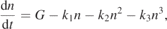
which expresses the rate of change of the carrier density n in terms of a generation rate G and monomolecular, bimolecular, and Auger recombination rate constants (k1, k2, and k3, respectively). Most work has focussed on understanding monomolecular and bimolecular recombination mechanisms, with fewer reports and less consensus on generation mechanisms (e.g. carrier cooling and exciton dissociation) and very limited information about Auger recombination.
Monomolecular processes generally involve carrier trapping with defect sites and are the dominant loss mechanisms in solar cells where charge-carrier densities are typically on the order of 1014 to 1015 cm−3 under operating conditions. The doping in perovskites thin films is generally unintentional and therefore largely uncharacterized a priori, and some of the only information about defect densities and energies comes from ultrafast measurements. Furthermore, degradation, light illumination, and ion migration can alter the defect chemistry, often complicating the analysis [162]. In perovskite thin films, monomolecular lifetimes have been found to encompass a wide range of values from picoseconds to microseconds, pointing to a large variability in defect concentration and activity between samples (see figure 18(A)). However, values on the order of 100 ns and above give suitable diffusion lengths to enable efficient charge transport at solar illumination intensities [166]. Ultrafast microscopy measurements have shown both energetic and spatial variations in charge-carrier dynamics, highlighting the complex nature of the defects in perovskites and the need for continued study in this area [164].
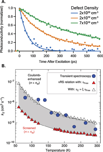
Figure 18. (A) An example of the variability of monomolecular recombination with defect density. For a series of FA tin triiodide (FASnI3 thin films), lifetimes of 59–590 ps are determined using optical pump/THz probe spectroscopy (OPTP) for defect densities ranging from 7 × 1018 cm−3 to 2 × 1020 cm−3. Reproduced from Milot et al 2018 Adv Mater. 30(44) 1804506. CC BY 4.0. (B) Bimolecular recombination rate constant k2 determined from OPTP measurements (blue circles) as compared to k2 calculated via the van Roosbroeck–Shockley relation and fits to the stead-state absorption spectra. Reproduced from Davies et al 2018 Nat Commun. 9 293. CC BY 4.0.
Download figure:
Standard image High-resolution imageContrasted to monomolecular recombination, bimolecular recombination is an intrinsic property of the material that involves radiative recombination between electrons and holes. It is thus essential for understanding the potential for light-emitting devices but also places an upper limit on charge-carrier diffusion lengths [166]. Due to photon recycling and diffusion effects, the exact values of k2 are difficult to summarize, but effective k2 values have been reported to range from 10−11 to 10−9 cm3 s−1 [166]. These values suggest that bimolecular recombination should not significantly limit charge-carrier diffusion at solar intensities but that carrier densities of 1017 to 1018 cm3 are needed to maximize radiative efficiency for light-emitting devices. Subsequent investigations have shown that an inverse absorption model can accurately describe temperature trends in k2 values determined by ultrafast spectroscopy (figure 18(B)), further emphasizing the similarities between perovskites and standard semiconductors such as GaAs [167]. As there are still many unanswered questions in this area such as the influence of polarons and lattice interactions [168], work to understand bimolecular recombination is ongoing and will be of increased importance as the development of light-emitting devices progresses.
In addition to interactions with each other, interactions of charge-carriers with the perovskite lattice have also been shown to influence charge transport efficiency by affecting both the exciton binding energy and charge-carrier mobility [169]. Perovskites have strong phonon modes at THz frequencies due to metal-halide lattice vibrations. For both lead- and tin-based materials, these modes were found to put an upper limit on the charge-carrier mobility, helping to explain why perovskites have lower charge-carrier mobilities than other inorganic semiconductors [165]. However, these phonon modes may assist in screening Coulomb interactions, preventing the formation of excitons, and thus allowing for free-charge-carrier transport at ambient temperatures [169]. Vibrations of organic cations could also have an effect on exciton binding energy, charge-carrier mobility, bimolecular recombination, and hot carrier cooling, but further investigations are needed to determine the extent of these effects [169, 170].
11.2. Current and future challenges
Although much has been learned about perovskite optoelectronics in the last decade, there are still several challenges to overcome, both fundamental and more device-specific, which ultrafast spectroscopy has the potential to address.
A main fundamental challenge remaining is to more fully refine the picture of charge transport in order to better understand the roles that excitons, polarons, and lattice vibrations play and what influence, if any, they have on device efficiency. These effects have proven difficult to characterize with one ultrafast technique alone, often resulting in conflicting evidence reported in the literature. The solution to this problem will require careful comparisons between different techniques and further investigation, for instance with ultrafast coherent spectroscopy methods, which can identify coupled states and thus help clarify coupling mechanisms [171].
A challenge that has existed since perovskites were first identified for use in solar cells has been characterizing the chemical identity, energetics, and densities of defect states [165]. Although ultrafast techniques have documented the effects of defects on recombination lifetimes, a full characterization of the chemical properties of the thin films to support these analyses is often lacking, although microscopy studies are beginning to make progress in this area [164]. To fully solve this problem, however, synthetic advancements are needed to controllably dope materials so that the effects of known defects can be benchmarked with ultrafast spectroscopy and compared to unintentionally doped samples.
One common criticism of ultrafast research in the perovskite field is that ultrafast techniques tend to probe local effects at timescales that are largely irrelevant to device operation. Although largely a marketing problem, this criticism is partially valid as measurements on isolated thin films can ignore a range of interface and surface effects due to the interaction of the perovskite thin film with other components of the cell (see figure 17(C)). To address this issue, ultrafast measurements must be performed under conditions more closely resembling devices. Encouragingly, some work has begun to analyse ultrafast processes in full devices and related structures [161]. As with initial perovskite research, analysis of these processes will at first be complicated due the inherent variability of the quality of perovskite thin films and devices. However, these investigations will present an opportunity to better understand the many physical processes occurring in devices and further justify the use of ultrafast measurements for this purpose.
11.3. Concluding remarks
Ultrafast measurements of charge-carrier dynamics and lattice interactions have been an essential part of the development of the field of perovskite optoelectronics. This influence is expected to continue as the devices are developed commercially, highlighting to a wider audience the potential of ultrafast measurements to aid in device characterization.
Acknowledgments
Thank you to James Lloyd-Hughes for useful discussions during the preparation of this manuscript.
12. Ultrafast dynamics of excitons and free charges in carbon-based 1D van der Waals heterostructures
James Lloyd-Hughes and Maria Burdanova
University of Warwick, United Kingdom
12.1. Status
Carbon nanotubes (CNTs) have formed a rich and fertile research field over the last two decades, and ultrafast spectroscopy has played a prominent role in uncovering the fundamental optoelectronic properties of these 1D materials. With the rise of atomically-thin 2D materials in recent years, the materials community has placed renewed importance in exploring how the vdW force can bind dissimilar compounds together into heterostructures, producing composites with tailored properties. In this contribution we highlight the importance of ultrafast spectroscopy for a broad class of carbon-based 1D vdW materials, including CNT bundles and composite heterostructures containing CNTs and transition metal dichalcogenides (TMDCs). We begin, however, by discussing the historical successes of, and challenges faced in, the ultrafast spectroscopy of CNTs.
In nanomaterials the low effective dielectric constant results in stronger Coulomb interactions than found in bulk semiconductors, thereby promoting the formation of many-body quasiparticles such as excitons and trions. For CNTs, exciton binding energies in the 200–500 meV range result in rapid exciton formation at room temperature, even after non-resonant excitation [172]. Ultrafast TA spectroscopy, TRPL spectroscopy, and optical pump, THz probe spectroscopy have all played major roles in elucidating the current, complex picture of exciton dynamics in CNTs [172–176]. Various processes contribute at different times after exciton formation, from fast, efficient exciton energy relaxation through the continuum of electron and hole states (within 100 fs), to exciton trapping (timescales of ∼10–100 ps) and slower radiative lifetimes (∼1 ns). Although excitons have large electric dipole moments for absorption, CNTs typically feature relatively weak photoluminescence (PL) as a result of efficient non-radiative processes, including exciton relaxation to optically-dark singlet states below the bright exciton singlet state.
Advances in the understanding of the photophysics of excitons in CNTs have progressed hand-in-hand with improvements in sample quality, as long, chirally-enriched, isolated CNTs become increasingly available. However, and somewhat counter-intuitively, greater sample homogeneity has led to more complex dynamical processes being uncovered, rather than revealing simpler trends. For instance, non-exponential (power law) exciton dynamics were identified in (6, 5) CNTs, linked to the trapping of dark excitons [173]. Time-resolved PL on single CNTs, rather than on an ensemble, uncovered substantially different monoexponential lifetimes for tubes with the same chirality, while excitonic dark states produced biexponential dynamics [172]. With long diffusion lengths (>100 nm) excitons are very mobile along the CNT axis, and variations in the number of defects on each individual CNT may account for the tube-to-tube changes in dynamics.
12.2. Current and future challenges
While much of the basic photophysics of CNTs is now well established [172], many aspects of exciton dynamics in CNTs are still open to interpretation and debate due to the complexity of many-body interactions within an NT and with the NT's local environment, and to tube–tube interactions in material containing bundles of CNTs.
Owing to the large number of photons per pump pulse, most ultrafast spectroscopy experiments on CNTs are performed in the 'multiple exciton' regime, where many excitons are present within the typical exciton diffusion length. Hence a substantial challenge has been to identify the nature of the many-body EEA process in CNTs, where an exciton decays by transferring its energy to another exciton. As discussed in sections 2, 3 and 9, excitons, EEA and exciton–phonon coupling are challenging to describe accurately from first-principles theory, and hence phenomenological fits to experimental data are often used [174, 175]. For excitons moving in 1D along the axis of a CNT (figure 19(a)), the diffusion-limited EEA rate is expected to be time-dependent. Surprisingly, early TA spectroscopy studies [174] found population dynamics consistent with a time-independent EEA process, such as found for 2D/3D diffusion. The resolution of this unexpected result came from the identification of the importance of the reaction-limited EEA process: with high exciton densities at early times (or high fluences) the short exciton–exciton distance means diffusion is not required before EEA occurs [175].
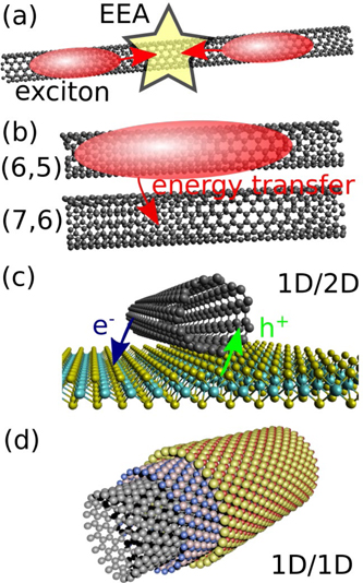
Figure 19. (a) EEA in a CNT in the diffusion-limited regime. (b) Exciton energy transfer proceeding from a larger bandgap (6, 5) CNT to a smaller gap (7, 6) tube. (c) A mixed-dimension vdW heterostructure comprising a CNT bound to a TMD monolayer, creating a 1D/2D heterojunction. (d) A radial vdW heterostructure made from nanotube building blocks, forming 1D/1D heterojunctions.
Download figure:
Standard image High-resolution imageA further ongoing discussion is centred upon the nature of the THz photoconductivity of CNTs [176, 177]. Both normal photoconductivity, where photoexcitation creates mobile charges with a finite conductivity, and unusual negative photoconductivity, where visible light absorption lowers the sample's THz conductivity, have been reported for CNTs [176, 177]. In doped CNTs, photogenerated excitons can interact with equilibrium extrinsic charges and form trions, lowering the free carrier density and enhancing their mass. It is also important to correctly include the equilibrium THz conductivity in the analysis of experimental data [177]. THz radiation has also been used to probe the internal transitions of dark excitons in isolated CNTs [178], in a way not possible using PL.
While isolated CNTs (often in solution) are valuable for fundamental spectroscopic studies of the intrinsic properties of CNTs, real-world devices often require thin-film materials that can be electrically contacted. In this geometry the vdW force creates CNT bundles, and charge or energy can readily transfer between CNTs within the same bundle. Ultrafast coherent spectroscopy uses a sequence of three pulses at different relative delays to create a coherent output beam via four-wave-mixing [179]. Benefits include the ability to distinguish coherent and incoherent relaxation processes, and identifying coupling between resonances [179]. Ultrafast coherent spectroscopy has thus provided a powerful method to examine tube–tube energy transfer rates (figure 19(b)) for semiconducting tubes, showing that excitons migrate to the larger diameter, lower bandgap CNTs within a few ps [180]. Importantly, the mechanism involved was found to not depend on the spectral overlap of the initial and final CNT involved, ruling out the Förster energy transfer model traditionally applied to molecules with large dipole moments. A current challenge is therefore to extend experimental and theoretical investigations in this area to better distinguish between the alternative non-Förster energy transfer mechanisms suggested [180]. Complementary experiments on energy and charge transfer rates should also be performed on heterostructures containing metallic/semiconducting or metallic/metallic CNT junctions.
In addition to composites containing different CNTs, striking new functionalities are predicted by combining 1D CNTs with 2D materials (figure 19(c)), such as TMDCs, in mixed-dimensional 1D/2D vdW heterostructures [181]. TMDCs also exhibit strong excitonic effects, which are not desirable in device applications based on photocurrent (e.g. solar cells; photocatalysis), and excitons often recombine too quickly. CNTs provide an attractive material for 1D/2D heterojunctions, offering rapid charge extraction if energetically favourable. Recent studies using ultrafast TA spectroscopy have shown that electron and hole extraction times in heterojunctions between MoS2 monolayers and (6, 5) CNTs are fast (<1 ps), and that after charge separation, the trions formed in the CNTs are very long lived (730 ns lifetime) [182]. The combination of fast charge extraction plus slow decay is ideal for energy and photochemical reactions, as yields are maximised when electrons persist longer.
CNTs and CNT bundles can be used as the template for growth of radial 1D vdW heterostructures, such as pictured in figure 19(d). These can be regarded as 1D/1D heterojunctions in the quantum limit (small tube diameters), where the electron (or exciton) wavefunction wraps around the nanotube's circumference. Radial 1D vdW heterostructures comprising CNTs wrapped by BN and MoS2 nanotubes combine the attractive excitonic properties of both CNTs and MoS2 [183]. A dynamic change in THz photoconductivity from negative photoconductivity (from the CNTs) to positive photoconductivity (from the MoS2) indicated the good electrical mobility of the MoS2 NTs, and further showed the possibility to combine dissimilar nanomaterials to create composites with a unique ultrafast response [183].
12.3. Advances in science and technology to meet challenges
In order to progress from basic knowledge of ultrafast science into useful technological applications, carbon-based 1D vdW materials must be integrated into functional ultrafast devices. Thin-films of CNTs are already promising in this regard: the strongly non-linear excitonic absorption of CNTs makes them attractive as saturable absorbers for pulsed lasers, with recent work showing the mode-locking regime of fibre lasers can be controlled electrically by changing the saturable absorption of CNT bundles integrated onto an optical fibre [184]. CNTs are also under development as ultrafast sources, either producing electron pulses via photoemission [185] or making pulsed THz radiation from spontaneous exciton ionisation [186].
Controlling and exploiting atomic-scale defects in 1D vdW materials will be important for their future functional use. Such defects in bulk crystals (e.g. the NV− defect in diamond) have been widely explored for nanoscale magnetometry and quantum computing applications, and ultrafast spectroscopy has helped understand how these defects couple electronically and vibrationally to their surroundings by probing the lifetime of coupled vibronic transitions [187] or vibrational relaxation dynamics [188]. However contemporary work has been performed on macroscopic ensembles of defects, in bulk materials: advances in ultrafast techniques are required to study smaller ensembles, with the goal of studying nanomaterials containing isolated atomic-scale defects. Here, techniques similar to ultrafast STM (section 14 by Cocker and Hegmann) that combine atomic spatial resolution and femtosecond temporal resolution may be deployed in the future.
12.4. Concluding remarks
Understanding ultrafast charge and energy transfer processes in these new classes of heterostructures based on CNTs will constitute substantial challenges over the next decade, in order to fully unlock their applications in photonic devices and energy generation. The ultrafast dynamics within each constituent material (e.g. EEA, trapping) needs to be fully understood, and may mask the timescales for transfer between the components (e.g. from a TMDC to a CNT). No single technique can fully explain all the salient photophysical properties and multiple ultrafast spectroscopy methods, covering a wide range of the electromagnetic spectrum and a range of length scales, must be deployed to unpick the complex tangle of ultrafast processes in carbon-based vdW heterostructures.
Acknowledgments
MGB thanks the Russian Government for financial support (Global Education programme).
13. Ultrafast near-field spectroscopy of semiconducting and strongly-correlated nanomaterials
Jessica L Boland
University of Manchester, United Kingdom
13.1. Status
Ultrafast spectroscopy with nanometre spatial resolution is essential for understanding and controlling light–matter interactions at the nanoscale. Conventional far-field ultrafast techniques suffer from poor spatial resolution: the diffraction limit of light restricts radiation to a diameter of λ/2, providing only micron spatial resolution at long wavelengths (150 μm for 1 THz). This spatial resolution is much larger than the dimensions of nanostructures along their confinement directions (1–100 nm), restricting measurements to nanomaterial ensembles and averaging over sample inhomogeneity. It also makes it difficult to optically resolve the transport of carriers and/or excitations (e.g. plasmons) that occurs on sub-µm length scales in real space and time. To overcome this, scanning near-field optical microscopy (SNOM) has been combined with ultrafast techniques to probe both the optoelectronic and vibrational dynamics of semiconductor and strongly-correlated materials with sub-ps temporal and nanoscale spatial resolution.
13.1.1. Aperture-type vs scattering-type
SNOM exploits evanescent fields localised around sub-wavelength structures to locally interact with a sample, overcoming the far-field resolution limit and providing access to nanoscale information. For aperture-type techniques (a-SNOM), the ultrafast laser source is focussed through a sub-wavelength aperture, experiencing sub-diffractional scattering that confines the incident field without any far-field background to a volume set by the aperture size (limited to λ/10 due to waveguide cut-off) [189]. Light transmission also depends strongly on aperture size, reducing by 104 for 100 nm aperture. Careful aperture design is therefore required to achieve the best spatial resolution with sufficient SNR to detect the near-field signal. As the spatial resolution is wavelength-dependent, a-SNOM has become extremely popular for ultrafast near-field pump-probe spectroscopy in the UV–NIR range, where apertures do not suffer from frequency cut-off and high-power sources (e.g. ultrafast fibre-based amplifiers) are readily available. This has led to the first ultrafast study of the coherent nonlinear optical response of a single GaAs QD [190].
In contrast, scattering-type techniques (s-SNOM) utilise a metallic atomic force microscope (AFM) tip as the nanoscale probe, confining ultrafast pulses to a volume defined by the tip radius of curvature. When the tip approaches the sample, it scatters the near-field signal back into the far-field, where it can be detected using conventional far-field techniques [e.g. electro-optic (EO) sampling] [192]. s-SNOM removes the need to fabricate nanoscale apertures and provides a higher wavelength-independent spatial resolution only limited by the tip radius (∼10 nm). However, the large scattered far-field background signal produces unwanted artefacts, making direct extraction of near-field information challenging. To suppress this background, s-SNOM is operated in AFM-tapping mode with the measured signal demodulated at higher harmonic orders of the tip oscillation frequency, where the near-field contribution dominates. Combining s-SNOM with ultrafast spectroscopy has pushed near-field studies out to long wavelengths (MIR–THz) and length scales <50 nm, providing important breakthroughs: starting with the direct observation of ultrafast plasmon phenomena in graphene [192] and the extraction of the time-dependent dielectric function of a single InAs nanowire [193]; and more recently, exciton–polariton formation and propagation in WSe2 [194].
13.1.2. Moving to the THz range
Ultrafast near-field THz time-domain spectroscopy (THz-TDS) holds enormous promise, as the THz range encompasses many low-energy excitations residing in nanoscale quantum systems, including phonons, magnons, and energy gaps in high-TC superconductors. Near-field THz-TDS via a-SNOM consistently provides µm-spatial resolution—an ideal range for spatio-temporal mapping of THz SPs in graphene and sub-surface modes in strongly coupled resonators. To push towards nm-spatial resolution, current efforts are focussed on coupling ultrafast THz pulses to s-SNOM. However, the low scattered signal and lack of high-power THz sources available pose technical difficulties. To overcome this, approaches have included THz emission microscopy, phase-resolved near-field detection via self-mixing in a THz quantum cascade laser (THz-QCL), and detection of THz-induced near-field photocurrent [195]. Yet, in the past year, ultrafast near-field optical-pump/THz-probe spectroscopy has been demonstrated using photoconductive antennas (PCAs), allowing the photoinduced dynamics of graphene/InAs heterostructures to be explored [196].
13.2. Current and future challenges
13.2.1. Cryogenic operation
Nanoscale investigation of several exciting solid-state phenomena, including phase transitions in perovskites and multiferroics, requires cryogenic operation. In particular, low temperatures are essential for THz frequencies, where THz resonances are often screened at room temperature. a-SNOM operating at liquid helium temperature is already well established, yet restricted to visible and NIR wavelengths. Cryogenic s-SNOM faces more technical challenges associated with conventional tapping-mode AFM in ultrahigh-vacuum (UHV) environments. Several independent piezoelectric positioners with large scanning ranges are required; and drift due to thermal expansion/contraction of the tip and sample supports must be considered. Optical access to the tip also requires high-NA collection optics and good radiation shielding to account for thermal loss due to optical components. Cryo-s-SNOM was first demonstrated in a home-built system to observe the insulator–metal transition of V2O3 at ∼150 K [197]. Since then, operation temperature has lowered significantly, enabling direct imaging of plasmon–polariton propagation at 60 K in graphene [198]. However, cryogenic ultrafast s-SNOM remains in its infancy. Commercial cryo-s-SNOM (∼10 K) systems (attocube, neaspec) are now readily available, easing technical challenges of UHV operation. Yet, improvements in sensitivity and artefact-free near-field detection will also be essential to probe nanoscale dynamics at low temperature on ultrafast timescales.
13.2.2. High magnetic fields
Ultrafast s-SNOM in strong magnetic fields is another exciting development that would allow direct imaging of magnetic domains and spin dynamics on nm-length scales. While one system reaching magnetic fields up to 7 T has been presented [197], no experimental studies have yet been reported. As commercial cryo-s-SNOM systems with integrated superconducting magnets become available and technical challenges are addressed, ultrafast near-field magneto-spectroscopy could become widespread, opening up a new research area for investigating low-dimensional materials.
13.2.3. Increased sensitivity
To ensure adequate SNR for near-field detection, high-power sources are routinely used with high-repetition-rate ultrafast lasers. A high repetition-rate guarantees high average incident power (and thereby high SNR), yet at the cost of small pulse energy and heating at the tip/aperture. It also places a limit on available light sources—a specific problem for ultrafast s-SNOM in the THz range, where typical sources (e.g. PCAs) have output powers of <50 μW. Field-resolved detection via EO sampling is therefore essential to achieve sufficient SNR to detect the near-field. While further development of ultrafast high-power THz sources will improve sensitivity, an alternative approach is to combine SNOM with low-repetition-rate (∼kHz) ultrafast lasers, reducing accumulative heating and broadening the range of sources available. For tapping-mode s-SNOM, the repetition rate is limited by the Nyquist–Shannon sampling theorem. However, phase domain sampling removes this theoretical limit, allowing s-SNOM at repetition rates below the tip-tapping frequency (Ω) [199]. This allows ultrafast laser sources with high pulse energy to be coupled to the tip, simultaneously increasing both sensitivity and local field enhancement. Further gains, including increased polarisation control and/or spatial resolution, could also be achieved through structural tip engineering. Such advances combined with field-resolved detection would not only provide improved sensitivity to spatio-temporally map propagating plasmonic wavepackets; but also sufficiently large field strengths at the tip apex to induce and probe nonlinear dynamics on the nanoscale (figure 20).
Figure 20. Top left: schematic diagram of a-SNOM technique, where the far-field incident light is directed through a sub-wavelength aperture, producing an evanescent near-field at the sample. The near-field light can be detected either in transmission or reflection. Bottom left: schematic diagram of s-SNOM technique, where the incident far-field is coupled to an AFM tip, producing an evanescent near-field at the tip apex. The desired near-field signal and large far-field background signal is scattered back from the tip and detected using conventional far-field techniques. Right: graphical summary of possible applications of s-SNOM for different incident energies and spatial resolution. The shaded areas depict the accessible spatial resolution for each frequency range for ultrafast STM (red), s-SNOM (blue) and a-SNOM (yellow) respectively.
Download figure:
Standard image High-resolution image13.2.4. Artefact-free detection
A key challenge facing ultrafast s-SNOM is accurate near-field extraction, as the measured signal contains both the desired near-field information and a large scattered far-field background. While operating s-SNOM in tapping-mode largely suppresses this background, an appropriate detection technique must be chosen. For ultrafast s-SNOM, field-resolved detection has been widely used to extract both the amplitude and absolute phase of the scattered near-field waveform. Recently, intensity-based detection techniques have been extended for use with ultrafast pulses [200]. By combining pseudoheterodyne detection with two digital boxcars, the background-free demodulated signal can be collected just before and after a pump pulse is applied. Providing the time delay between the probe pulses (i.e. between off/on) is long enough for the sample to relax back to steady-state, the difference ( ) will yield both the amplitude and relative phase of the photoinduced near-field signal. However, it is important to note that artefacts can still remain for both detection techniques. Appropriate harmonic orders must therefore be chosen to reduce the background signal enough that the near-field response dominates. At NIR, MIR, and THz wavelengths, the 3Ω, 2Ω, and 1Ω respectively are sufficient. However, for UV and visible, very high harmonic orders (>4Ω) and small tapping amplitudes are essential. To address this, novel approaches are required that remove the need for tapping-mode operation. For example, plasmonic-nanofocussed four-wave-mixing on a grating-coupled conical tip has recently been used to probe localized SP hotspots in gold on <10 fs timescales [201]. Such techniques could pave the way for artefact-free detection in the UV, visible range and beyond.
13.2.5. Increased spatial resolution
Ultrafast near-field spectroscopy is constantly moving to smaller length scales. While s-SNOM consistently achieves ∼10 nm spatial resolution, it is theoretically limited only by the tip radius of curvature. As described in section 14 by Cocker and Hegmann, ∼2 nm spatial resolution has been achieved via THz-STM to image the ultrafast dynamics of a single molecule. As THz-STM and cryogenic s-SNOM effectively utilise the same hardware, integrating the two techniques could push ultrafast s-SNOM down to molecular/atomic length scales. However, this will only be achieved alongside advances in cryogenic operation and sensitivity.
13.3. Concluding remarks
Ultrafast near-field spectroscopy has already become a powerful tool for non-destructive optoelectronic characterisation of semiconducting and strongly-correlated materials. Its versatility across a broad frequency range allows for integration with several techniques (e.g. nano-XRD, SERS), opening up a large parameter space for nanoscale investigation. The next step is to push the technique to the extreme: longer wavelengths, atomic/molecular length scales, low temperatures < 10 K and strong magnetic fields.
Acknowledgments
J L Boland would like to acknowledge and thank the EPSRC (EP/S037438/1, EP/T01914X/1) and Leverhulme Trust (Philip Leverhulme Prize) for research funding and support.
14. Ultrafast lightwave-driven scanning tunnelling microscopy
Tyler L Cocker1 and Frank A Hegmann2
1Michigan State University, United States of America
2University of Alberta, Canada
14.1. Status
The promise of ultrafast STM has motivated three decades of development effort, as the vision of dynamic electron densities filmed in atomic resolution movies continues to inspire. This scientific goal is finally within reach. Many of the technical challenges that long limited progress have now been solved through the concept of lightwave-driven STM (LWD-STM) [202–204, 206, 208, 213, 214], which introduces femtosecond temporal resolution without sacrificing the strengths of steady-state STM, such as atomic spatial resolution and spectroscopic sensitivity.
LWD-STM builds on progress from complementary approaches to time-resolved STM, from all-electronic schemes [207] to techniques based on photoexciting the junction with free free-space optical pulses [205, 211]. Perhaps the most direct precursor of LWD-STM is junction-mixing STM [209], a technique in which voltage pulses generated by photoswitches are launched down a transmission line on the sample. The voltage pulses subsequently exploit the nonlinearity of the tunnel junction's current–voltage characteristic to overcome the relatively low duty cycle and produce a measurable ultrafast signal.
The nonlinearity of the current–voltage characteristic is similarly important in LWD-STM, but the voltage pulses are replaced by free-space, carrier-envelope-phase-stable light pulses focussed directly onto the STM tip, removing the need for a transmission line. The tip acts as a long-wire antenna, enhancing the field of the pulse at the tip apex, where its maximum reaches the strong-field regime. In the strong-field regime, an oscillating electromagnetic wave can be treated as a quasi-static modulation of the potential energy landscape, so the pulse behaves as an ultrafast bias voltage transient that acts on the instantaneous current–voltage characteristic, generating an ultrafast current pulse. The STM electronics cannot resolve the oscillatory features of this current pulse because the oscillation rate far exceeds the detection bandwidth, but the electronics can measure its rectified component. The current pulse contains a rectified component, even though the temporal integral of the incident pulse is zero, thanks to the nonlinearity of the current–voltage characteristic. Such nonlinearities are present in almost all STM tunnel junctions, since the local density of states of the sample varies as a function of energy (i.e. STM bias voltage). Because the rectified component of the current pulse is ultimately measured as an average over many pulses to increase sensitivity, the phase stability of the incident pulse is essential for LWD-STM. The shape of the electromagnetic waveform at the tip apex is also a key consideration, and should ideally be only a single oscillation cycle long.
Ultrafast LWD-STM was first demonstrated using pulses in the terahertz (THz) spectral range—an implementation called THz-STM—with proof-of-principle NIR pump/THz-STM probe experiments in ambient conditions [202]. The field of THz-STM has developed rapidly since then, with ultrahigh vacuum, cryogenic operation becoming standard [203, 206]. Atomic spatial resolution with simultaneous sub-picosecond temporal resolution has been shown for silicon surfaces in a fully THz-driven mode, where no DC bias is present and the STM feedback loop responds only to THz-induced tunnel currents [206]. These tunnel currents can reach extreme scales due to their ultrafast duration, opening up a new direction for exploration. Meanwhile, state-selective tunnelling in the regime of one electron per pulse has been achieved for THz-STM of single molecules [203]. It has been shown that the peak field of a THz pulse can remove a single electron from a single molecular orbital within a time window faster than an oscillation cycle of the THz wave. This has allowed the electron density of a single molecular orbital to be captured in ∼100 fs snapshot images with sub-angstrom spatial resolution. THz pump/THz probe experiments have further revealed the picosecond motion of a single molecule following the lightwave-driven tunnelling process. Recently, the concept of LWD-STM has also been extended to the sub-femtosecond timescale using phase-stable NIR pulses [204], following the demonstration of NIR field-emission control in an optical antenna geometry [210]. We discuss the relative merits of different frequency ranges for LWD-STM (illustrated in figure 21(a)) in the next section.

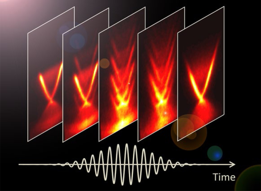
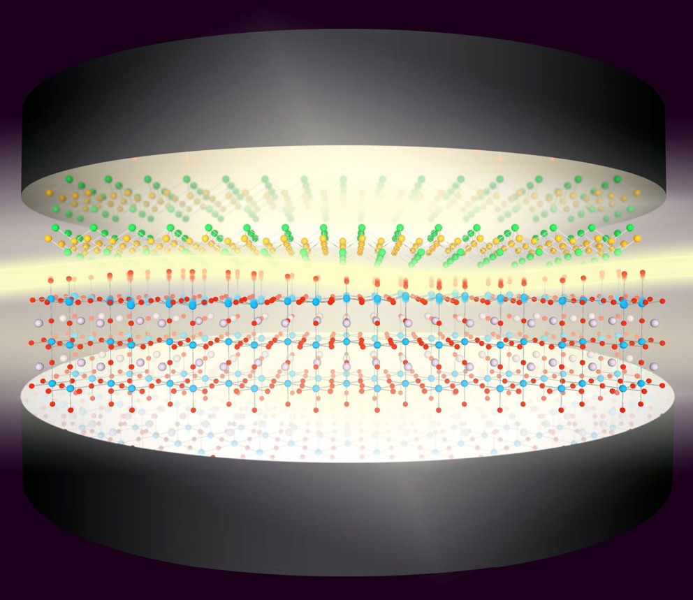
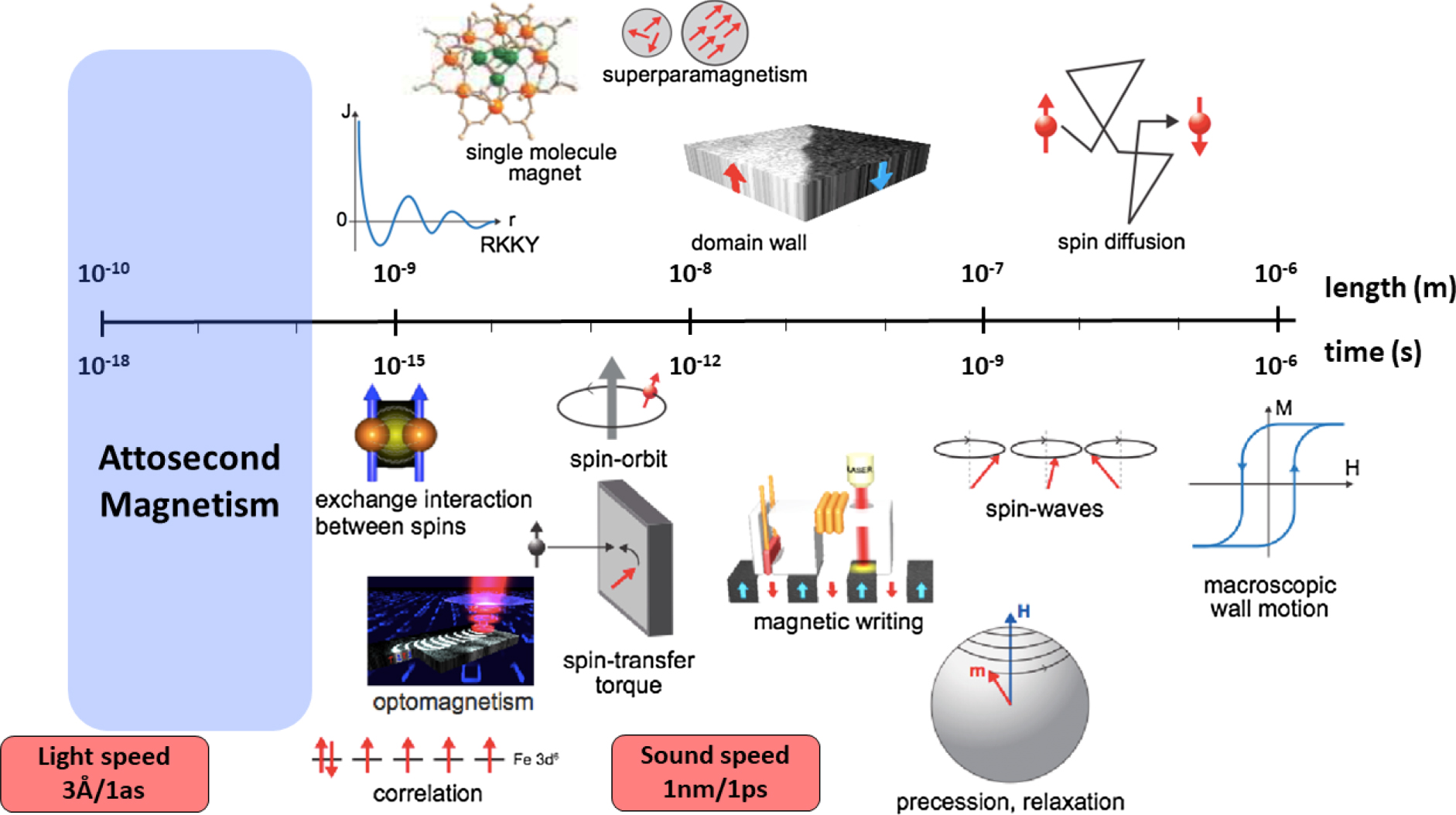
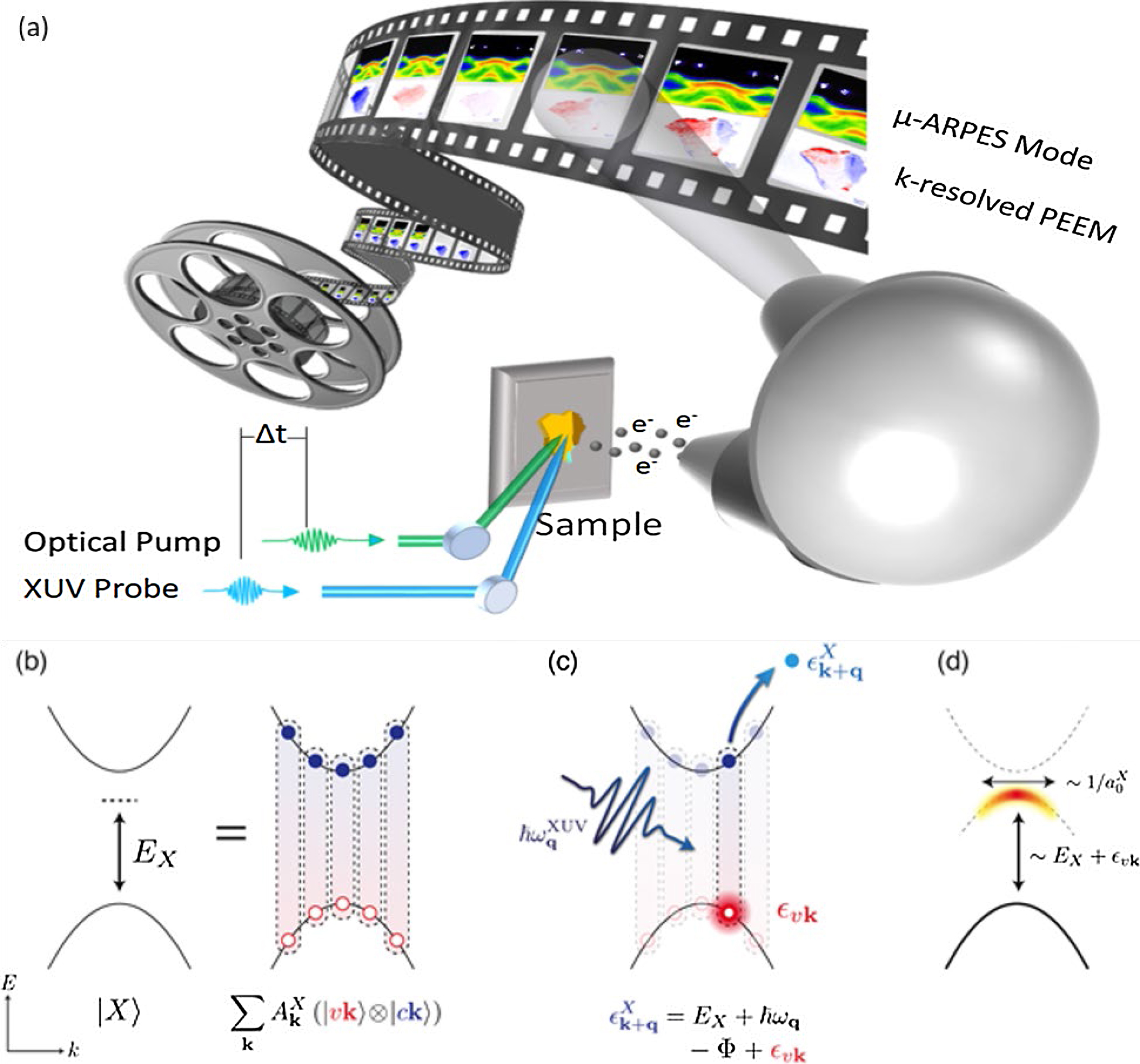
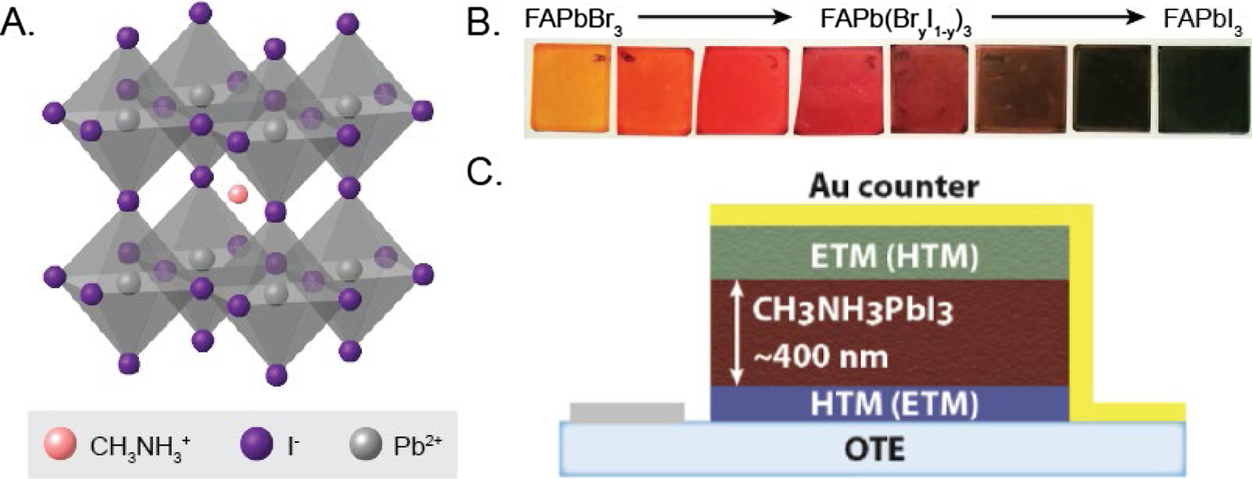
Figure 21. LWD-STM at different frequencies. (a) Experimental scheme: an ultrafast, phase-stable, single-cycle pulse in the terahertz (THz), mid-infrared (MIR) or near-infrared (NIR) spectral range is focussed onto the tip of a scanning tunnelling microscope, where its field, E(t), coherently controls the current across the tunnel junction. The nonlinearity of the tunnel junction leads to an asymmetric current pulse, i(t), with a rectified component that can be detected by time-integrating electronics. The duration of the current pulse for unipolar tunnelling is less than half an oscillation cycle of the probe, defining the time resolution. The relative oscillation frequencies are not to scale. (b) The lightwave-driven tunnelling concept holds in the strong-field regime of optical nonlinearity, defined here as γ < 1, where γ is the Keldysh parameter. Solid lines show voltages for which γ = 1 for different scanning tunnelling microscope tip heights. Above the work function of the sample (εI = 5 eV here, grey dashed line) the tunnel apparent barrier width becomes voltage dependent, corresponding to the field-emission regime (grey shaded region). The frequencies of the pulses in (a) are shown as vertical dashed lines (red: THz, 1 THz; green: MIR, 30 THz; blue: NIR, 300 THz). We note that for a constant input field the voltage applied across the junction is constant, i.e. it does not change with d [206, 208], and emphasize that (b) is a conceptual map of the relevant LWD-STM regimes, not field enhancement.
Download figure:
Standard image High-resolution image
14.2. Current and future challenges
We focus our discussion on the steps needed to fulfil the scientific promise of LWD-STM, with particular emphasis placed on potential impediments to imaging transient electron densities on the atomic scale. We believe that LWD-STS will be an essential complementary tool in the future for understanding the phenomena observed in such snapshot images. Here, we define LWD-STS as an analogue of steady-state STS, i.e. as an experimental means to extract the time-dependent differential conductivity as a function of voltage. We propose that the ultrafast evolution of the differential conductivity can be directly related to the transient occupation of the local density of states. Developing a practical and comprehensive approach to LWD-STS is therefore considered to be a high priority.
So far, THz-STM signals have typically been modelled by assuming a reasonable current–voltage characteristic and simulating the lightwave-driven tunnelling process. This can be done as a function of peak field strength [202, 203, 206, 214], tip height [206], or time between two pulses [202, 203, 206] to constrain the free parameters. Alternatively, for samples that respond to NIR excitation much faster than the THz oscillation cycle, it has been suggested that the rectified current vs THz peak field traces out the transient current–voltage characteristic [213]. However, this approach averages over the lifetime of the excitation, precluding time-dependent THz-STS. A challenge for the future is to develop a method to directly extract time-dependent differential conductivities from arbitrary lightwave-driven signals.
An additional challenge for the prospect of ultrafast THz-STS is that coupling THz pulses to the STM tip can substantially affect the temporal shape of the THz waveform. We anticipate that knowing the precise field profile will be important for future THz-STS inversion algorithms. A promising development to this end has been the demonstration of THz streaking of electrons photoemitted from a sharp metal tip [212] and the subsequent adaptation of this approach to the STM geometry [208, 213], which provides a convenient way to sample the THz waveform at the tip apex. One potential challenge we foresee for this approach is that when the sample contains a strong resonance within the bandwidth of the probe pulse the field in the junction will feature a free induction decay [193] that is not present when the tip is retracted from the surface (or in close proximity to a test sample). In such a case, an in situ alternative to photoemission sampling may be necessary, e.g. scattering-type scanning near-field THz microscopy (see section 13 by Jessica L Boland). Here, we note that it is important to distinguish between the spectral content of the in-coupled pulse, i.e. the amplitude of its Fourier transform, and LWD-STS, through which the intrinsic physics of the tunnel junction is related to the field of the driving pulse.
The spectral content of the input pulse is also a key parameter for its field enhancement at the tip apex. Whereas the field enhancement at THz frequencies reaches 105 to 106 in THz-STM [202, 203, 206, 208, 213, 214], this enhancement is inversely proportional to frequency due to capacitive effects. Tip heating is also more prominent at higher frequencies, as has been observed recently in LWD-STM experiments at NIR frequencies [204]. Nevertheless, the fastest time resolution in LWD-STM is achieved with the highest driving frequencies. Therefore, with this motivation, we outline some of the key considerations and challenges in designing future ultrafast sources for LWD-STM.
To fully realize the potential time resolution for a given frequency, the pulse should be only a single oscillation cycle long. Furthermore, the pulses should be phase-stable and of sufficient field strength to drive tunnelling, while the laser repetition rate should be high enough to produce a measurable signal. The duty cycle of the lightwave-driven current and its interplay with tip height is another key consideration. For typical THz-STM parameters (100 fs current pulses, 1 MHz repetition rate) the duty cycle is 10−7. To account for this and produce a measurable average current, the tunnel rate must be increased for THz-STM experiments. One way to do this while maintaining STS function is by operating with a tip height that is closer to the sample than for steady-state STM operation. For the same peak voltage at higher probe frequencies, and hence lower duty cycles, the tip must be moved yet closer to the sample, which is not always stable, or the repetition rate must be increased, though this conversely leads to larger heating effects [204]. Most importantly, the compatibility of a given frequency and peak field strength with the concept of lightwave-driven tunnelling should be considered. The Keldysh parameter, γ, distinguishes the strong-field regime (γ < 1), in which lightwave-driven tunnelling occurs, from the multi-photon regime (γ > 1) of optical nonlinearity. It is given by  , where ω is the angular frequency of the driving field, me is the electron effective mass, εI is the ionization energy or barrier height, e is the charge of the electron, and E is the driving field strength. The Keldysh parameter can also be written as γ = ω/ωt, where ωt is the tunnelling rate through the barrier. The minimum voltage V that can be applied across a tunnel junction of width d within the strong-field regime is
  . Figure 21(b) shows the result of this calculation as a function of frequency f = ω/2π and oscillation period T = 1/f for a typical material work function of ɛI = 5 eV. For voltages above ɛI/e the system enters the field emission regime, where the apparent gap width depends on voltage and the spatial resolution degrades, at least for steady-state STM. Reducing the gap distance improves the situation, allowing lower voltages to be used for lightwave-driven tunnelling at a particular frequency. However, there is a clear trade-off between time resolution (10% to 50% of one oscillation period for a single-cycle pulse, depending on the nonlinearity of the current–voltage characteristic) and the voltage range over which the concept of lightwave-driven tunnelling holds. For example, NIR and optical frequencies are predicted to reach the strong field regime only for voltages above the work function. In general, figure 21(b) serves as a guide for selecting an appropriate probe frequency for a particular LWD-STM experiment.
A final challenge is to develop versatile schemes for selecting sample excitations for pump-probe measurements. One approach is to use multiple frequencies, such as a non-phase-stable optical or NIR pump that excites the sample globally and a THz-STM probe that images the local response [202, 213]. In the future, time-resolved THz-STS will further reveal transient changes to the current–voltage characteristic induced by the pump. Another approach is to employ both a coherent pump and probe, for example in a local, lightwave-driven excitation [203] or in a cross-polarized geometry to independently couple to the sample [204], though care must be taken to account for interference and nonlinear heating. A key to widening the reach of LWD-STM will be to use these and other geometries to target specific phenomena of interest with high efficiency. For oscillatory phenomena, the initial phase of the oscillation needs to be locked to the excitation process in order for its effect to be imprinted on the average lightwave-driven current [203]. Another potential strategy is to spatially separate a local excitation from the lightwave-driven probe, for example by using a multi-probe STM geometry. In general, combining LWD-STM with other advanced scanning probe techniques promises to introduce yet new possibilities, both for further technical advances and for a richer understanding of the dynamics of the tunnel junction.
Looking forward, new challenges, both technical and conceptual, may arise as the scientific scope of LWD-STM expands. Nevertheless, tackling these challenges will be well worth the effort, as LWD-STM affords a unique view of the nanoworld. Unlike diffraction-based probes, it images directly in real-space, and remains the only ultrafast microscopy technique for which simultaneous atomic spatial resolution and sub-picosecond temporal resolution has been demonstrated. It provides exclusive access to dynamics in a number of systems, including the ultrafast motion of single molecules and, in principle, wavefunction dynamics. The prospects for future LWD-STM studies are diverse, ranging from atomically-resolved dynamics in quantum materials to quantum statistics in the regime of few quasiparticles. Ultimately, we envision its influence reaching past fundamental materials research to impact incipient technology, such as next-generation solar energy conversion and quantum computing.
14.3. Concluding remarks
With the advent and rapid development of LWD-STM, especially at THz frequencies, ultrafast STM has now progressed beyond the demonstration phase. A number of steps still remain to make the technique practical and generally applicable, but it can now be employed for scientific exploration. We forecast an exciting time for the field over the next five years, as the number of groups working in ultrafast STM expands. We note that even since the submission of this roadmap a number of new LWD-STM papers have been published [215–219] that we unfortunately do not have space to feature here. Movies of transient electron densities resolved in energy, space, and time with femtosecond temporal resolution and atomic spatial resolution may even be widespread in the near future.
Acknowledgments
The authors thank V Jelic, S E Ammerman, and R Huber for valuable discussions. TLC gratefully acknowledges support from the Cowen Family Endowment and the Office of Naval Research (Grant No. N00014-19-1-2051). FAH gratefully acknowledges support from the Natural Sciences and Engineering Research Council of Canada (NSERC), the Canada Foundation for Innovation (CFI), and the Alberta Innovates Technology Futures (AITF) Strategic Chairs Programme.
Data availability statement
The data that support the findings of this study are available upon reasonable request from the authors.