
Abstract
The spatio-temporal dynamics of electrons moving in a 2D plane is challenging to detect when the required resolution shrinks simultaneously to nanometer length and subpicosecond time scale. We propose a detection scheme relying on phonon-induced carrier capture from 2D unbound states into the bound states of an embedded quantum dot. This capture process happens locally and here we explore if this locality is sufficient to use the carrier capture process as detection of the ultrafast diffraction of electrons from an obstacle in the 2D plane. As an example we consider an electronic wave packet traveling in a semiconducting monolayer of the transition metal dichalcogenide MoSe2, and we study the scattering-induced dynamics using a single particle Lindblad approach. Our results offer a new way to high resolution detection of the spatio-temporal carrier dynamics.
Export citation and abstract BibTeX RIS

Original content from this work may be used under the terms of the Creative Commons Attribution 3.0 licence. Any further distribution of this work must maintain attribution to the author(s) and the title of the work, journal citation and DOI.
1. Introduction
Detecting the spatio-temporal dynamics of generic (quasi-)particles [1–11] is challenging when a subpicosecond temporal scale has to be combined with a nanometer spatial resolution [4, 8]. Nevertheless it is of high interest to unravel the spatio-temporal carrier dynamics to use it, e.g. in quantum information protocols, and several studies have investigated how small wave packets evolve or can be controlled [12–16].
In this paper we propose a mechanism to detect and reveal the spatio-temporal dynamics of an electronic wave packet moving in a semiconducting two-dimensional (2D) system. The detection mechanism relies on the phonon-induced carrier capture [16–29] from the delocalized states in the 2D host material into the bound states of a quasi-zero dimensional quantum dot (QD) embedded in this material. The captured carriers can then recombine on a longer time scale resulting in an optical signal spectrally well separated from the host material's optical signals, providing information on the time-integrated carrier capture into the QD. Using ultrafast pump-probe spectroscopy on a single QD [30, 31], time-resolved information on the QD population, and thus on the capture process, can also be obtained [27]. The crucial aspect for the detection is that the carrier capture happens locally [16, 25–29], i.e. only when the electronic density is close to the QD it can be captured. Here we analyze the question, whether this locality is pronounced enough to describe where the electronic wave packet was distributed. In other words, we examine, if the phonon-induced carrier capture can be used to spatially resolve efficiently the ultrafast dynamics of the electronic density.
As a testbed, we will consider the diffraction of an electronic wave packet moving in a monolayer of a transition metal dichalcogenide (TMDC) at an obstacle. TMDCs represent a class of 2D semiconducting materials which has recently attracted lots of attention [32–38], mostly due to their excitonic properties, although a mixture of bound and unbound electron–hole pairs could be present [39, 40]. In these materials QDs can be created efficiently, e.g. by applying a tensile strain [41–48], resulting in clearly resolved optical signals. Alternatively, a localized attractive potential for a single type of carriers—electrons or holes—can be achieved by applying a strongly localized gate voltage, e.g. by means of a tip of a scanning tunneling microscope. Such tip-induced QDs have already been realized in graphene [49], and tip-induced band-bending effects in  monolayers of few tens of meV have been estimated [50]. While QDs result from an attractive localized potential in the monolayer, an obstacle is formed by a repulsive localized potential. For tip-induced potentials this could be reached by reversing the voltage (see, e.g. [51]). Also, a strongly localized compressive strain, which increases the band gap of TMDCs [52, 53], would result in an obstacle for the carriers. When an electronic density travels inside the TMDC monolayer and gets diffracted at such an obstacle, the spatial dynamics can be theoretically calculated exactly in well specified points. We compare this exact quantity with the predictions provided by the proposed carrier-capture detection scheme, which can be experimentally realized. This will give insight in the efficiency of the proposed scheme.
2. Capture-free dynamics
To be specific, we will consider an electronic wave packet moving in a monolayer of MoSe2, which gets diffracted by an obstacle. The resulting spatial distribution evolves in fringes which, in view of their amplitude and separation, may be challenging to address.
The initial state is assumed to be a pure state with wave function ![$ \newcommand{\im}{{\rm Im}} \newcommand{\e}{{\rm e}} \psi(\mathbf{r})\propto \sum_{k_x} {\rm exp} \left[-\left(\epsilon_{k_x} - E_0 \right){}^2/(2\Delta_E^2)\right] {\rm exp}\left[\imath k_x (x-x_{{\rm WP}})\right]$](https://content.cld.iop.org/journals/0953-8984/31/28/28LT01/revision2/cmab17a8ieqn002.gif) . The energy has a Gaussian distribution in x-direction with
. The energy has a Gaussian distribution in x-direction with  being the energy of the electronic eigenstate in the bare monolayer labeled by the 2D wave vector
  ,
,  is the energy width and E0 the excess energy. The energies
  for TMDC monolayers are essentially parabolic close to the band gap [28]. In the y -direction the wave packet is homogeneous. Taking E0 = 26.8 meV and
  meV, this results in a spatial charge density
  (with
(with  being the 2D space vector) behaving as a wavefront with initial FWHM of about 40 nm in x-direction. The initial position of the wave packet is given by
  nm and we assume the wave packet moves to the right. A sketch of the initial wave packet is seen in figure 1(a) on the left side. Such a wave packet could be considered as the far field of a localized optical excitation [28] induced by, e.g. near-field or plasmonic excitation [30, 54–59] with ultra-fast nano-optics techniques [60].
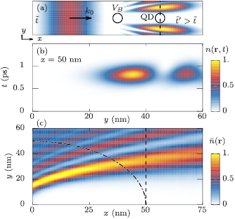
Figure 1. (a) Sketch of the set-up: a wave packet initialized at  (left side) impinges on an obstacle
  resulting in spatial fringes behind the barrier at
  (right side). The electronic density might then be detected by a QD. (b) Temporal evolution of the electronic density
  at x = 50 nm. (c) Time integrated density
  . The dashed and dashed-dotted lines indicate the QD positions probed in figures 2(a) and (b), respectively (note the different scales of the x-and y -axes).
Download figure:
Standard image High-resolution imageAlong the motion of the wave packet we consider an obstacle resulting in a non-trivial spatio-temporal distribution. The obstacle is modeled by a potential barrier  located at the origin. We take
  meV as strength of the barrier and
  nm as its size parameter. After hitting the barrier, the wave packet diffraction leads to fringes with different magnitude and separations as displayed at the right side of figure 1(a). These fringes are on a nanometer scale and we want to explore if our approach is appropriate to resolve them.
In order to understand the timescales, in figure 1(b) we show the temporal evolution of the spatial charge density  along a vertical line at x = 50 nm. Note that the electronic density is normalized to its maximal value. We find that the charge is different from zero only in a small time window centered around a time
  fs and with a width
  of about 300 fs. The time
  quantifies how long the wave packet stays at a given point
  , i.e. the duration of the spatio-temporal dynamics we want to study. Its value indicates that this happens on a (strong) sub-picosecond timescale.
Although the spatio-temporal dynamics takes place on an ultrafast timescale, its memory is included in the time-integrated density  defined as
where we integrate up to a time T being much larger than  . The time-integrated density can be interpreted as the amount of charge which has crossed point
  . We show
  in figure 1(c). We find that the time-integrated density
  displays the non-trivial spatial behavior of the fringes in agreement with typical wave packet dynamics known, e.g. from light waves.
3. Detection via carrier capture
Now we want to explore if the carrier capture into a QD is able to resolve such nanometer-scale diffraction patterns. For this purpose, we introduce a QD described by the confinement potential
describing a QD centered at  with depth
  meV and size parameter
  nm. Such a QD has a single bound state with energy
  meV independently of
  (when the latter is big enough to avoid overlapping with the barrier, as it is the case here). The wave function of this bound state has a full width at half maximum (FWHM) of approximately
  nm and is in good agreement with the wave function of a cylindrical potential well with a diameter of about
  nm. This state can be populated by capturing carriers from the 2D states via interaction with phonons [16, 26, 28]. In the MoSe2 system at low temperature, the capture of conduction-band electrons takes place mostly via the emission of longitudinal optical (LO) phonons [28] with energy
  . In view of the dynamics shown in figure 1, the QD will be crossed by a different amount of charge depending on its position
  . To study the detection capability of the QD, we will compare the time-integrated density
  with the charge trapped in the QD at position
  after the carrier capture. This is given by the quantity
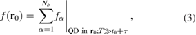
with Nb being in general the number of bound states of the QD (for our QD we have Nb = 1) and  being the population of bound state
  at time T after the wave packet has crossed the QD area. In previous works [26, 28] we have shown that the carrier capture shows an interesting time evolution and the capture takes place only in a finite time-window. Therefore, the final captured density
  is a well defined quantity for every T after this time-window. Thus, even if the readout of the occupation occurs in a time-integrated way, the signal provides information on the dynamics of the wave packet during a short time interval when it is in the region of the QD.
To describe the spatio-temporal carrier dynamics including the interaction with phonons, we use a recently introduced Lindblad single-particle approach within the density matrix formalism [26, 28]. It has been shown that this is a Markovian and trace-preserving [15, 61–64] description of carrier capture. The method is able to catch the locality of the scattering, while remaining computationally lighter than, e.g. full quantum kinetic equations [16, 26]. Details of the method can be found in [26, 28]. The resulting equations of motion for the density matrix elements are numerically integrated by standard finite time-difference techniques.
Figure 2(a) shows the captured density  as function of the QD center at x0 = 50 nm and varying y 0 (see vertical dashed line in figure 1(c)). For comparison we also show the time-integrated electron density
  at x = x0 = 50 nm and y = y 0. Both functions have been normalized to their center of the oscillations defined by the average between the second maximum and minimum. The agreement between these two curves is very good with
  being able to predict the locations of all the fringes displayed by
  . A major difference is the amplitude of the spatial oscillations, which in the capture-induced results of
  are smaller than in the exact case of
  . This deviation originates mostly from the character of the two quantities: while
  is defined at every single point
  , the bound state of the QD has a finite extension, therefore monitoring the density over an extended area. In order to show the contribution of the finite size of the receiving bound state, we consider the spatially averaged density
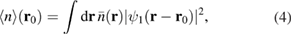
i.e. we coarse grain  by the squared modulus of the receiving bound-state wave function
  . The resulting spatially averaged density
  is shown alongside
  and
and  in figure 2(a). Note that
  is normalized by the same factor as
  . The oscillations of
  now have a reduced amplitude very similar to the one of
  , thus confirming that it is the size of the receiving state which mostly rules the magnitude of the signal provided by the capture-induced experiment. Larger QDs would therefore result in a loss of spatial resolution such that fringes of higher order become less visible. We nevertheless expect that especially the first fringe would still be well separated from the rest of the signal.

Figure 2. Captured electron density  (solid line), time-integrated electronic density
  (dashed line) and averaged electronic density
  for (a) fixed distance x0 = 50 nm and (b) fixed radial distance
  with r0 = 50 nm.
Download figure:
Standard image High-resolution image
To experimentally realize such a set-up this would require movable QDs, which could in principle be created, e.g. by charged tips exploiting the so-called tip-induced band bending [65–67]. Such tip-induced QDs have been created for several years [68–70], resulting in the creation of zero-dimensional confinement potentials few tens of nanometers wide and few tens of meV deep [70], resulting in a deepest bound state with FWHM of about 10 nm, i.e. not far from the FWHM of about 7 nm of the bound state  here considered. We therefore expect that the reported spatial resolution can be achieved experimentally. Although mostly studied through electrical scanning-tunneling spectroscopy measurements, these tip-induced QDs could also be studied optically by putting a proper material under the studied surface [71, 72].
Another option to change the geometrical set-up is to keep the distance between the barrier and the QD fixed and rotate the sample by an angle  around the barrier w.r.t. the incoming wave packet. In such a configuration the shape of the wave packet and the positioning of barrier and QD stay fixed. The corresponding results then lie on a circle with
  and r0 is the fixed distance between barrier and QD (see dashed-dotted line in figure 1(c)). The captured density
  in comparison to the exact results
  and the averaged density
  for the rotation set-up are shown in figure 2(b). At larger angles the captured electron density
  is not able to efficiently address the location of the fringes anymore, because their amplitude and separation (see figure 1(c)) become too small to overcome the previously-described weakening of the amplitude. Nevertheless, as far as one considers bigger peaks, also in the case of figure 2(b) the matching is high, showing that our detection scheme can be performed also without movable QDs.
4. Conclusions
In conclusion, we have proposed a detection method to resolve the nanometer scale electron dynamics in a 2D system. For this purpose we have exploited the phonon-induced carrier capture into the bound states of a QD and shown the efficiency of the relation between exact and captured dynamics. In view of the developments of experimental techniques able to create movable QDs, we believe that the results reported here pave the way to an efficient detection of the spatio-temporal dynamics of low-energy carriers in 2D materials.
Acknowledgments
FL and DER acknowledge financial support from the Deutsche Forschungsgemeinschaft via the Project No. RE4183/2-1.