
Abstract
Hexagonal boron nitride (hBN) is a wide gap 2D layered material with good insulating properties. Intrinsic point defects in hBN play an important role in its applications as a dielectric in 2D electronic devices. However, the electronic properties of these defects are still poorly understood. We have calculated the structure and properties of a wide range of intrinsic point defects in the bulk of hBN using hybrid density functional theory (DFT). These include vacancies and interstitial states of B and N as well as di- and tri-vacancies. For each isolated defect, multiple charge states are calculated, and for each charge state multiple spin states are investigated. Positions of defect charge transition levels in the band gap of hBN are calculated. In particular, we predict that B vacancies are likely to be negatively charged in contact with graphene and other metals. Calculations of the interaction between vacancies predict that divacancies in both B and N sublattices are strongly binding. Moreover, the interaction of single B and N vacancies in adjacent layers induces the creation of -N–N- and -B–B- molecular bridges, which greatly distort the local structure, leading to local bond weakening. These results provide further insight into the properties of defects which can be responsible for degradation of hBN based devices.
Export citation and abstract BibTeX RIS

Original content from this work may be used under the terms of the Creative Commons Attribution 3.0 licence. Any further distribution of this work must maintain attribution to the author(s) and the title of the work, journal citation and DOI.
1. Introduction
The properties of graphene [1–3], as well as other single layer and multi-layer 2D systems [4, 5], have triggered interest in the use of 2D and layered materials in nanoscale device design [6–9]. Hexagonal boron nitride (hBN) is one such material that has gained considerable interest. It is similar in structure to graphite, with N and B atoms forming a honeycomb structure organized into layers, which are stacked in an ABAB fashion with N atoms sitting directly above (and below) B atoms. Similarly to graphite, hBN can be fabricated in a mono- or multilayer form. One of the major differences between hBN, graphite and graphene is that hBN has a wide band gap in the range of 5.5–6 eV [10]. Therefore it has great potential as a convenient dielectric layer in 2D materials based technologies [11–13].
As with other materials used in nanoscale device applications, point defects play a critical role in their functionality. For example, in metal-hBN-metal (MIM) devices and hBN based transistors point defects in the hBN layer may be responsible for random telegraph noise (RTN), leakage current and dielectric breakdown. Here we use a hybrid density functional theory (hybrid DFT) calculations to characterize a wide range of point defects in hBN, making predictions for charge transition levels (CTLs), formation energy and spin state. These results can be useful for the interpretation of experimental data on electrical characterization of devices using hBN and for further simulation of degradation of such devices [14].
The electronic structure of pristine hBN has been calculated in a number of previous publications [15, 16]. For example, Blase et al [17] have calculated the electronic structure of bulk hBN using LDA and GW levels of theory. In LDA, the band gap was underestimated at 3.9 eV. However, using the GW method the band gap was predicted to be 5.4 eV. It was found that, although the LDA severely underestimates the band gap, the ordering of bands remains correct. The valence band maximum (VBM) position was found to be at the K-point and the conduction band minimum (CBM) at the M point of the Brillouin zone. Similar results have been obtained recently in [16]. Moreover, using LDA KS orbitals in the quasiparticle spectrum of the GW calculation led to very little change to the  -dependance of the band structure. These results were verified experimentally using optical spectroscopy by Cassabois et al [10], who demonstrated that bulk hBN has an indirect band gap of 5.955 eV.
Properties of native defects in hBN and hBN-derived structures have also been studied [15, 16, 18–21]. Huang et al [15] studied B- and N-based defects in the monolayer of hBN using both the PBE and HSE DFT functionals. HSE predicts 4 (formal) charge states for the  defect, ranging from −3 to 0. The
  undergoes a symmetry-lowering distortion from D3h to
  . The −1 charge state is found to have D3h symmetry and the −2 and −3 charge states—
 symmetry. The neutral defect formation energies for N rich-conditions have been calculated as 7.65 eV and 8.47 eV for the
  and
and  defects, respectively. In all cases, the KS defect states are localized on the surrounding N atoms. Calculations of the
  defect found that, in the neutral case, there is only one occupied gap state. This gap state is
  -like in nature, similar to findings by Zunger et al [22] for bulk hBN.
  defect was found to have three charge states, ranging from −1 to +1. Thus the B and N vacancy defects in monolayer hBN are very different to one another.
The study of the layering effect in hBN on defect properties [15] using the PBE functional has demonstrated some differences between the monolayer and bulk hBN properties. For example, no stable −2 charge state for the  was found. Most of the defect properties in the monolayer and bulk system, however, were quite similar. A more detailed study of both intrinsic and extrinsic defects in bulk hBN has been carried out in [16] using the HSE functional.
There have also been attempts to model defect generation processes as a result of knock-on radiation damage by electron beams [23]. It was argued that, although  generation is slightly less energetically favourable than
  generation,
  creation has a lower cross section as the B atom's lower mass allows for greater energy transfer during collision. Thus it is expected that under electron beam irradiation, B vacancies may be created more readily than N vacancies. The creation of B vacancies under electron beam irradiation has been observed in [24], where hBN monolayers were created by using an electron beam to reduce down a multi-layer hBN film. Using high resolution transition electron microscopy (HRTEM) a number of single and poly-defects were found in the layer, and were identified as being
  type.
type.
Properties of hBN as a dielectric in MIM structures have been studied experimentally. In particular, Pan et al [25] studied the nature of breakdown in Cu/hBN/Ti structures using electron energy loss spectroscopy (EELS). It was found that breakdown occurs by creation of a conductive filament which is B deficient and also contains a significant number of Ti. Thus, it has been suggested that the generation of B vacancies is a crucial step in the breakdown of hBN dielectrics.
Previous computational studies focused on individual intrinsic and extrinsic defects in hBN. There have been very little, if any, systematic studies of defect aggregates. Clustering of intrinsic defects may be vital for understanding degradation of hBN films. In this study, we use a non-local density functional to fully characterize both the B and N vacancy defects and their small aggregates. We analyze different charge states of each defect, in each case calculating the lowest energy spin configuration. We also calculate the ionisation potential (IP) of an hBN slab, which allows us to estimate valence band offsets with different electrodes and discuss defect charge states in the context of electronic devices. Calculations of the interaction between vacancies predict that B and N divacancies are strongly binding. Moreover, the interaction of vacancies in adjacent layers induces the creation of -N–N- and -B–B- molecular bridges, which greatly distort the local structure, leading to local bond weakening. These results provide further insight into the properties of defects which can be responsible for degradation of hBN based devices.
2. Methodology
The DFT simulations of defects in hBN were performed using the CP2K code [26]. The PBE0-TC-LRC hybrid functional [27] with 25% of Hartree–Fock exchange was used to approximate exchange and correlation energy. A hybrid functional is required in order to achieve a reasonable band gap, which allows us to probe all the available charge states of the defects. Bulk hBN is simulated in periodic boundary conditions using a  unit cell which contains 576 atoms. All calculations are run at the
  -point, however, this extension of the cell ensures that the special
  -points in the Brillouin zone identified in previous studies (see e.g. [17]) are included in the calculations.
To increase the computational efficiency of evaluating the Hartree–Fock exchange, we use the auxiliary density matrix method (ADMM) [28]. ADMM uses a smaller (or faster converging) basis set to evaluate the exchange integrals, and then approximates the error this introduces using the PBE exchange functional. Firstly, the lattice parameter and geometry of the bulk cell are fully optimised. For the defect calculations, lattice parameters are fixed but the geometry is relaxed so as to find the minimum energy configuration.
To calculate the formation energy of the defects we used the equation

where  is the fully relaxed defective cell in charge state q,
  is the pristine cell energy, ni is the number of exchanged species i (+1 for a vacancy, −1 for an interstitial),
  is the chemical potential of species i, and
  is the Fermi level referenced to the VBM eigenvalue energy,
  . The term
  in equation (1) includes the charge image and potential alignment corrections. In this work, these corrections are applied using the method described in [29].
To calculate  and
and  we followed the argument in [15]. To calculate the
  formation energy for N-rich conditions, for the BN sheet in equilibrium, the
  and
and  should satisfy the condition
  , where
  is the total energy of a BN pair in a monolayer of BN.
  is selected to represent N-rich conditions, and so the B chemical potential is calculated as
  .
.
The defects charge states are given in units of  . Throughout the results section, the distribution of charge among the constituent atoms of each defect is analysed using the Bader method [30–32].
Layered materials, such as hBN and graphite, are held together by van der Waals forces. DFT is well known to struggle [33] at reproducing these interactions, and so additional methods are required to improve the interlayer interaction. We use the dispersion correction developed by Grimme et al known as DFT-D3 [34]. It uses a force field approach to calculate the dispersion energy and contains both two-body and three-body terms. The main advantage of DFT-D3 is that it is computationally cheap, giving greater efficiency compared to non-local van der Waals functionals [35].
3. Results of calculations
3.1. Bulk hBN
The PBE0-TC-LRC density functional (combined with the D3-vdW correction) slightly overestimates the lattice parameters of bulk hBN. The optimized inter-layer spacing between the honeycomb sheets is calculated as 3.27  , giving the
  parameter as 6.54
  . Inclusion of the van der Waals correction is found, unsurprisingly, to be very important for accurate prediction of the interlayer spacing. Without the Grimme D3 correction, the interlayer spacing is found to be 3.61
  . The intra-layer parameter
  is calculated at 2.49
  . These values are reasonably close to experimental results of [36], where
  is equal to 6.603
  , and
, and  is 2.506
  , at 10 K. The ratio of c/a, however, is very close to x-ray powder diffraction results in [36]. The B–N bond length is calculated to be 1.4
  .
.
As discussed above, the VBM and CBM are believed to be at the M and K points, respectively [17]. The  supercell extension used here allows us to sample these
  -points. The calculated projected density of states (PDOS) is shown in figures 1(C) and (D). The Kohn–Sham (KS) band gap is 5.7 eV, in good agreement with the range of band gap values reported in the literature [10, 37, 38].
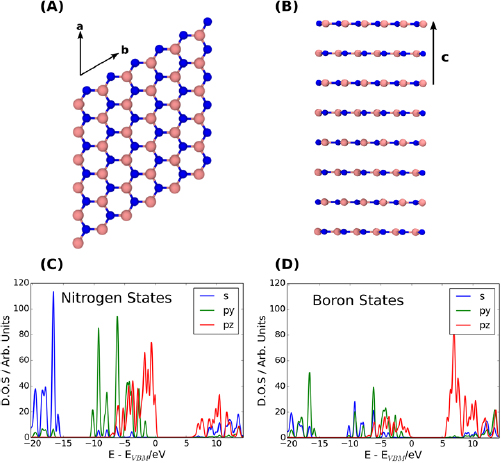
Figure 1. (A) A layer of hBN in the bulk. hBN has a honeycomb structure similar to graphene. (B) Side-view of the hBN simulation cell, showing the layers. (C) The N PDOS projected onto s orbitals and p orbitals of different orientation. (D) The B PDOS projected onto s orbitals and p orbitals of different orientation. In (C) and (D) the p x and p y spectra are identical, so only p y is shown for clarity.
Download figure:
Standard image High-resolution imageIt can be seen in figures 1(C) and (D) that the top of the valence band is predominantly formed from N p z states and the conduction band—from B p z states. Both bands, however, show significant hybridization in line with the covalent nature of the bonding in hBN.
3.1.1. Position of the VBM and CBM with respect to the vacuum level.
In electronic devices, the charge state of a defect in an insulator depends on the position of the system Fermi level with respect to the insulator band edges. To find the VBM position with respect to the vacuum level we simulated a slab of hBN in a 3D PBC cell with a vacuum gap present. Comparing the VBM position of the insulator (relative to the vacuum level) with the measured metal electrode workfunction,  gives us a prediction for the valence band offset. Neglecting band bending

where  is the VBM energy eigenvalue referenced to the vacuum potential.
The VBM position relative to the vacuum level calculated using a five layer slab of hBN is 7.0 eV. The vacuum potential is taken to be equal to the electrostatic potential far from the slab. The CBM is located 1.3 eV below the vacuum level. This is in close agreement with ultraviolet photoelectron spectroscopy (UPS) results, which give a range of VBM levels of 6.98–7.35 eV below the vacuum level [39].
Typical electrode wavefunctions vary between 4–5 eV. For example, the workfunction of graphene ranges between 4.5 and 4.8 eV [40] (which gives a VBM offset of 2.2–2.5 eV). The workfunction of copper ranges between 4.46–4.94 eV [41, 42] (giving a VB offset of 2.5–2.9 eV).
3.2. Isolated defects in hBN
We first present the results for the  defect in hBN. Atomistic configurations of the
  defect in three charge states are shown in figure 2. The ground state of the neutral B vacancy is a doublet spin configuration, with the quartet being 0.3 eV higher in energy. In the bulk, any given B atom is surrounded by three N atoms which form an equilateral triangle. The ground state of
  defect, however, is surrounded by three N atoms forming an isosceles triangle. This asymmetric distortion reduces the defect symmetry from D3h to
  .
.
Figure 2. The B vacancy in three charge states. The N–N distances are given in  . The coloured surfaces indicate spin density, with yellow indicating positive spin density and green indicating negative spin density. In the neutral and −2 charge states the defect geometry has
  symmetry. The −1 charge state has D3h symmetry. The spin density iso-value is 0.03.
Download figure:
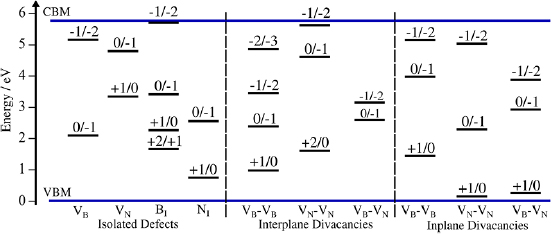
Standard image High-resolution imageThe formal charge state of the B vacancy ranges from −2 to 0. The CTLs are found to be at 2.1 eV and 5.2 eV, respectively (see figures 3 and 12). Using the VB offset value calculated for graphene, and neglecting band bending, we predict that the B vacancy will, in thermal equilibrium, be in its −1 charge state when hBN is interfaced with graphene.
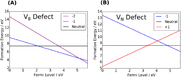
Figure 3. (A) Formation energy plot of the B vacancy in its charge states. (B) Formation energy plot of the N vacancy in its charge states.
Download figure:
Standard image High-resolution imageIn the −1 charge state, the ground state of the B vacancy is a triplet state (see figure 2), with spin density distributed equally across all three of the nearest neighbour N atoms. The N atoms also form an equilateral triangle. The −2 charge state is similar to the neutral charge state: the defect has  symmetry, the surrounding N atoms form an isosceles triangle and the spin configuration is a doublet.
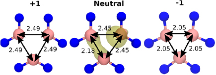
Figure 4. The N vacancy in its three charge states. Yellow surfaces indicate spin density. The +1 and −1 charge states are spin singlets. The neutral charge state is a doublet. All B–B distances are given in °A. The iso-surface value is 0.02.
Download figure:
Standard image High-resolution imageThe  defect has three charge states: −1, 0 and +1 (see figure 4). The
  geometry has D3h symmetry and its spin configuration is a singlet. Bader charge analysis gives a total charge of 0.8 localized onto each adjacent B atom. The
  ground state is a doublet. The nearest neighbour B atoms form an isosceles triangle, with one of the B atoms displaced out of plane. The
  and
and  defects are both in a singlet spin configuration.
The CTLs of the  defect are 3.6 eV for the +1/0 CTL and 4.6 eV for the 0/−1 CTL. Thus, the CTLs for the
  defect are higher in the band gap than for the
  defects. This implies that, when interfaced with an electrode, such as Cu or graphene, (with a workfunction around 4.5 eV) B vacancies will likely be −1 charged and N vacancies will likely be +1 charged.
Figure 5 shows the configuration of the neutral B interstitial (B ). The interstitial B atom (in all charge states) sits between two layers, directly between an N atom and a B atom. The ground state spin configuration of the neutral state is a doublet.
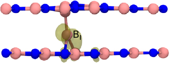
Figure 5. The neutral B interstitial. The BI interstitial sits between two layers. The spin density iso-surface value is 0.01.
Download figure:
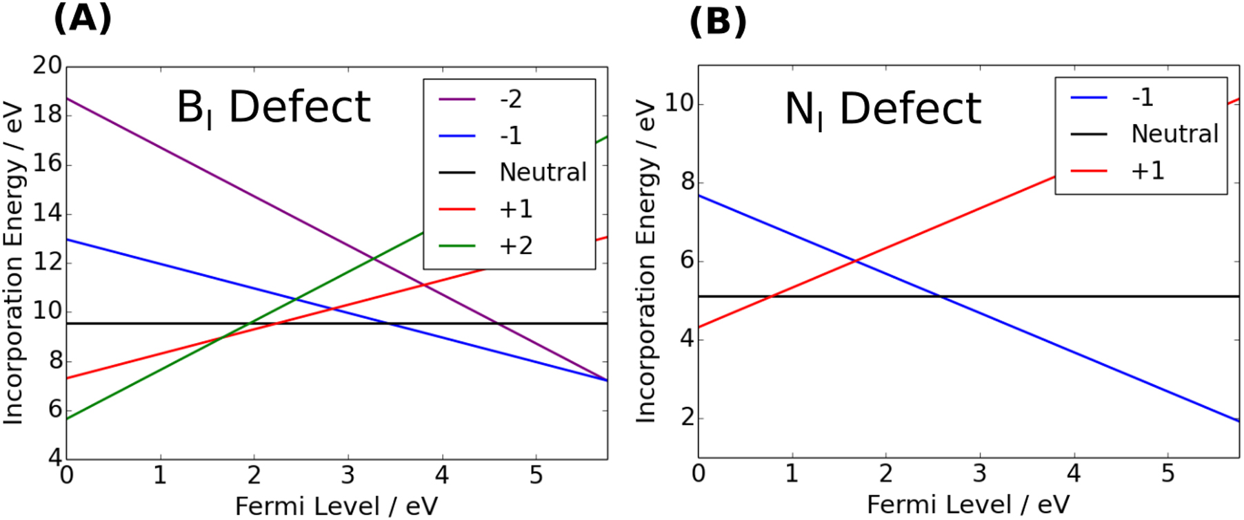
Standard image High-resolution imageThe BI defect can exist in five charge states, ranging from −2 to +2. Charging outside this range simply occupies (or vacates) perturbed band states. Figure 6 shows the formation energy of the BI defect as a function of the Fermi level position. Many of the CTLs lie close to typical metal Fermi level positions. This means that BI defects could be involved in electron or hole exchange with electrodes in devices. For example, the +1/0 and 0/−1 fall within the window of Fermi levels discussed in section 3.1.1.
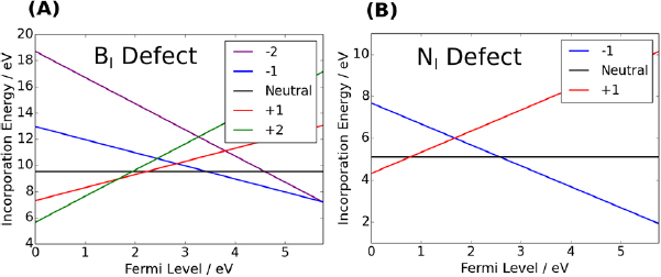
Figure 6. (A) The incorporation energy of the B interstitial is its possible charge states. (B) The incorporation energy of the N interstitial in its possible charge states. Crossover point indicate the CTLs.
Download figure:
Standard image High-resolution imageIn the +1 charge state of the BI defect, the singlet and triplet energies are too close to be distinguished using DFT (0.01 eV). In the singlet state, the charge of the B interstitial is +1. Positively charging (removing electrons from) the neutral B interstitial decreases the separation between the interstitial atom and the adjacent BN honeycomb plane. Removing a single electron shifts the interstitial 0.08  closer to the plane, whereas removing a second electron shifts the B interstitial by another 0.5
  closer to its nearest honeycomb plane. The +2 charge state of the B interstitial is in a doublet configuration. The −2 and −1 charge states are in the doublet and singlet configurations, respectively.
The neutral N interstitial is shown in figure 7. Unlike the BI defect, which sits approximately halfway between the layers, the NI defect sits close to one layer, 1.5  away from its nearest N neighbour. Unlike similar work conducted in [16], where the 0, −1 and −2 charge states of the NI defect are found to be stable, we find that these are in fact the −1, 0 and +1 charge states. The N
 , N
, N and N
and N defects are in a triplet, doublet and singlet spin state, respectively. Adding an electron to the N interstitial causes some of the surrounding B atoms to be pulled slightly out of plane, causing N–B separation to be reduced by as much as 0.8
  . Additionally, the NI defect forms a dimer of length 1.43
  with its nearest neighbour N atom. The N
 state seems to have the most minimal effect on the surrounding structure (there are not as many significant displacements relative to the bulk). In the +1 charge state, the NI defect sits 1.4
  away from its nearest neighbour N atom. Therefore, it is the case that in all the charge states of the N interstitial defect an N–N dimer is formed. Owing to the stability of the N–N bond, this should lead to increased stability of the NI defect. In fact, it can be seen in figure 6 that the incorporation energy of an N interstitial is much lower than that of a B interstitial for the given choice of chemical potential. The positions of charge transtion levels of individual defects in the band gap of hBN are summarised in figure 12.
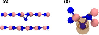
Figure 7. (A) The neutral N interstitials and its two adjacent layers. The N interstitial sits closer to one layer, and is separated from in nearest neighbour N by 1.5  . (B) Shows the surrounding structure of the N interstitial. The orange surface shows an isosurface = 0.01 of the spin density.
Download figure:
Standard image High-resolution image3.3. In-plane divacancies in hBN
Divacancies in hBN can exist in two main configurations—in-plane and inter-plane. The in-plane B divacancy is shown in figure 8. The singlet-triplet splitting is on the order of meV, and thus the singlet and triplet states are practically degenerate in our calculations.
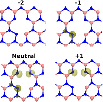
Figure 8. The B divacancy in different charge states. Spin density isovalues of 0.01 are indicated by the yellow surface. In the neutral case, the triplet state is shown, however, the singlet state is equal in energy and geometric configuration. In all charge states of the B divacancy, a N atom has replaced one of the missing B atoms, and has formed N–N bonds.
Download figure:
Standard image High-resolution imageWhen forming an in-plane B divacancy, there is one N atom which has two bonds broken, and 4 N atoms with one bond broken. As can be seen in figure 8, the N atom with 2 dangling bonds moves to a location previously occupied by a B atom and forms bonds with two neighbouring N atoms (both of which were previously bonded to a shared B atom). These two N–N bonds (of length 1.38  ) greatly stabilize the divacancy. The binding energy, calculated as
  , is equal to 4.9 eV. Surplus electrons localise onto the N atoms of the divacancy (figure 8). The −1 charge state is a quartet, but is only lower in energy than the doublet by 0.05 eV. The −2 charge state is a singlet spin state (the singlet-triplet splitting is 0.7 eV). The positive charge state is a doublet and has spin distributed across two of the N atoms (figure 8). The +1/0, 0/− 1 and −1/− 2 CTLs are located at 1.4, 4.0 and 5.1 eV above the VBM, respectively (see figure 12).
The neutral in-plane N divacancy is shown in figure 9. Removing two N atoms creates a B atom with two dangling bonds. This atom moves to form a bond with an adjacent B atom. The binding energy of the N divacancy is 2.9 eV. This is much lower than the binding energy of the B divacancy. This is due to the fact that, in the B divacances, N–N bonds are formed which are more stable than B–B bonds.
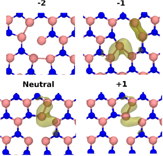
Figure 9. The N (inplane) divacancy in four different charge states. Transparent surfaces show the spin density (isovalue = 0.02). Vacancy binding is facilitated by the formation of B–B bonds.
Download figure:
Standard image High-resolution imageThe ground state of the neutral N divacancy is a triplet, which is by 1.4 eV lower in energy than the singlet state. Removing a N atom creates a B atom with two B neighbours (see figure 9). This B atom has a magnetic moment of 1  . The rest of the spin density is distributed over a number of B atoms. In the −1 charge state, also shown in figure 9, the quartet is by 0.95 eV more stable than the doublet. Spin density is spread over the B atoms adjacent to the divacancy. The B atom neighboured by two B atoms has a magnetic moment of 1
  . Other B atoms surrounding the vacancy have magnetic moments ranging from 0.2 to 0.4
  . The ground state of the N-divacancy in the +1 charge state (see figure 9) is a spin doublet, with the quartet spin state being 2.6 eV higher. The spin density is mostly distributed around three B atoms, as shown in figure 9. The largest proportion of the spin density is, again, localized on the B atom which is 2-coordinated with respect to B. This B atom has a magnetic moment of 0.4
  . The +1/0, 0/−1 and −1/−2 CTLs are located at 0.1, 2.3, and 5.0 eV above the VBM, respectively (see in figure 12).
The above discussion argues that the formation of N–N bonds in B divacancies are a cause of their strong binding. This trend continues for B trivacancies. The calculated total energy of a trivacancy is 4.8 eV lower than the energy of a well-separated vacancy and a divacancy. This is very close to the binding energy of the divacancy and we argue it is caused by the formation of another two N–N bonds. It can therefore be expected that, as larger B vacancy clusters are formed, more N–N bonds should also form and that B polyvacancies should, in general, be strongly bound.
Finally we analyse the in-plane  defect. The interaction between the B and N vacancies is very strong, with the neutral
  defect having a binding energy of 6.4 eV. In total, there are four stable charge states (from +1 to −2). We have found that the +1/0 CTL is only 0.26 eV above the VBM. The 0/−1 CTL is 2.9 eV above the VBM and the −1/−2 CTL is 3.9 eV above the VBM. Interestingly, although the B and N vacancies are in the same plane, molecular bridges
  planes form in some charge states. For example, in the −2 charge state, no planar arrangement of the defect is stable, and instead two B–N bridges connect to the adjacent layers (See figure 10). The ground state of the −1 charge state is similar, however, only one B–N bridge forms.
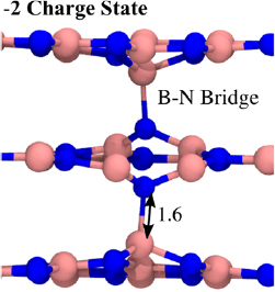
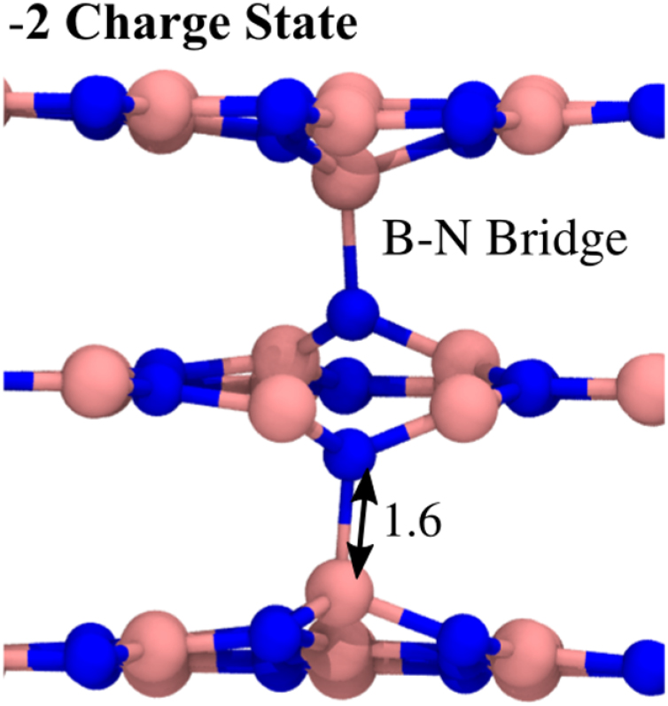
Figure 10. The −2 charged in-plane  defect in hBN. Although the missing B and N atoms are from the same plane, there is still significant interaction between the adjacent layers. The vacancies are present in the center layer, and are connected to the layers above and below by B–N molecular bridges. The bond length of the B–N connection is 1.6
  . There is no spin density and the ground state is a singlet.
Download figure:
Standard image High-resolution image3.4. Inter-plane divacancies in hBN
Vacancies in  hBN layers can also interact. We have considered an inter-plane arrangement where two vacancies sit across adjacent layers. For the inter-plane B divacancy, there are two possible configurations: a noninteracting 'simple' divacancy, which is just two vacancies separated across layers with no other bond breaking or forming, and a 'bridged' configuration, where a N–N bond forms across the layers (see figure 11(A)). The formation energy of the neutral simple inter-plane B divacancy is almost the same as that of two infinitely separated
  defects. One can consider this divacancy as two close but noninteracting single B vacancies. The whole divacancy is in a singlet state, but each individual vacancy is in a doublet spin configuration (with opposite spin orientation to one another). Each vacancy has three holes distributed around its surrounding N atoms.
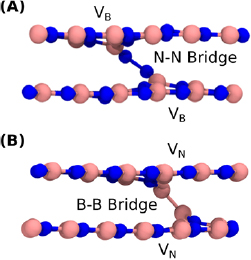
Figure 11. (A) The N-bridged B divacancy. Two adjacent B vacancies separated across layers are connected by a N–N bridge. (B) The B-bridged N divacancy. Two adjacent N vacancies, separated across layers, are connected by a B–B bridge.
Download figure:
Standard image High-resolution imageThe bridged configuration is 0.4 eV lower in energy in the neutral charge state. The N–N bridge greatly distorts the surrounding structure with the neighbouring B atoms displaced by 0.5  . Distortions of this size are usually energetically costly, however, the formation of the bridge is still energetically favourable due to the strength of the N–N bond. The N–N bond length is 1.47
  . In total, we find five charge states, ranging from +1 to −3. The +1/0, 0/−1, −1/−2 and −2/−3 CTLs are 1.0, 2.4, 3.3 and 4.8 eV above the VBM, respectively (see also figure 12). Spin states are indicated in table 1. The neutral inter-plane N divacancy only exists in the bridged configuration (figure 11(B))—we have not been able to find a stable simple configuration. The B–B bond length is 1.81
  . Since the bond is longer, the B atoms are not as significantly displaced out of the honeycomb plane as the N atoms are in the B divacancy. In the N divacancy, the B atoms (forming the B–B dimer) sit approximately 1
  out of plane. In the B divacancy, however, the N atoms which form the N–N dimer sit 1.2
  out of plane. Overall, the distortions surrounding the molecular bridge in the N divacancy are slightly smaller (approximately 0.1–0.2
  ) than those in the B divacancy. The +1 charge state is metastable in the
  defect, leading to a CTL between the +2 and 0 charge states, which is 1.6 eV (above the VBM). We also calculate the −1 and −2 charge state, with the 0/−1 CTL being at 4.6 eV and the −1/−2 CTL being at 5.6 eV above the VBM (see figure 12).
Table 1. The multiplicity of each defect, for each charge state. Charge states (from positive to negative) are shown on the left column and the respective multiplicity is indicated on the right. Multiplicity is abbreviated, for example S = Singlet and Q = Quartet. Where degeneracies are found (difference in energy between spin states <0.1 eV), both spin states are shown, separated by a dash.
| Defect: charge states | Multiplicity |
|---|---|
| Isolated defects | |
 : 0, −1, −2 : 0, −1, −2 |
D, T, D |
 : +1, 0, −1 : +1, 0, −1 |
S, D, S |
| BI: +2, +1, 0, −1, −2 | D, S-T, D, S, D |
| NI: +1, 0, −1 | T, D, S |
| Interplane divacancies | |
 : +1, 0, −1, −2, −3 : +1, 0, −1, −2, −3 |
D, T, D, S-T, D |
 : +2, 0, −1, −2 : +2, 0, −1, −2 |
S, S, D, S, |
 : 0, −1, −2 : 0, −1, −2 |
S, D, S |
| Inplane divacancies | |
 : +1, 0, −1, −2 : +1, 0, −1, −2 |
D, S-T, D-Q, S |
 : +1, 0, −1, −2 : +1, 0, −1, −2 |
D, T, Q, S |
 : +1, 0, −1, −2 : +1, 0, −1, −2 |
D, S, D, S |
Figure 12. The CTLs of the single intrinsic defects and divacancies in hBN.
Download figure:
Standard image High-resolution image
Inter-plane configurations of the  were also studied. Three charge states were found (0 to −2). Similar to the inter-plane N and B divacancies, molecular bridges also form between the vacancies. It is therefore the case that any
  defect, whether it is inter- or in- plane, can form molecular bridges which distort the local structure. The 0/−1 and −1/−2 CTLs are 2.6 and 3.1 eV above the VBM, respectively, as shown in figure 12.
4. Conclusions
We have calculated the structure and electronic properties of a range of intrinsic point defects in hBN. The CTLs of these defects are summarised in figure 12 and span the full band gap. Therefore, some of these defects will be capable of capturing carriers in hBN devices, depending on the workfunction of the electrode. We note that our results for isolated defects mostly agree with the HSE-based results in [16], however a small number of CTLs differ by approximately 0.5 eV, and there are other disagreements which were discussed in section 3.2. We note that compared to [16] we use larger cells, which should improve results with regards to reducing finite-size errors and more fully accommodating defect-induced lattice distortions.
Furthermore, it has been found that in-plane B polyvacancies have very high binding energies due to the formation of strong N–N bonds. The in-plane  divacancies and divacancies composed of vacancies on adjacent layers are stabilized by the formation of inter-layer molecular bridges, which significantly distort the surrounding atomic structure. These strong distortions lead to bond weakening and may serve as precursors to further propagation of structural degradation. These results provide valuable insight into the properties of defects which may affect the performance of hBN based electronic devices.
Acknowledgments
We acknowledge funding provided by the UK Engineering and Physical Sciences Research Council (EPSRC) under Grants No. EP/K01739X/1 and EP/P013503/1 and by the Leverhulme Trust RPG-2016-135. JS is funded by EPSRC Grant No. EP/G036675/1 to the Center for Doctoral Training. Computer facilities on the ARCHER UK National Supercomputing Service have been provided via the UKs HPC Materials Chemistry Consortium (EPSRC Grant No. EP/L000202). We would like to thank M Lanza, K-L Pay and A Ranjan for useful discussions and sharing the results of their work.