

Abstract
The production of hydrogen fuel through sunlight-driven water splitting has the potential to harness and store large quantities of solar energy in a clean and scalable chemical state, suitable for later use in a range of energy applications. Silicon (Si) possesses many of the required properties to be used effectively as a photoelectrochemical (PEC) water-splitting photoanode. However, its sensitivity to corrosion during the oxygen evolution reaction limits its performance in photoanode applications, thus requiring additional overlayer materials to protect the underlying Si substrate. Nickel oxide (NiO) is one material that acts as an effective protective layer, being transparent, suitably conductive and stable. In this work, we present NiO deposition via state-of-the-art atomic layer deposition and photoemission studies to grow and characterize NiO and Ni–metal protective films. Early-stage nucleation of deposited thin films is illustrated along with the effects of post-deposition annealing and argon milling on depth profile information. Previous reports on the effects of slow argon milling are explored and counter arguments are proposed. Protective films are subjected to PEC testing, which shows enhancement of stability and photocurrent output as a result of the deposited films and plasma annealing on these thin films.
Export citation and abstract BibTeX RIS

Original content from this work may be used under the terms of the Creative Commons Attribution 4.0 license. Any further distribution of this work must maintain attribution to the author(s) and the title of the work, journal citation and DOI.
1. Introduction
With the ever-growing challenges of climate change and energy security comes the need to move away from our dependence on the rapidly depleting supply of fossil fuels. Looking to more renewable sources, it is clear that the most abundant source of energy available to us is the sun. If harvested and stored at 100% efficiency, the Earth's electricity demands for a whole year could be met in just 1 h [1]. The main downfall of solar energy, as is the case with many sources of renewable energy, is its intermittency and seasonal variability making relying upon it to meet our energy demands difficult and impractical day to day. Therefore, it is necessary to develop energy storage techniques during times of excess availability for use in low-generation periods.
The conversion from solar energy to chemical fuel is an attractive storage technique that has the potential to store vast quantities of energy in an on-tap source that can be used in a wide range of industries and applications. Hydrogen is an example of a suitable chemical fuel partially due to its high mass-specific energy density and benign combustion byproducts, it can also be produced indirectly through electrolysis or directly through semiconductor based photoelectrochemical (PEC) water splitting [2].
The most important components of a PEC system are the photoelectrodes. The ideal photoelectrode candidate material must fulfill several important tasks at once in order to be suitable. These include good charge separation and transport, sufficient light absorption and the evolution of either hydrogen or oxygen at its surface. Furthermore, stability in the aqueous electrolyte solution with low material and production costs are also key in the development of this method of hydrogen production. It is unlikely for one semiconductor material to possess all of these exacting requirements to the level needed and as such trade-offs must be made, as well as exploring the fabrication of composite photoelectrodes wherein multiple materials are used in tandem with each carrying out specific complementary functions [3].
The field of water splitting has been studied extensively and silicon (Si) is commonly utilized as the base substrate for the PEC photoanode. Si is abundant and therefore a comparatively low-cost material that has a number of the necessary properties required for a suitable photoanode, such as favorable light absorption, high carrier mobility and band edges that make it suitable for both water oxidation and reduction, with an applied bias [4]. The primary obstacle with Si is its susceptibility to photoanodic corrosion during the oxygen evolution reaction (OER), resulting in the oxidation/passivation of the anode during operation, thus drastically reducing or totally halting performance [5, 6]. In order to enhance the performance of the PEC cell, materials to extend usable lifetimes and overall photocurrent output are required to prevent this photocorrosion so that it can be a viable competitor in energy production going forward.
One route to this is the application of a protective layer that distances the OER from the Si anode itself, thus preventing or eliminating the photocorrosion. Transition metal oxides, such as WO3 and TiO2, are suitable materials for this protective layer as they are more stable in the PEC electrolyte environment; however, they suffer from poor PEC activity. Applying layers of oxides, such as those named above as protective, and in some cases catalyst, layers on Si has been studied and are shown to achieve marginal gains in terms of photoanode stability in a protective capacity alongside performing as an electrocatalyst enhancing the photocurrent output [7].
Materials of interest for semiconductor water splitting are split into platinum group metals (PGMs) and non-PGMs (NPGMs), with PGMs offering superior performance making them excellent choices for co-catalyst or counter electrode applications [8, 9]. However, their high cost and limited availability render them undesirable choices for large-scale implementation [8]. Thus, NPGMs are more economically viable, with Ti, Ni, Cu and Zn being among the most effective. Although exhibiting reduced performance compared to their PGM counterparts, utilization of such materials in conjunction with substrate morphology modification as well as post-deposition film treatment can improve the performance of such materials in their as deposited state [8].
Since the first demonstration in 1972 by Fujishima and Honda on the use of TiO2 as a photoanode, it has been clear that photoelectrodes used in water splitting must be combined with an additional catalyst layer, such as IrO2, Ni-Fe or Pt, in order to maximize performance [10–12]. Reports on TiO2 have shown that there is room for alternative materials to improve on early advancements and findings from TiO2 studies to increase both film stability over increased operation time-frames and gross photocurrent generation [4, 7, 13].
Nickel oxide (NiO) has attracted a great deal of attention for its use in PEC water splitting as well as a hole transport layer for perovskite solar cells (PSCs) thus warranting additional understanding of its growth chemistry and performance characteristics [14, 15]. The effect of post-deposition annealing treatment parameters and their implication on film properties and subsequent performance is also of interest in such fields [16]. Interest in NiO in the fields of PSCs and PECs stems primarily from its ability to provide enhanced device stability, decreased absorption losses and its ease of deposition, commonly achieved using plasma-enhanced atomic layer deposition (PEALD) [17]. Furthermore, its suitably wide bandgap of 3.4–4 eV light transmission coupled with a suitable energy level alignment that facilitates hole transport makes this transition metal oxide one of relevance within the field [18].
Pulsed laser deposition, spin coating, sputtering and atomic layer deposition (ALD) are common methods of NiO film preparation previously reported in the literature, with spin coating being the more common approach due to its comparative simplicity and equipment requirements [19–22]. However, spin coating falls short in offering a high level of controllability of film thickness as well as poor surface coverage and wettability, particularly when the base substrate is especially rough, resulting in the introduction of interfacial defects [16, 23].
Both pulsed laser deposition and sputtering are prone to the formation of pinholes throughout the films resulting in undesirable performance for PEC or PSC applications [24]. As a result of the above mentioned shortcomings of these different film deposition techniques, ALD emerges as an attractive alternative owing to its layer-by-layer self-limiting deposition, which results in a high level of controllability both in terms of film thickness and properties at the atomic level [25–29]. The sequential admittance of vapor-phase ALD products to the deposition chamber enables highly controllable and conformal film growth [26, 29].
Therefore, ALD has become a favorable technique for the fabrication of thin films on non-planar surfaces due to its conformality, allowing for depositions on textured surfaces or those with complex surface morphology such as multiwalled carbon nanotubes and fullerenes among others [30–32]. This work details an in-line x-ray photoelectron spectroscopy (XPS) analysis of the growth of bulk Ni films with additional focus on the nucleation of ultra-thin (ca. 2 nm) Ni films on Si using Bis(cyclopentadienyl)nickel(II) or nickelocene as the chosen precursor. Films were grown via PEALD. The effect of various growth parameters, such as deposition temperature, reactant and co-reactant dose times, are detailed.
Films are characterized using in situ XPS to avoid undesirable and often misleading effects of atmospheric contamination of deposited films. Nucleation of NiO was studied through a sequential growth experiment that involved performing a half cycle of ALD followed by XPS scanning. This was repeated for every half cycle up to five ALD cycles in total, then proceeding with regular full cycles for the remainder of the film deposition. This approach allows for the analysis of the early-stage growth at the Ni–Si interface during the first five cycles.
Argon milling was also utilized to study and confirm the composition of deposited NiO films. Analysis of the impact of post-deposition plasma annealing treatments on film stoichiometry and electrochemical performance is shown in addition to that of plasma annealing steps interspersed within the film growth recipe in so-called supercycles.
The effect of applying post-deposition annealing treatments to deposited films as well as the optimization of the deposition recipe used in the study are also presented. There is little to be found in literature reports on the performance of Ni–metal in water-splitting applications and as such this has been explored to determine its efficacy. Deposited oxide and metal films are tested under simulated sunlight conditions to study their performance as water splitting photoanodes for the production of hydrogen fuel.
2. Experimental
2.1. ALD of NiO
n-Si (100  –
– ) N(Phos)-doped reclaim-grade wafers were purchased from PI-KEM Ltd The 4 in diameter Si of center thickness from
  –
– were cleaved into
  squares before being loaded into the ALD system in their as-received state after being blown with N2 to remove Si particles created during the cleaving. NiO deposition was performed via PEALD in a commercial grade Oxford Instruments FlexAl ALD Reactor (base pressure
  ) using Bis(cyclopentadienyl)nickel(II) (nickelocene STREM 99%) and a 300 W O2 plasma as the reactant and co-reactant species respectively, with N2 as the carrier gas. The system uses a radio frequency generated inductively coupled plasma with an excitation energy of 13.56 MHz. A 300 W hydrogen plasma of varying duration was applied for mid-recipe and post-deposition annealing where required. Substrate temperatures of 200, 250 and 300°C were applied to determine the ALD window for nickelocene in the reactor.
Reactant dose lengths of 0.25–5 s were investigated to establish precursor dose saturation, while O2-plasma steps of 1–15 s were similarly tested. Growth per cycle (GPC) rates were also determined using these parameters, shown in figure 1. These saturation curves and GPC rates combined with ALD tool manufacturer suggested parameters and literature reports aided in the selection of final process parameters used for subsequent sequential and continuously grown films. A form of sequential 'supercycling' was carried out in an effort to explore methods of depositing Ni–metal. The supercycle involved four standard ALD cycles of reactant and co-reactant using finalized parameters shown in figure 1, followed by a 5 min 300 W H2 plasma anneal. The precursor bottle, manifold, lines and chamber walls were set to 90, 65, 75 and 120 °C respectively.

Figure 1. ALD process parameters used for the deposition of thin films in this study with a substrate temperature of 250 °C.
Download figure:
Standard image High-resolution imageThis series of four deposition steps and one annealing step was continued for a total of 20, 40, 80 and finally 120 cycles with XPS scanning performed between these steps to study the film formation during its growth. The same was performed with XPS scanning only following the full 120 cycles. A deposition of 250 cycles with identical parameters to those used in the 120-supercycle process was carried out; however, cycles were completed in 50 supercycle batches with 15 min of plasma annealing performed following each 50 cycles and scanned after each annealing step. Again, the same 250-cycle process was subjected to the same total amount of annealing of 75 min at the end of the deposition to compare the effect of the same amount of annealing time at the end of deposition versus interspersed in the deposition and its effect on the resulting films.
2.2. Characterization techniques
In-line photoemission analysis was performed on film post deposition as well as post plasma annealing treatments and PEC cell testing. XPS allowed for the determination of film composition as well as a method of real time thickness approximation. XPS was carried out using a Scienta Omicron (Monochromated Al Kα source 1486.74 eV,  base pressure) with a 128 channel Argus CU detector. The XPS is coupled via a vacuum held robotic wafer transfer system allowing for sample transfer between XPS and ALD in less than 1 min without the need for vacuum break and unwanted contamination of wafer surfaces. Wide energy survey spectra as well as high-resolution narrow-window spectra were taken with step sizes of 1 and 0.1 eV respectively. Analysis was performed using an analyzer peak fitting software with a Shirley–Sherwood background and Voigt profiles applied [33]. All spectra were shifted such that the Si0 2p3/2 component was placed at 99.4 eV binding energy [34,35].
Thickness values were approximated mathematically using the Thickogram method [36], which by measuring the suppression of the substrate peak as a function of the deposition of an overlayer and knowing material properties such as the electron mean free path allows for thickness approximations. A method was derived to compare the peak intensity of a substrate and the overlayer peak for a given take-off angle, which when combined with the effective attenuation lengths (EAL) of the materials in question allows for the determination of the thickness of the overlayer based on the mean free path of the substrate electrons in the overlayer material. The EAL values were obtained from the NIST EAL database, with the XPS relative sensitivity factors being taken from the database of empirically derived atomic sensitivity factors [37]. In order to verify the accuracy of the Thickogram method, film thicknesses were also measured using an ex situ ellipsometer, which showed that the Thickogram-obtained thickness approximations were satisfactory. Spectroscopic ellipsometry was carried out using a Woollam XLS-100 multi-wavelength system. Slow Ar milling was performed at 3.5 k eV at a pressure of  with filament current (175 V grid, L1 0%, L2 70%). XPS scans were carried out after 0, 2 4, 6, 8, 13, 18, 23 and 33 min of milling using a Focus GmbH FDG 150 ion source.
PEC cell testing of the films in order to measure chemical stability and photocurrent output was carried out in a Redoxme AB MM 15 ml double-sided PEC cell (PEEK constructed body, in three-electrode configuration) with Pt counter electrode (99.9%) and a Ag/AgCl (1 mol KCl−1) reference electrode. The electrolyte solution used was a 0.5 M phosphate buffer solution (pH 7.4) with the electrodes being irradiated with 1000 Wm−2 AM 1.5 G simulated sunlight supplied by an Oriel Instruments xenon arc lamp. Samples were irradiated in the PEC cell in a top-down configuration with 1 cm2 of exposed sample surface. I–V linear sweep voltammetry PEC tests were performed to determine the photocurrent density of deposited films and to screen their effectiveness as photoanode materials with this test sweeping from −0.7–3.5 V versus Ag/AgCl. Samples were also subjected to chronoamperometric testing at 1 V vs Ag/AgCl for 1000 s, such as to determine the chemical stability of films under PEC conditions.
3. Results and discussion
3.1. XPS characterization
3.1.1. Cycle-by-cycle growth chemistry.
XPS was carried out on Ni films at all stages of deposition and treatment from as deposited, post plasma annealing and subsequent exposure to atmosphere such as to investigate the state of Ni films in these environments before any PEC testing. Prior to depositing Ni films for characterization and later PEC testing, an investigation into acquiring optimal deposition parameters for the ALD FlexAl system, such as the NiCp2 dose time, was performed. The saturation point was determined using a combination of ex situ ellipsometry alongside the complementary Thickogram method of thickness approximation by monitoring the ratio of the Ni 2p overlayer peak with that of the substrate Si 2p peak analyzing its rate of attenuation as a function of increasing ALD cycles and therefore overlayer film thickness. An initial substrate temperature of 250 °C was chosen for characterization studies that is within the ALD window for PEALD of NiO from nickelocene and O2 plasma and provided a suitable starting temperature for nucleation studies [38–40]. This temperature was used during the acquisition of reactant and co-reactant saturation curves as shown in figure 2, such as to characterize the nickelocene precursor on the ALD system because variations in chamber geometry between ALD systems can influence film growth rates. It can be seen from figure 2 that film thickness increases sharply with increasing reactant dose time up until 3 s wherein the growth rate begins to diminish. Based on the dose saturation curve and owing to acceptable levels of carbon incorporation within deposited films of approximately 4%, reactant and co-reactant dose times of 1 s and 10 s, respectively were chosen for all further film depositions with the co-reactant dose of 10 s selected based on ALD recipes within the literature while yielding a suitable growth rate and film stoichiometry [41].
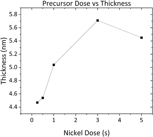
Figure 2. Nickelocene reactant dose time saturation curve for 100 cycle processes from 0.25 to 5 s doses, with the co-reactant dose time set at 10 s.
Download figure:
Standard image High-resolution imageIn an effort to gain further insight into the early-stage growth kinetics of the Ni deposition process, sequential PEALD depositions were performed and analyzed throughout the process at regular intervals using XPS. These measurements focused on the Si 2p, O 1s, Ni 2p3/2 and C 1s core levels, such as to closely monitor the film growth and to identify any evidence of additional oxidation states or silicides in the case of the Ni peak. The formation of oxidation states is of particular relevance due to the hole transport to the electrode surface relying heavily on the interfacial chemistry between the overlying Ni protective layer and the underlying Si substrate.
The characterization of the precursor within the ALD system allowed for the investigation of the nucleation of NiO thin films for a variety of substrate temperatures consisting of 200, 250 and 300 °C. Guided by literature reports and combined with investigations within this study at both higher and lower substrate temperatures, 250 °C was found to be the optimal deposition temperature. This is based on GPC deposition rate as well as stoichiometry evaluations finding remnant carbon incorporation to be in the sub 5% following variations in recipe parameters to reduce this and was therefore chosen for the remainder of the depositions performed throughout. The films used in the nucleation investigations were grown via sequential growth wherein half cycles consisting of just the reactant or co-reactant dose were carried out up to a total of five cycles, and five additional full ALD cycles were performed to reach a total of 10 cycles before carrying out 10 cycle batches up to the final sum of 100 cycles. In situ XPS analysis was performed on the sample after every half ALD cycle up to a total of five full ALD cycles, five additional cycles were performed before being scanned again at a total sum of 10 cycles, with XPS scanning being performed after every 10 cycles after this point to the final sum of 100 cycles. An example of these nucleation studies is shown in figure 3. It can be seen in figure 3(a) the sample shows measurable quantities of Ni following three ALD cycles from the elemental compositions obtained using XPS. These compositions were calculated using the XPS measurements seen in figure 3(b) which confirms this with the evolution of the Ni 2p3/2 peak as a function of increasing ALD cycles. Sequentially grown films allowed for the determination of GPC rates for the deposition recipe used which later facilitated accurate deposition of a desired film thickness.
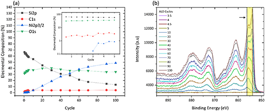
Figure 3. (a) Elemental compositions of 250 °C grown sample substrate with inset enhanced view of the initial half cycles. (b) High-resolution narrow energy region XPS spectra showing sequential growth of NiO with evidence of nucleation delay verified with growth undetectable before three ALD cycles with area highlighted indicating BE shift of Ni peak from early through to the final ALD cycle.
Download figure:
Standard image High-resolution imageXPS analysis of the sequentially grown Ni film shows that the first detectable Ni 2p signal appears at 856.1 eV following 3.5 ALD cycles and shifts gradually to lower BE over the course of the deposition to the position of NiO at 854.2 eV illustrated in figure 3(b), a BE position that is consistent with literature reports [41–44]. This BE shift over the course of the film deposition is indicative of the strong interaction between the early-stage monolayers of Ni atoms with the underlying Si substrate. A similar effect is observed in the Si 2p peak with the oxide BE position starting out at 103.6 eV for a bare untreated reference Si substrate which, over the course of the deposition, shifts to the lower BE position of 102.9 eV at the peak maximum. This shift of the oxide component in the Si peak is a further indication of the strong interactions between Si and Ni. The formation of suboxides at the Si–Ni interface results in the suppression of the bare Si oxide peak as a function of ALD cycles as the presence of these suboxides, silicates or silicides becomes dominant in that BE region. The extent of the BE shift of the oxide component of the Si 2p peak is illustrated in figure 4(a) wherein normalized XPS spectra of a bare Si reference sample are compared to that of 100 cycles of NiO as well as the tracking of the BE shift over the full course of the sequential deposition. Figure 4(b) tracks the BE shift of the Si oxide component as a function of ALD cycle, with the inset showing a detailed view of the early half cycles where we observe the BE of the oxide decreasing following each co-reactant pulse, while the reactant dose causes the BE to increase relative to the previous co-reactant half cycle. While counterintuitive, this suggests that NiCp2 doses promote a reaction at the interface, which causes the breaking of some Ni–O bonds, with the released oxygen bonding to Si. It is possible that this is accompanied by the formation of Ni–Ni bonds, but the Ni2p signal is too weak to confirm this. Subsequently, during the oxidation step the donation of oxygen to nickel and reduction of the silicon oxide appears to be occurring. The similar electronegativity of Si and Ni and the instability of the respective suboxides support the hypothesis that oxygen is routinely transferred between the elements. These results were observed for all substrate deposition temperatures of 200, 250 and 300 °C.
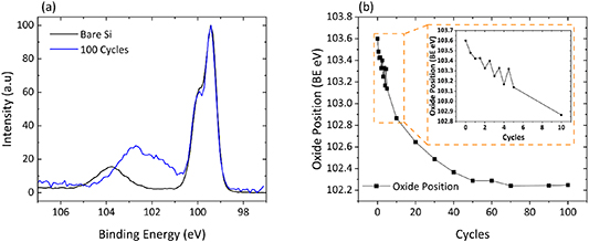
Figure 4. (a) Normalized XPS spectra of bare reference Si substrate versus 100 cycles of NiO (b) Si 2p oxide BE as a function of Ni ALD cycles.
Download figure:
Standard image High-resolution imageThe evolution of the O 1s peak is depicted in figure 5 as a function of increasing number of ALD cycles for the same sequentially grown samples. In the O 1s spectrum the two primary peaks observed are at approximately 533 eV corresponding to oxygen present in the substrate and 529 eV as a result of the oxygen in NiO. The intensity of the O 1s peak corresponding to SiOx can be seen to rapidly decrease as it is attenuated as early as the first half of the ALD cycle and then increases, while shifting to lower BE, indicating significant restructuring at the interface with the substrate. At lower BE, the NiO contribution is seen to increase steadily throughout the deposition, becoming measurable after approximately 10 full cycles.
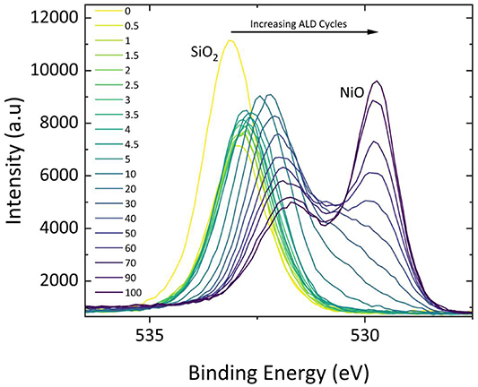
Figure 5. O 1s XPS high-resolution spectra as a function of increasing ALD cycles for sequentially grown NiO at 250 °C substrate temperature.
Download figure:
Standard image High-resolution image3.1.2. Post-deposition annealing to form metallic Ni.
The films were removed from vacuum and stored in atmosphere before being rescanned to determine the extent of atmospheric contamination, prior to being subjected to a series of plasma annealing stages in an effort to reduce the film to Ni–metal. A 20 and 40 min 300 W H2 plasma anneal was carried out at 250 °C with in situ XPS analysis performed before and after. Samples were removed from vacuum and exposed to atmosphere then reloaded for XPS analysis one final time to determine the extent of sample contamination and susceptibility to carbon incorporation post plasma annealing.
Figure 6 shows the XPS spectra throughout all stages of treatment. The high-resolution spectra of the Ni 2p peak verifies the presence of NiO with the peak centered at 854.2 eV, as expected shown in figure 6(a). Films subjected to H2 plasma annealing for 20 min are largely reduced to metallic nickel as shown in figure 6(a) with the Ni 2p3/2 BE centered at 852.9 eV separated by 18 eV from the Ni 2p1/2 component at 870.1 eV. The Ni metal 2p3/2 peak is observed at 852.9 eV, which falls within the literature range of 852.7 eV ± 0.4 eV [45, 46]. Following the 40 min H2 annealing there are no significant improvements in the reduction of the film seen compared to the 20 min process, but rather results in a considerable etching effect on the film shown by the reemergence of the Si 2p peak following this treatment. Additionally, the 40 min annealed sample appears to reintroduce the presence of the NiO component seen in the as deposited state at 854.2 eV and 861.2 eV, which may suggest that although receiving an extended plasma annealing stage, 20 min was not sufficient to reduce the bulk film in its entirety. It is clear from the 20 min plasma annealed sample that there are remnants of the NiO features in the Ni 2p3/2 component still present which further indicates that the film was not fully reduced, potentially suggesting that some fully or partially oxidized nickel remains deeper within the film with only the surface of the Ni film being reduced fully. The 40 min annealed sample is seen to uncover these buried features by removing the overlying metallic Ni through film etching, which is confirmed as mentioned by the reappearance of the Si film upon completion, and uncovering the underlying Ni silicate, which appears more stable and therefore more difficult to reduce due to it remaining even following the extensive plasma annealing.
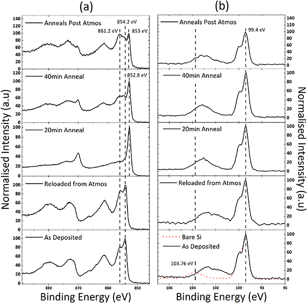
Figure 6. High-resolution normalized XPS spectra for all stages of treatment on the same sample: (a) Ni 2p; (b) Si 2p. In (b) the BE positions of the Si0 and Si4+ are shown for reference.
Download figure:
Standard image High-resolution imageFigure 6(b) shows the high-resolution spectra for the Si 2p region as a function of sample treatment over the course of the plasma annealing investigation with that of a bare Si sample included as a reference, all data have been shifted to align the bulk to 99.4 eV [34]. It is clear when looking at the as deposited film as well as that of the film post-exposure to atmosphere that there is a significant shift of the higher BE oxide peak to a lower BE suggesting the presence of additional Si oxidation states as seen from the deconvolution shown in figure S1. Starting from bare Si with the expected single 4+ oxidation state at 103.8 eV, the silicon oxide component in the as deposited film is seen to primarily comprise 3+ and 2+ oxidation states at 102.5 eV and 101.3 eV, respectively, with that of the 4+ being diminished almost into the noise. Upon exposure of the film to atmosphere, the 4+ is entirely suppressed and the emergence of the 1+ state at approximately 100.6 eV becomes apparent. 20 min of plasma annealing is sufficient to remove this 1+ oxide component and only that of the 2+ and 3+ components are observed. The 40 min anneal, due to its etching nature, uncovers the underlying SiO2 and therefore we observe the reappearance of the 4+ oxide component.
Robust deconvolution of XPS spectra of Ni is found to be highly complex owing to the numerous satellite features present within the peak envelope in addition to their tendency to overlap one another making indisputable assertions about their identification difficult. This is reflected within the literature, with many reports presenting deconvolution of the Ni 2p3/2 region solely with little or no analysis of the Ni 2p1/2 region [46]. Furthermore, general consistency within the literature on the number of fit peaks within the envelope is lacking and there appears to be an acceptance of deviation of the data set and the fit envelope with it being cited as a result of the fit complexity of the Ni region [47–49]. As such, it is more reasonable to analyze XPS spectra of this region qualitatively rather than quantitatively due to the inherent unreliability. However, Biesinger et al present perhaps the most complete assessment of the fitting of the Ni region that was the basis and reference source utilized in this work for a satisfactory example of a Ni 2p3/2 deconvolution as seen in figure S2 showing only marginal deviation of the fit envelope from the data set [50]. Figure S3 shows deconvolution of high-resolution spectra for the remaining stages of sample treatment associated with the sample shown in figure 6.
3.1.3. Comparison between depth profiling by Ar milling and cycle-by-cycle growth.
Ar ion bombardment in conjunction with XPS is regularly employed as a method of depth profiling deposited thin films. In order to compare the depth profile information that our cycle-by-cycle approach yielded with the more traditional method, we carried out slow Ar milling coupled with XPS depth profiling on the same films. Figures 7(a) and (c) show XPS high-resolution Ni 2p spectra for a NiO film before and after slow Ar milling totaling 33 min. The data appear to show an overlayer of NiO, with metallic nickel metal underneath, with the predominant peak appearing at approximately 853 eV, the BE expected with Ni-metal rather than the 854 eV which is consistent with NiO. Ar milling was performed in short, repeated bursts to a total time of 2, 4, 6, 8, 13, 18, 23 and 33 min, with in situ XPS analysis after each. Figure 7(d) shows the BE shifts from a higher to a lower BE as a function of Ar milling time, indicating a greater metallic contribution as a function of time. This analysis is consistent with data from Kenney et al, wherein the film is reported to remain metallic below a thin layer of oxide, even following long duration PEC testing in a harshly oxidizing environment [5]. However, both our data and that of Kenney et al show no presence of metallic nickel before Ar milling, despite the entire film being well within the sampling depth of XPS. Our sequential growth studies have shown that the films under consideration are oxidized throughout the growth process, but Ar depth profiling suggests the presence of metal. NiO films have been shown within the literature to readily reduce to metallic Ni upon ion bombardment [51]. The reducing effect and the so-called preferential sputtering of oxygen in NiO and other transition metals and oxides such as Fe, Cu, Mo and V is widely reported with MoO3, V2O5, Fe2O3 and CuO being reported to reduce to MoO2, V2O3, Fe and Cu, respectively [52, 53]. Although an inert gas itself, Ar+ induces chemical reactions within the target material and as a result of the high sputtering yield and volatility of oxygen it is more likely to escape from a bombarded material than heavier atoms of the same material. As a consequence of these factors, the material undergoes a gradual reduction. However, the theoretical mechanisms of preferential sputtering in metal oxides are not well developed or agreed upon fully in the literature. This has previously been attributed to the diffusion of lattice oxygen alongside sputtering enhanced vaporization and thermal sputtering [54]. Thermal sputtering is that caused through the momentary temperature spike as a result of incident ions at the impact site. These impact-induced temperature spikes have the capability to result in a range of effects from disordering, stoichiometry alteration and primarily the sputtering effect [55]. A similar reducing effect observed within this work is illustrated by Chen et al wherein the reduction of the NiO film is observed following as little as 1000 s [56].
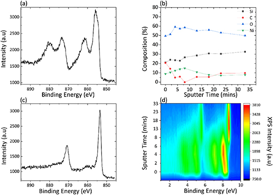
Figure 7. (a) and (c) XPS high-resolution spectra of argon-milled NiO in its as deposited and post 33 min of sputtering, respectively. (b) Elemental compositions as a function of argon milling. (d) Contour plot showing film conversion from nickel oxide to nickel metal as a function of increasing argon milling.
Download figure:
Standard image High-resolution imageFigure 7(b) tracks the elemental composition of the Ni film as a function of Ar milling time with values calculated using XPS. This shows the rapid removal of carbon during the initial milling stages with Ni simultaneously increasing during the early milling steps due to a reduction in its attenuation by overlying carbon. Following the first 8 min of milling, the Ni signal is seen to diminish due to the etch back of the Ni film. The Si peak is seen to increase consistently as the Ni film is milled away, exposing more of the underlying substrate, consistent with reports from Kenney et al [5]. Oxygen is seen to increase initially as C–C bonds are removed, uncovering the underlying NiO before the O in the NiO is preferentially removed, leaving behind Ni–Ni bonds with the remaining O being from SiO2 and the interfacial region of the Ni and Si. This comparison between live 'during growth' depth profiling and traditional Ar milling shows the risks in making assumptions about film chemistry using the latter approach.
3.1.4. Ni metal growth by annealing versus supercycles.
The majority of investigations into Ni with regard to water splitting applications detail only the performance of NiO [43, 57–61]. We therefore investigate the effect of Ni–metal on water splitting with metallic films deposited via supercycle deposition. It was observed through earlier investigations within this work that NiO films are readily reduced to Ni–metal through the application of H2 plasma annealing post-deposition. However, we endeavored to grow metallic Ni rather than forming it through the application of this post-deposition annealing. We compare the performance of metallic Ni films deposited in the traditional cycle-by-cycle ALD regime with post-deposition H2 annealing applied along with so-called supercycle depositions with H2 plasma annealing stages interspersed within the ALD deposition process. This supercycle regime was explored in order to ensure that all unreacted remnant carbon ligands were removed throughout the growth of the film. An additional motive for the investigation into supercycle depositions was to compare the reduction of films via post-deposition annealing of the bulk film as opposed to the reduction of several monolayers at a time and the effect, if any, of this on film stoichiometry.
The 120-supercycle and 120 post anneal samples yielded 2.85 nm and 3.18 nm, respectively, while the 250-supercycle and 250 post anneal yielded 5.63 nm and 6.43 nm. From figure 8(b) showing the high-resolution spectra for the Si 2p of the four variations of the supercycle samples, it can be seen that the 120-supercycle sample exhibits the least attenuated Si signal due to the marginally reduced GPC when compared to its 120 post anneal counterpart. Furthermore, the 120-cycle samples both show a reduction in the energy separation between the bulk and oxide peaks of the Si 2p region due to the reduced film thickness resulting in smaller attenuation of the lower BE oxidation states in the Si region. The reduced growth rate obtained through ellipsometry measurements is verified in figure 8(b) which shows the Ni 2p3/2 of the 120-supercycle sample to be decreased versus the 120 post anneal sample. The large attenuation difference seen in the Si peak is verified as being due to the enhanced growth of the Ni film when looking to figure S4 where the C1s contribution of the 120-supercycle and 120 post anneal samples are approximately equal. Figure S4 shows that as thickness increases the level of carbon incorporation within the film continues to rise regardless of whether it is deposited with interspersed plasma annealing steps or waiting for complete deposition before a final annealing stage.
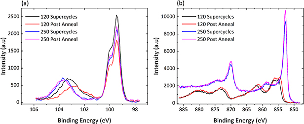
Figure 8. XPS high-resolution spectra showing the four supercycle samples in their as deposited state: (a) Si 2p; (b) Ni 2p3/2.
Download figure:
Standard image High-resolution imageFigure 8(a) shows the high-resolution spectra for the Ni 2p3/2 region wherein both the 250-supercycle and 250 post anneal samples are seen to form strong lower BE peaks consistent with the presence of Ni–metal. It also shows a similar trend for both of the 120-cycle samples with the post-anneal variant in both cases, demonstrating both enhanced growth and marginal but measurable shift to lower BE. Figure S5 shows XPS spectra for the 250-supercycle and post-anneal samples following exposure to atmosphere, wherein a rapid attenuation of the Ni 2p3/2 peak is observed alongside the conversion of the films from Ni–metal to NiO through the oxidation of the film with the post-annealed sample showing greater resistance to oxidation due to its greater thickness.
3.2. PEC Testing
Time-degradation PEC testing allows for the investigation of the stability of films under water oxidation conditions. Figure 9 shows the degradation measurements for the Ni-based films produced in this work with an applied voltage of 1 V versus Ag/AgCl equivalent to 1.65 V versus RHE and contrasts the application of post-deposition anneal versus the supercycle deposition with shorter plasma annealing stages carried out during the deposition itself. It can be seen that the application of the annealing treatment at the end of the ALD deposition is preferable in terms of gross initial photocurrent output. Despite achieving significant photocurrent output, both post-deposition annealed samples show a sharp decline over the course of the PEC test duration.

Figure 9. Chronoamperometric (time degradation; 1 V versus Ag/AgCl applied) photoelectrochemical cell testing of supercycle grown Ni films contrasting continuous (through) growth followed by plasma annealing with the supercycle method of interspersed plasma annealing stages during deposition. 120 Super: 120 total ALD cycles with interspersed annealing stages. 120 Post Anneal: 120 total ALD cycles with the annealing step performed at the end of the deposition. Degradation testing of a 5 nm NiO sample is also illustrated for comparison.
Download figure:
Standard image High-resolution imageThe supercycle samples exhibit drastically reduced photocurrent output, but this reduced output remains largely steady throughout the measurement, although at a very low level. This result suggests that enhanced film stability can be achieved through the application of annealing treatments throughout the deposition in the supercycle regime. This could mean that utilizing both film types, with post-deposition annealed Ni being suitable for the bulk of the film with a layer of supercycle deposited Ni on top to provide enhanced stability, could be beneficial for realizing a more efficient and stable water splitting anode, although not explored within this study. For reference and comparison, additional degradation measurements of 2 nm and 5 nm NiO films are also shown being that the 120 and 250 cycles are in the thickness range of 2 nm and 5 nm, respectively. It is clear that NiO films perform better in terms of gross photocurrent output alongside improved film stability at both thicknesses through beginning and finishing degradation testing with current output higher than that exhibited by the supercycle or post anneal samples, a result not previously seen within the literature.
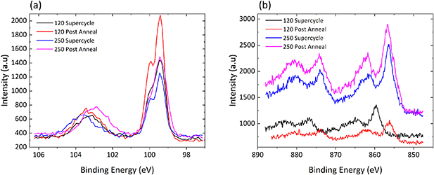
Figure 10 shows the XPS high-resolution Si 2p and Ni 2p3/2 spectra for the supercycle and post-anneal samples following testing in the PEC cell. The testing and results from figure 10(b) showing conversion from metal to oxide further verifies the inaccuracy of a previous report on the effects of Ar sputtering and the protection offered by a metallic overlayer to the underlying NiO [5]. Furthermore, it can be seen from figure 10(a) that the application of a post-deposition H2 annealing yields a reduced Si 2p bulk-oxide energy separation through the additional presence of sub-oxide states compared to that seen in the supercycle-deposited films. From figure 10(b) it is clear that PEC testing results in the complete oxidation of the Ni films. This result is most clear from the 250 cycle samples that exhibited highly metallic peak profiles in figure 8 when deposited; however, cell testing converts the film to NiO. Figure S6(a) shows that a highly metallic film even when exposed to atmosphere begins oxidizing, although not entirely. Only upon being tested under the harsh electrolyte environment of the PEC cell does the film entirely convert to NiO oxidizing throughout the film, as can be seen clearly in figure 10.
Figure 10. XPS high-resolution spectra showing the four supercycle samples following photoelectrochemical cell testing: (a) Si 2p; (b) Ni 2p3/2.
Download figure:
Standard image High-resolution image
4. Conclusions
Results presented within this work show an in situ study of the PEALD of NiO. The in situ XPS characterization of the deposition process and parameters allows for a unique understanding of the film chemistry in their as deposited states without the additional complexity of adventitious atmospheric contamination. The growth and study of films deposited in the sequential regime allowed for a detailed understanding of the cycle-by-cycle growth of the films in addition to accurately monitoring the film nucleation delay. The PEALD process was optimized for the ALD system used within this study. This was shown to yield the desired NiO films with remnant carbon ligand incorporation observed, which was deemed a result of incomplete reactions during the process, a result that without in situ XPS analysis would have previously been labeled as a by-product of atmospheric contamination.
The application of post-deposition plasma annealing to film stoichiometry was studied using H2 plasma. It showed NiO can only be partially reduced to metallic Ni following an extended 20 min exposure. Supercycle ALD depositions were employed in an effort to produce pure metallic Ni films from the outset, such as to eliminate the requirement for post-deposition treatments that have proved ineffective. However, PEC testing shows these supercycle deposited films yield enhanced film stability for water splitting applications compared to films NiO films that have been treated post deposition.
Claims of previous reports on the effects of Ar milling on NiO thin films are explored and found to be inaccurate. Ar milling is shown within this work to reduce NiO to Ni metal due to the preferential sputtering of oxygen from the film. This result has previously been mistaken to show the capping and protective capability of a 2 nm film against the oxidation of a metallic film upon atmospheric exposure.
Data availability statement
All data that support the findings of this study are included within the article (and any supplementary files).
Supplementary data (1.2 MB DOCX)