
Abstract
Diffusive memristors demonstrate volatile resistive switching powered by the diffusion of silver nanoparticles through the matrix of silicon dioxide. The equivalent circuit of the high resistance state has been studied via electrochemical impedance spectroscopy for two types of devices which demonstrate either analog or abrupt switching characteristics. It was found that the resistance component has a relatively good agreement with the differential resistance obtained from the I–V curves, whereas the capacitance visibly increases in the analog switching devices with increasing bias voltage as its conductive precursor filament starts forming with increasing voltage and redistribution of silver nanoparticles starts to occur at the top electrodes. Such an effect is not observed for abrupt switching device, which rapidly enters its conductive state for a small increase in bias voltage. This experimental approach allows for the identification of different types of electrical circuit behaviors in a memristive device, even before resistive switching takes place.
Export citation and abstract BibTeX RIS

Original content from this work may be used under the terms of the Creative Commons Attribution 4.0 license. Any further distribution of this work must maintain attribution to the author(s) and the title of the work, journal citation and DOI.
1. Introduction
Originally proposed by Chua in 1971 as the fourth fundamental circuit element, memristors have received increasing levels of interest in recent years, particularly in the field of neuromorphic computing [1–5]. These devices, exhibiting hysteresis loops in the I–V plane, have properties favorable for neuromorphic computing [6–8]. Furthermore, memristors are acclaimed for their capability of displaying behavior to emulate neuroplasticity, the brain's ability to adapt as a result of an experience [9]. In addition to neuromorphic computing applications, memristors are also currently utilized in data storage, random number generators and bio-inspired sensors [10–12].
Through the use of threshold switching, a subset of typically volatile devices utilizes the diffusive dynamics of metallic nanoparticles dispersed in an insulating oxide matrix to replicate biological synapses with low power consumption [13, 14]. Labeled diffusive memristors, these devices operate by forming a conductive filament of such nanoparticles between two metallic electrodes, once an applied voltage bias reaches a characteristic threshold voltage,  [15]. Above such a voltage, the device becomes conductive and switches into its low resistance state (LRS). Upon cessation of an applied voltage bias, the conductive filament of a diffusive memristor ruptures in a process driven by the minimalization of filament surface energy [16], thus returning the device back to its high resistance state (HRS) [17].
Between the HRS and LRS, memristors can, in general, possess resistive, capacitive and inductive properties to some degree [18]. Specifically, this resistive and capacitive behavior is observed in the HRS while some inductive characteristics are displayed in the LRS [19, 20]. Therefore, when studying such devices, it is opportune to apply a characterization technique capable of isolating and measuring all three of these properties. Electrochemical impedance spectroscopy (EIS) is a powerful technique which fits such criteria, providing the opportunity to simultaneously measure faradaic and non-faradaic components of impedance [20–22] through a non-invasive procedure. Studying the equivalent electrical circuit associated with a resistive switching device opens up avenues for further understanding of the switching behavior and can assist the development of technological concepts for energy-efficient neuromorphic computing.
In the process of EIS measurements, a time-dependent voltage  +
+  cos(2πft) is applied with a dc voltage bias,
  , and ac amplitude,
  , for a range of frequencies, f, and the corresponding complex impedance
  , is measured as a function of frequency. Subsequently, the resulting impedance spectra are then fitted to an equivalent electric circuit model in order to obtain the corresponding circuit parameters such as capacitance, resistance and inductance for a given frequency range. Additional elements such as Warburg impedance can too be investigated in particular circumstances, where ionic diffusion processes dominate impedance at low frequencies [23, 24]. One of the most common presentation methods for EIS data is the Nyquist plot, mapping the real component of impedance, Zʹ, against the negative imaginary component,
  [9].
[9].
EIS has been used in the past to study mostly non-volatile memristors, for example, ones with switching layers of TiO [18, 19, 25–29], SiO
 [19, 28, 30], Cu/SiO2 [28], HfO2 [27], WO
 [22], Ge2Sb2Te5 [31] and Ag/Si [32]; both in the HRS and LRS. The only comparable example of an EIS study on a volatile memristor that we are aware of was [20]. In which, however, the investigated system of Ag/HfO
 /ITO demonstrated predominantly non-volatile resistive switching at typical voltages ∼1 V whilst some volatile (threshold) switching was only measured at voltages below 1 mV in both ON and OFF states.
In comparison to other techniques, the benefits of EIS are relatively high measuring speed, a non-invasive procedure and the ability to determine multiple device characteristics in a single measurement [9, 28, 33]. For example, EIS allows one to identify relatively easily whether the switching layer consists of a single or several sub-layers [25], contains the additional electrode interface active in a switching layer [34] or several material layers, as in Dash et al [29], where double arcs were identified in Nyquist plots and linked to TiO and TiO2 layers. Furthermore, it can be easily seen whether the impedance is dominated by the capacitive or inductive elements; the latter assumed to be linked to conductive, mostly metallic filaments [19, 20, 27] whilst a leaky insulating layer, typically in HRS, is modeled as a capacitor with a parallel resistance [20, 23, 25, 30]. Sometimes, one also observes a phenomenon at lower frequencies often referred to as the 'inductive hook' related to diffusion of ions [25, 26, 34, 35] and visible as an inductive arc contribution at lower frequencies.
Interestingly, there are two types of observation in the literature, although with a rather limited number of published cases in total, with regards to the dependence of EIS equivalent circuit parameters on voltage bias. Whilst the parallel resistance in the HRS is mostly reduced with increasing voltage bias, in form of narrowing Nyquist plots; whereas the capacitance either remains relatively constant [28, 36], or increases with increasing bias [19, 37]. As has been suggested previously [36], the former scenario is related to switching supported by the whole layer, for example, through oxygen vacancies rearrangement; whilst the latter is likely caused by emerging conductive filaments hosted at one the metallic electrodes [37].
As listed above, studies of equivalent circuits through the technique of EIS have been restricted to non-volatile systems. Here, we report an investigation of the impedance spectra of two diffusive, that is volatile, memristors, both including a similar SiO :Ag switching layer sandwiched between two metallic electrodes, yet demonstrating relatively distinct switching behavior. The first memristor displayed switching behavior we label 'analog', showing a continuous non-linear transformation of the differential resistance from insulating towards more conductive behavior with increasing voltage bias. In contrast, the second device showed rather abrupt switching between insulating and conducting states, considerably more common behavior for diffusive memristors such as these. Thus, we were able to study the impact of different switching behaviors on EIS results.
The volatility of diffusive memristors makes their characterization by EIS more problematic, as the LRS lacks sufficient stability once resistive switching takes place. By deliberately restricting the voltage bias values to be well below the threshold voltage, the development of HRS equivalent circuit parameters of our two diffusive memristors was studied as the voltage bias was varied. Both devices under test produced semicircular Nyquist plots characteristic to a capacitor with a parallel leakage resistor, both connected to an additional series resistor. Through analysis of those plots and supporting electron microscopy results, we investigated the dependence of the equivalent resistance and capacitance values on the applied voltage bias. Such measurements present an opportunity to develop a greater understanding of the formation and behavior of conductive filaments in volatile memristive devices, specifically how device resistance and capacitance are impacted at different stages in filament development.
2. Experimental details
Two sets of diffusive memristors were fabricated for this work, the first via photolithography and the second using shadow mask deposition. The first memristor, hereby labeled device A, was developed through use of magnetron sputtering, electron-beam deposition, photolithography and reactive ion etching. Firstly, bottom electrodes of 5 nm Ti / 45 nm Au were deposited by electron beam on SiO2/Si wafers and formed into structures 200 µm in length and 10 µm in width via UV photolithography and lift-off processes. Next, a switching layer of SiO :Ag with a nominal thickness 50 nm was deposited via co-sputtering of Ag and SiO2 in a mixed atmosphere of Ar and O2. Lastly, top electrodes of 5 nm Ti / 120 nm Au and of the same length and width as the bottom electrodes were fabricated perpendicularly in relation to the bottom electrodes via electron-beam deposition and photolithography. As a result, we obtained a
  crossbar junction of SiO
 :Ag between the two electrodes.
A second memristor, device B, was fabricated through magnetron sputtering alone. Firstly, Pt was deposited across a SiO2/Si wafer to form a bottom electrode layer 30 nm in thickness. Subsequently, Ag and SiO2 were co-sputtered in Ar to form a switching layer of thickness 40 nm. Finally, 50 nm of Pt was sputtered through a shadow mask with circles 100 µm in diameter, creating top electrodes.
Electronic connections were made through ultrasonically bonded wires on a chip carrier for device A, and through use of a probe station for device B. The I–V characteristics of both samples were taken by sweeping voltage and measuring the corresponding current using an Autolab PGSTAT302N potentiostat. The compliance setting of I
 = 10 µA was used for both samples in order to prevent conductive filaments becoming excessively stable, thus ensuring no permanent filaments are formed, maintaining device volatility [38, 39]. Prior to the consistently observed resistive switching, the devices were subject to an electroforming process, wherein a constant dc voltage of 1.0 V was applied for 30 s, with the purpose of promoting initial filament formation.
EIS measurements were too taken using an Autolab PGSTAT302N potentiostat, utilizing the same connection methods as the I–V characteristic measurements for the respective samples. A time-dependent voltage signal of  +
+  cos(2πft) was applied with varying
  , and
, and  of 100 mV or 50 mV for devices A and B respectively, with frequency values decreasing logarithmically from 0.6 MHz to 60 Hz. These values of
  were chosen relative to
  for the two devices. Therefore the lower threshold voltage of device B warrants a smaller
  , to prevent resistive switching occurring during an EIS measurement. In order to ensure the measured device remained in the HRS, prolonged measurements were avoided where possible, particularly at bias voltages close to V
 . Increased measurement time subsequently increases the probability of a completed conductive filament forming between the two electrodes during and EIS measurement. Therefore, EIS measurements were kept under 10 min for each applied bias voltage, in order to reduce the chances of such happening. At the same time, we would expect to find a significant increase in experimental uncertainty in the corresponding spectrum data in the case an occasional resistive switch should take place during an EIS measurement, which was not observed. We propose this as a criterion for choosing how close the applied voltage bias values could be to the threshold voltage measured from I–V curves.
The obtained EIS spectra were fitted to equivalent circuits using Metrohm Autolab—Nova 2.0 software. A capacitor was used to fit device A, while device B was instead fitted with a constant phase element (CPE). Use of a CPE better accommodates frequency behavior that deviates from the ideal one [40], causing a flattened semicircle compared to a conventional capacitor. The equivalent capacitance C was calculated using the following relation [41]:
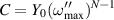
where Y0 represents the characteristic parameter of the CPE similar to capacitance,  the frequency which produces maximum −Zʹʹ, and N an additional CPE parameter, where N = 1 for an ideal capacitor.
As-deposited devices A and B were cross-sectioned for transmission electron microscopy (TEM) using a focused ion beam / scanning electron microscope (FIB/SEM, FEI Nova 600 NanoLab). The FIB/SEM allowed thin cross-sections ( ) to be lifted-out from the electrode pad region, ion-polished to be 100 nm thick ready for TEM imaging. All the preparation procedures were kept the same and mounted on the same TEM grid to allow direct comparison between the two cross-sections. TEM bright field images were recorded using a FEI Tecnai F20 field emission gun scanning transmission electron microscope (FEG-STEM).
X-ray photoelectron spectroscopy (XPS) of the Ag 3d and Si 2p levels was used to investigate Ag concentration in both samples. XPS was performed using a Thermo K-Alpha system with an Al Kα mono-chromated (1486.6 eV) source with an overall energy resolution of 350 meV.
3. Results and discussion
Resistive switching in each device was studied via analysis of dc I–V characteristics (figure 1). Device A (figure 1(a)) demonstrated switching behavior which can be described as analog, with a gradual conductivity increase towards I
 . Interestingly, current measured under increasing and decreasing voltage sweeps showed almost identical behavior with a negligible hysteresis. Such a property would suggest a non-linear differential resistance dependence on the applied voltage bias, with a negligible hysteresis. This is in contrast with conventional diffusive memristors, which typically demonstrate an observable hysteresis.

Figure 1. I–V characteristics for (a) device A and (b) device B, where black and red lines denote increasing and decreasing voltage, respectively. Insets show top-view optical microscopy photographs for both devices.
Download figure:
Standard image High-resolution imageDevice B, on the other hand, demonstrated a rather abrupt resistance switching (figure 1(b)) that is more conventional for diffusive memristors. There is a clear threshold voltage at V
 0.325 V at which current sharply increases to I
 , in contrast to the analog behavior exhibited by device A.
Devices A and B have electrodes consisting of different materials, Au and Pt, respectively, which have both been previously shown to display familiar resistive switching behavior in similar memristors [15, 42]. The relatively small deviation in the dielectric layer thickness values, 50 nm vs 40 nm, should not cause any significant difference in the switching behavior, either, based on the previous literature reports [43, 44]. XPS measurements revealed that the atomic concentration of Ag in the switching layers of both devices A and B were approximately 12.9 and 7.6
 , respectively. Hence, the major factors in defining the switching behavior in our samples appear to be either the Ag concentration [17, 45] or the electrode geometry and size [46].
TEM has been used to investigate the thin film layers of both devices (figures 2(a) and (b)), while also providing information about the scale, distribution and densities of Ag nanoparticles, represented by the darker color in the SiO :Ag switching layers. The switching layer of device A showed a less homogeneous distribution of Ag nanoparticles both spatially and in terms of the size, than device B. Ag can also be observed in the top Ti layer of device A, which can promote filament growth from the top electrode in this case. Typical nanoparticle size in device A ranges between 5 nm and 10 nm, compared to generally smaller nanoparticles in device B, though these do possess a similar range of 3 nm–10 nm in diameter. Qualitatively, device A (figure 2(a)) can be seen to have a larger concentration of Ag particles in its switching layer, in comparison to device B (figure 2(b)). This can be linked back to the XPS data, in which the Ag concentration was found to be higher in device A than device B.

Figure 2. Cross-sectional TEM images of (a) device A (b) device B. Ag nanoparticles of varying sizes can be observed in the switching layers of both memristors, which form conductive filaments between electrodes when in the LRS.
Download figure:
Standard image High-resolution imageThe top electrodes of both memristors can be seen to be relatively rough on their respective interface. Figures 2(a) and (b) suggest that formation of conductive filaments is guided by Ag nanoparticles situated by the top (positive) electrode surface. Based on the understanding of how diffusive memristors operate, both images represent the HRS of the corresponding devices. For the LRS, the Ag nanoparticles would fully bridge the gap between electrodes, making the devices conductive.
In order to investigate the impedance of both memristors whilst in the HRS, both devices were subject to multiple voltage biases, the values of which were chosen to remain below the switching threshold voltage ( ). At the same time, a lower limit was placed on
  values, below which the HRS resistance was too high to be measured through EIS. Figures 3(a) and (b) show the Nyquist plots for both devices after being exposed to varying
  . Both resistive and capacitive behavior is observed for both devices in their HRS, with the widths of the completed arcs decreasing with increasing voltage bias, indicating decreasing device resistance [23]. This is to be expected, as a diffusive memristor approaches its LRS with increasing applied voltage, allowing for a non-linear increase in leakage current to happen. This change in resistance is significantly more noticeable in device A (figure 3(a)) than in device B (figure 3(b)). While the arcs in figure 3(b) do decrease as voltage increases, the difference in width, and therefore device resistance, between subsequent measurements is less pronounced than the analog switching device. This behavior can be linked back to the I–V characteristics shown in figures 1(a) and (b), where device B displays a significantly smaller change in resistance before switching to the LRS.

Figure 3. Imaginary vs real components of the total impedance (Nyquist plots) measured in the frequency range 60 Hz–0.6 MHz for varying voltage bias across (a) device A and (b) device B, with the corresponding fits (red solid lines) produced by equivalent circuits. Insets show equivalent electrical circuits for both devices.
Download figure:
Standard image High-resolution imageThe insets of figures 3(a) and (b) show the equivalent circuits of each device which would produce the best fit to the experimental impedance spectra. A series resistor in either configuration translates a Nyquist plot along the x-axis by its corresponding resistance value [23], effectively estimating the high-frequency components of the spectrum [47] and can be attributed to the electrodes [26], while the parallel elements model the behavior in the switching layer and determine the width, height and curvature of the arcs observed in Nyquist plots such as figures 3(a) and (b). This is in a good agreement with previous studies, which demonstrated a comparable circuit for HRS of memristor devices in which no additional phases are expected in the switching layer [18, 20, 27, 31]. The switching layer in our case is represented by a parallel resistor-capacitor combination and produces a semicircular Nyquist plot fitting, as in figure 3(a), yielding a maximum  at frequency
  . This is not the case in figure 3(b), where the parallel capacitor is replaced by a CPE with N ≈ 0.95, a higher value than 0.8, which is typically found [48], suggesting near-ideal capacitance. While high, this value of N
 1 indicates non-ideal behavior could have been introduced by the increased roughness and inhomogeneity of the topmost Pt electrode layer [25, 49, 50], as visible in figure 2(b), where considerable roughness can be observed on the top electrode surface of device B. This is also an indication that a poorer short-range crystalline order is present in device B in comparison to device A, as the CPE is linked to a distribution of time constants [36]. This could be originating from the larger top electrode area of device B in comparison to device A. The equivalent circuits used to fit spectra for these devices do not contain inductance, as measurements were taken exclusively in the HRS in order to investigate the voltage dependence prior to switching. Once stable switching occurred in these devices, semicircular Nyquist plots were no longer observed, but replaced with values of
  , representative of a serial resistor–inductor connection, in line with previous literature [20, 27, 36]
For a single device, while these equivalent circuits remain consistent, the magnitudes of the circuit parameters are not necessarily constant for varying  , as shown in figure 4. In device A, resistance
  decreases rapidly with increasing
  , showing strong correlation with differential resistance values obtained by
  (red line in figure 4(a)), calculated from the I–V characteristics of figure 1(a). Device B shows a relatively lower decrease in resistance values obtained from EIS fits as well as slightly more of a contrast from the differential resistance calculated from I–V characteristics, albeit with similar trends, as portrayed in figure 4(b). Such a difference points to the increased stochasticity of device B, where a filament is formed swiftly with relatively little pre-forming, whereas device A apparently has an extended range of voltages at which intermediate filament precursor states are formed. At the same time, the relatively good agreement with
  values for both devices indicates that EIS is a reliable source of characterisation of the HRS in terms of the device resistance. The R
 values were constant in both cases and equal to 3.50 kΩ and 1.52 kΩ, on average, for devices A and B, respectively.

Figure 4. Device resistance,  , and equivalent capacitance, C, vs. voltage bias,
  , for device A (a) and (c) and device B (b) and (d) as obtained from fitting impedance spectra. For resistance curves (a) and (b) device resistance from equivalent circuits (black squares) are given alongside comparable differential resistances (
 ), plotted (red circles) as obtained from corresponding I–V characteristics.
Download figure:
Standard image High-resolution image
While both devices demonstrate capacitances of the same magnitude (pF), the CPE used in fits for device B (figure 4(d)) equates to higher capacitance values than the capacitors for device A (figure 4(c)), which in part could be due to the larger top electrode area for device B. Despite this, the two devices display a roughly consistent capacitance with increasing  , suggesting that capacitance is not strongly voltage-dependent when a device is in its HRS, prior to switching. On the other hand, the most notable difference in these plots is the increase in capacitance in device A at
  1 V, as the device in question approaches
  and thus its LRS. No such increase is observed for device B in terms of equivalent capacitance.
The equation for a plane capacitor  states that capacitance is proportional to the dielectric constant ε, the vacuum permittivity ε0 and the electrode area A, and inversely proportional to the distance, d, between plates, or electrodes in the case of these memristors. If one assumes the conductive filament between two metallic electrodes in a diffusive memristor to be an extension of the top electrode from which it grows, then capacitance will increase in line with filament growth due to the decrease in distance between electrodes. Such a scenario would only occur if a filament grows significantly in length without completely connecting the electrodes of a memristor, thus ensuring the device remains somewhat insulating. This case applies to bias values of 1.25 V and 1.50 V in figure 4(c), where device A approaches compliance current whilst not behaving completely metallically. Therefore, a significant increase in capacitance is observed for the analog switching device. In device B, one could also consider the more abrupt filament forming meaning the precursor filament state is forming less considerably whilst in the HRS. Furthermore, the switching layer in device A being thicker than that of device B (40 nm vs 50 nm) may be another factor that allows the aforementioned precursor filament to develop in device A without completely bridging the gap between the electrodes.
By developing the idea of a plane capacitor even further in relation to a diffusive memristor, one could speculate about certain areas within each device where the average distance between the electrodes is much less than the nominal film thickness, for example, due to a precursor filament state formation. By noting those areas having electrode area A0 and local distance d0 as capacitor thickness, compared to A and d as nominal electrode area and distance, respectively, the original plane capacitor formula would transform into ![$C = {\epsilon}_{0}{\epsilon}[(A-A_{0}) / d + (A_{0}/d_{0})]$](https://content.cld.iop.org/journals/0022-3727/56/30/305102/revision2/dacd06cieqn55.gif) which is approximately
which is approximately ![$C = \epsilon_{0}{\epsilon}[A / d + A_{0}/d_{0}]$](https://content.cld.iop.org/journals/0022-3727/56/30/305102/revision2/dacd06cieqn56.gif) if
if  d. In this scenario the capacitance could increase due to appearance of additional A0/d0 terms caused by one or several pre-filament states forming. Alternatively, impact of pre-cursor filament states on capacitance would be smaller than the one on the resistance if the precursor state is formed by a relatively small area A0, effectively making the additional term
  relatively small, whereas the corresponding non-linear resistance associated with this area would be significantly lowered in comparison to the rest of the device. In other words, the total resistance of parallel coupled resistors is dominated by its smallest resistance (i.e. those with d0), however the total capacitance of parallel capacitors is dominated by its largest part (i.e. the one with the nominal
  ). Such a phenomenon would explain the relatively modest increase in capacitance at higher
  observed in figures 4(c) and (d) in comparison to the relative resistance decrease observed in figures 4(a) and (b). The phenomenon of increasing C values in HRS, which seems to be similar to that reported in [37], is probably linked to the rearrangement of Ag ions prior to the complete formation of the switching filament. Rather more inhomogeneous Ag particle distribution in device A (figure 2(a)) appears to reduce the overall capacitance when the Ag particles are concentrated largely at the top electrode interface at lower bias voltage, however, the capacitance is increasing when Ag particles start to be field-driven into the dielectric matrix. At the same time, Ag nanoparticles present in the dielectric matrix of SiO
 do not create an additional arc representing a separate electric circuit element due to the interface, as was demonstrated in [32, 37].
4. Conclusion
In summary, two distinct diffusive memristors have been investigated through EIS, each demonstrating individual switching behavior and impedance spectra. This study represents, to the best of our knowledge, the first attempt to apply EIS to specifically characterize a volatile memristor with conductive filaments as a resistive switching mechanism. Through the analysis of the dependence of equivalent circuit parameters on the applied bias voltage, we illustrate, with supporting evidence of I–V characteristics and TEM cross-section images, how dominating switching mechanism and the equivalent electric circuit can be identified over a range of applied voltage bias values whilst a device remains in the HRS.
A single capacitor with a parallel leakage resistor was used to yield the best fit of Nyquist plots describing a single switching layer in HRS with no sizeable contributions due to a secondary layer or an interface. We observe a relative good correlation between the obtained  values for the analog device A and the differential resistance obtained from the I–V curves whilst the digital switching in device B shows a rather deviating behavior with less change in the HRS resistance. Similarly, the capacitance of device A, showing the analog switching, demonstrates a ∼25% increase closer to the threshold voltage whilst device B is rather stable in this regard. The inhomogeneous Ag particle distribution in device A and its consequent transformation with increasing voltage bias are assumed to be at the origin of this behavior. These results advocate for more active employment of EIS measurements for characterization of volatile memristive devices.
Acknowledgment
The authors would like to thank Sam Davis for the FIB and sample preparation prior to TEM, and acknowledge the use of the facilities within the Loughborough Materials Characterisation Centre. Additionally, we wish to thank Dr Christopher Mellor for his assistance in fabricating samples. The authors also wish to thank both Prof. Upul Wijayantha and Dr Michael Cropper for their experimental expertise and helpful discussion regarding material preparation and characterization. This work was supported by The Engineering and Physical Sciences Research Council (EPSRC), Grant No. EP/S032843/1.
Data availability statement
All data that support the findings of this study are included within the article (and any supplementary files).