
Abstract
Metal–graphene–metal (M–G–M) stacks have provided new specific methods for the integration of two-dimensional (2D) materials into three-dimensional (3D) electronic devices, such as transistors, supercapacitors, memristors and others. Intentional control of the local electronic properties in the stacks is the primary problem to be solved when developing hybrid structures with 2D and 3D elements. In order to do this, the physical mechanisms and processes that define the properties of the stacks must be thoroughly understood. This report introduces an approach based on the force curve analysis in terms of the interface characteristics in the M–G–M stack. In the study, the stack was produced by pressing the platinum probe of a scanning probe microscope into the surface of a gold-supported graphene monolayer, and the force curve was measured under applied direct current voltage. Based on the model of the van der Waals contact, the equilibrium interface distances and the built-in potential were obtained from the experimental results. The equilibrium state was proved to be weakly dependent on the applied voltage below a threshold level. Above this level, irreversible changes and the effect of the history of the tests were detected. The proposed method is acceptable to quantitatively describe the most essential characteristics in a local area of the M–G–M stack, essential for the construction of nano-scaled electronic devices.
Export citation and abstract BibTeX RIS

Original content from this work may be used under the terms of the Creative Commons Attribution 4.0 license. Any further distribution of this work must maintain attribution to the author(s) and the title of the work, journal citation and DOI.
1. Introduction
Interactions between graphene and supporting metal surfaces have been intensively analyzed in various theoretical and experimental studies with quite diverse objectives and approaches. Promising functional features were demonstrated at heterojunctions between two-dimensional (2D) and three-dimensional (3D) materials [1]. A large number of applied technology solutions have been presented, with the primary focus on the interface engineering of hybrid systems, including low-dimensional materials [2]. Some promising applications have been proposed, combining 2D layers with metal and semiconductor constructions [3]. However, it has been recognized that an improvement of the electrical contacts in graphene electronic devices requires a better understanding of physical mechanisms for controllable down-scaling of the devices in the integrated modules [4]. Therefore, there have been attempts to develop comprehensive physical models for detailed analysis of the graphene–metal contacts [5]. The models significantly improved understanding of the mechanisms controlling the crucial characteristics of the contacts. The adsorption is mainly associated with the van der Waals interaction, resulting in a hybrid heterojunction with built-in potential barrier, the height of which depends on the properties of the individual contacts [6]. First-principles calculations suggested that the metal–graphene interaction can be intentionally controlled by choosing the metal depending on the hybridized states created at the interfaces [7].
It was demonstrated that the adsorption distances and the structure of the metal surfaces can drastically change the graphene–gold contact [8]. Extensive experimental studies suggested the idea that the interface distances are crucial for the characteristics of the contacts [9]. However, it has been recognized that effective control of the contacts requires a comprehensive understanding of the charge transfer between the solid surfaces [10]. Localized graphene doping is one of the most essential physical effects that complicates the description of the interaction properties. On the other hand, this effect suggests highly attractive properties to control the electronic properties in the layered structures.
The effect of local doping in graphene was explicitly demonstrated by analysis of the polarization in the construction of 2D MgO flakes on graphene layers [11]. A localized topological defect role for electronic coupling at the graphene–metal interface was proven to be useful for graphene-based electronic device performance control [12]. A much more effective way to control the properties of graphene was demonstrated in constructions having a sandwich-like arrangement of layers. The doping of graphene was proved in metal–graphene–metal (M–G–M) sandwiches by density functional theory calculations [13]. Detailed investigations of the current–voltage (I–V) characteristics disclosed unique dependences of the electrical properties on the M–G–M parameters [14]. However, it was recognized that the sandwich-like geometry was quite challenging to first-principles transport calculations and required specific approaches as it proposed for the 'side-contact' geometry [15]. In spite of that, significantly simplified analytical models proved to be quite effective in the analysis of the electrical characteristics of metal–graphene interfaces in addition to the first-principles calculations [16]. These simplified models were highly useful for better understanding the physical picture in the relationship between the experimental and theoretical parameters. Accepting the idea of the possibility to modify the interface distances in the layered structures with graphene, it was reasonable to expect changes in the properties under a compressive force applied perpendicular to the surfaces of the layers. Such changes were theoretically predicted for heterostructures with graphene [17, 18]. Moreover, it was proved that strain engineering can be used to form graphene quantum dots (QDs) originating from nano-bubble objects and nano-scale p–n junctions [19, 20]. Even without direct QD formation, unexpected changes were related to the interlayer distances in the local electrical charge transfer studies in the M–G–M structures. Aiming to explain the highly specific results, the layout of the atoms in the adjacent layers was suggested as the primary cause for the variations in the interlayer distances [21]. The extraordinary relationship between the applied compressing force and the electrical current was explained by the Fermi level dependence with the force leading to specific changes in the tunneling current across the interface barrier [22]. The changes in the electrical charge distribution in such M–G–M systems change the electrostatic forces, which are part of an experimentally measured adhesion force [23]. Despite the highly intriguing results discussed in this brief overview, the theoretical description and relationship between the experiment and the theory is still quite a challenging problem. The experiments are typically complicated by the technological challenges of the sample production and limitations of the measurement methods in the nanoscale arrangements. Therefore, the present work was focused on the method based on the force curve measurement by atomic force microscopy (AFM) and an interpretation of the results in terms of the Fermi level, interface distance and electric charge redistribution at the interfaces.
In the present report, an M–G–M stack was produced by pressing the platinum probe of a scanning probe microscope (SPM) into the surface of a gold-supported graphene monolayer. The force curve was investigated under an external direct current (dc) voltage applied perpendicular to the M–G–M stack. The interaction between the graphene and the metal was analyzed as a van der Waals contact and the interface characteristics were related to the experimentally obtained built-in potential, distances between the contact surfaces and the probe parameters. The influence of the applied voltage on the shift of the Fermi level and the distances was revealed.
2. Experimental section
2.1. Sample structure and manufacturing
A key part of the tested samples was gold-supported monolayer graphene. For the supporting Au, a thin film was deposited by a dc magnetron sputtering method. The Au film thickness was about 100 nm and the root-mean-square (RMS) roughness less than 0.4 nm. The film was grown on a standard Si plate with an insulating SiO2 layer with a thickness of about dSiO2 = 275 nm. The samples were produced by wet transfer of a graphene layer on the surface of the Au film. A commercially available chemical vapor deposition (CVD) grown graphene monolayer (Graphenea) was used for this. The transfer method was described in detail in a previous study [24]. The substrate with the graphene was annealed in Ar atmosphere at 300 °C for 124 min before the investigation [22]. In this work, the complete samples consisted of the SiO2/Si substrate, supporting Au film, a graphene layer and a conductive probe as the top electrode.
The outline of the sample arrangement is illustrated in figure 1(a). In this figure, a schematic is also shown of the electrical measurements combined with the mechanical force curve ramps. The supporting Au film was used as the bottom electrode (M2), whereas the probe of an SPM was the top electrode (M1) in these experiments. The probe also produced a compressing force perpendicular to the surface of the layered structure. Accepting that the graphene was fixed by the van der Waals forces on the Au film, a schematic of the deformations under the compressing force is shown in figure 1(b). In this schematic, the tip of the Pt probe is represented by a ball with the diameter equal to the tip diameter. The interlayer distances due to van der Waals forces are indicated by dGM1 for the interlayer between the Pt probe (M1) and graphene (Gr) monolayer and by dGM2 for the interlayer distance between the graphene (Gr) and Au film (M2).
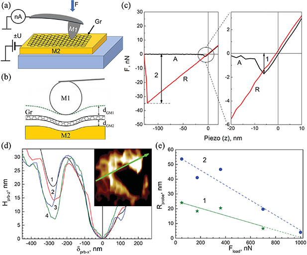
Figure 1. (a) Schematic of the sample and principles of the electrical and mechanical measurements. (b) Schematic of the deformations under probe compressing force. Reproduced from [22]. © IOP Publishing Ltd. All rights reserved. (c) Experimental force curve with the special points of the snap-in (1, right panel) and jump-off (2, left panel). (d) Cross-section of the tip of an SPM Pt probe obtained from the reconstruction experiments with the probe compressing forces: 49 nN (1), 173 nN (2), 360 nN (3) and 700 nN (4). Inset: flat representation of the tip contact obtained from the reconstruction experiments. The cross-section corresponds to the arrow. Reproduced from [22]. © IOP Publishing Ltd. All rights reserved. (e) The tip radius Rprobe versus the compressing force Fload of the probe at the height Hprb-z 0.3 nm (1) and 1 nm (2) in the cross-section in (d).
Download figure:
Standard image High-resolution image2.2. Measurement methods
The force curves were measured using a Dimension 3100 SPM (Veeco Inc.). For this, the force was sequentially changed by pressing the probe into the surface in the approach and retract paths. A typical force curve is illustrated in figure 1(c) by the dependence of the tip–surface interaction force F on the height z equal to the length change of the piezoceramic driver. In the approach path, switching is typically detected for the probe when the non-contact state changes to the contact state for the tip of the probe. The switching corresponds to the height when the long-distance attraction forces exceed the deformation force of the cantilever. At this point, the snap-in force Fsnap was measured at the apex of the triangle in the approach curve (figure 1(c)–A, right panel). When the probe was moved back from the surfaces, the tip was in contact with the surface until the deformation of the cantilever exceeded the adhesion forces. The adhesion forces Fadh were measured at the apex of the triangle in the path of the retract probe (figure 1(c)–R, left panel). The maximum compressing force was about Fmax ∼ 190 nN at the maximal indentation in the surface. The SPM probe force was calibrated by measuring the force–distance curve on a hard clean surface (reference platinum grating sample (Bruker)) in contact mode. From a linear part of the curve, the cantilever deflection in nanometers was found, and using the nominal value of the cantilever spring constant k, the numerical force value F was calculated by Hooke's law [25].
The tunneling atomic force microscopy (TUNA, Veeco Inc.) module was connected to the SPM for the electrical measurements. An external constant dc voltage Vapp was applied between the probe and the Au film by the TUNA during each force curve measurement. Between two sequential measurements, Vapp was changed in a stepwise manner so that an individual pattern of the voltage sequences could be associated with a specific sequence of voltages collected from the interval −1.5 V ⩽ Vapp ⩽ + 1.5 V. In these experiments, a pure Pt probe (Pt-rock, model RMN-12Pt400B, Bruker) was used as the base potential electrode. The geometry and dimensions of this probe-based electrode were described by a physical image of the probe end obtained from a special reconstruction experiment.
A commercial TipCheck (Budget Sensors) reference plate was used for probe tip reconstruction. The reconstruction of the tip was performed according to the proposed method [26]. The TipCheck plate surface covered by an intentionally produced rough layer was scanned by the probe pressed into the surface by a fixed force. The AFM topography images were analyzed by a tip characterization module in the commercial data processing software package scanning probe image processor (SPIP, Image metrology A/S). As a result, the probe tip was visualized by a 3D image acceptable for measurement of the dimensions. Typical characteristics of the probe tip are illustrated in figure 1(d) by the profile lines of the cross-sections obtained at four individual compressing forces Fload. In the inset, a flat representation of the tip image is visualized. The cross-section was obtained along the arrow in the inset in figure 1(d). According to the methodology [24], the accuracy of the tip visualization depends on Fload. For a comparably small Fload, the interaction between the tip and the sample surface is weak, and the accuracy of the topography measurement is low. Increasing the Fload increases the accuracy of the measurement. It is worth noting that the additional rock of the tip can be seen in figure 1(d). For the forces used in our experiments, this additional rock was 7–20 nm above the main rock of the tip and therefore did not have any influence on the experimental results. The accuracy of the visualization is illustrated by the dependences of the radius of the tip Rprobe versus the compressing force Fload shown in figure 1(e). The radius was obtained from the cross-section in figure 1(d) by measuring the width of the tip at a fixed height Hprb-z from the apex of the tip. The dependences in figure 1(e) are presented for two heights Hprb-z equal to 0.3 nm and 1 nm from the apex. These results were used to model the long-range force interaction between the probe and the surface.
More details on the methodology of the investigation of the mechanical and electrical properties in an M–G–M vertical structure were presented in a previous work [22].
3. Results
The most important limiting condition in this study was the distance between the probe and the surface defined by the contact mode in SPM investigations. In this case, the tip of the probe was a flat metal electrode on the surface of the monolayer graphene. This condition is fulfilled when the distance between the graphene surface and the tip (dGM1) is much smaller than the radius of the tip rock (Rtip). According to the experimental results, Rtip is in the range of 5–55 nm under various load forces, whereas dGM1 is typically in the range of a few angstroms. The simplification of the geometry of the tip of the Pt probe was justified for tip–graphene distances lower than the tip radius dGM1 ≪ Rtip. Under this condition, the construction Metal1–Graphene–Metal2 (Pt probe–monolayer graphene–thin Au film) was investigated on the basis of a flat capacitor model. The results of the investigation included the output of the numerical model analysis, the experimental force curves measured with applied external voltage and the model-to-experiment fitting parameters with the physical meaning in the experiments.
3.1. Model description and fitting parameters
Accepting dGM1 ≪ Rtip in the model, three mechanisms of the interaction forces between the components were included. First, in the classical approach, the electrostatic force between an SPM probe and the conductive surface is typically described as the force between the electrodes in a flat capacitor FC. Second, at very short distances (<1 nm) a redistribution of electrons cannot be neglected in a metal–graphene system. The extra doping of the graphene results in a short-range force FtQ in the interaction between the probe and the surface. Third, microcapillary and van der Waals-originated forces Fsurf are typically detected due to surface molecular water and technology built-in material features in the SPM experiments. Assuming acceptable the sum of the independent components, the probe–surface interaction can be described by the total force

Due to the mechanisms of the interaction, the first two terms FC and FtQ in (1) are dependent on the applied external voltage V.
The force FC between the electrodes in the plane parallel capacitor can be described by the simple relationship
where C is the capacitance of the capacitor, Rtip is the Pt probe radius, LC is the distance between the M1 and M2 electrodes and  gap is the dielectric permittivity of the substance in the capacitor. In equilibrium, it can be written

where dMGM is the total thickness of the M–G–M system, and dGM1 and dGM2 are the interface distances between the graphene sheet and the top (Pt) and bottom (Au) electrodes, respectively.
The force FtQ between the Pt probe and the electric charge Q originated from the extra charge in the graphene due to the electrons being transferred between the graphene and the probe. The charge was quantitatively determined by the relative density of the transferred electrons NgQ for the unit cell of graphene. The force FtQ can be described by a model based on an electric charge Q in a homogeneous electric field E produced between the electrodes by an external dc voltage. It can be obtained by a simple description:
where the graphene unit cell volume σcell = 5.18 Å2, and e is the electron charge.
The third force term in equation (1), Fsurf, is accepted as a constant force component producing a shift of the base signal independent of the applied voltage in an individual force curve measurement cycle. As the Fsurf term, by our definition, contains van der Waals-originated forces, all voltage-dependent force components are included in the first and second terms of equation (1), while the components in the third term are voltage-independent.
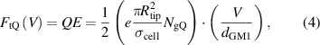
It follows from equations (2) and (4) that the force terms FC and FtQ are related to the parameters dMG1, dMG2 and NgQ that are the characteristics of the interface properties in the M–G–M system. These parameters can be calculated for the M–G–M system in the equilibrium state by the model proposed initially in earlier work and successively adapted to M–G–M systems in a recent work [16, 22]. The phenomenological version of the model was used to perform a quantitative comparison between the model and the experiments. It must be noted here that the acceptability of the model was limited to the weak interaction between graphene and metal layers that was valid for Au and Pt in this work. There was also another model limitation on the energy interval defined by ±1 eV from the Dirac point, within which the Fermi level shift can be digitally analyzed assuming linear dependence of the density of the electronic states. This restriction was acceptable here in the force model analysis because the compression force produced a lower shift in the Fermi level as it was proved for the flat construction of the M–G–M system [22]. The Fermi level shift ΔEF-eq-MGM important for the present study is illustrated in figure 2(a) by a dependence on the total thickness dMGM of the M–G–M system in equilibrium. The numerical results of the model analysis were obtained assuming a balance between the components of the M–G–M system defined by the same Fermi level across a stack of flat layers. Therefore, the results in figure 2(a) can be understood as a visualized set of the related parameters (ΔEF-eq-MGM, dMGM) defining the equilibrium state in the M–G–M flat layer stack. It follows from these results that the shift was within the limitation |ΔEF-eq-MGM| < 1 eV if the M–G–M stack was thicker than about dMGM > 5.1 Å. In addition, the equilibrium state limited splitting into the related interface thicknesses dMGM= dGM1 + dGM2 is graphically presented in figure 2(a) as the dependences of the split components dGM1 and dGM2 versus dMGM. The changes in the M–G–M system due to the applied dc voltage Vapp were obtained by modifying the model from previous work and including Vapp in the relationship:

Figure 2. (a) Model calculation of the metal–graphene distance (dGM1 and dGM2) and the Fermi level shift (ΔEF-eq-MGM) versus total thickness dMGM of the stack M–G–M at equilibrium defined by the equality of the Fermi level through the flat M–G–M stack. (b) Influence of an increase in external voltage on the number of electrons (per unit cell) transferred from the metal to graphene (negative) and vice versa (positive) at the interfaces graphene–Pt (1) and graphene–Au (2) with dGM1 = 2.88 nm and dGM2 = 3.14 nm.
Download figure:
Standard image High-resolution imagewhere WM and WG are the work functions of the metal and graphene, respectively, and ΔVC is the barrier height in the metal–graphene contact [16]. Accepting equation (5), the model characteristics were calculated in the interval of the voltages −1.5 V ⩽ Vapp ⩽ + 1.5 V. The results of the numerical analysis of the M–G–M system are graphically illustrated by typical dependences in figure 2(b). In the graphics, the amount of electrons NgQ transferred to (NgQ < 0) and from (NgQ > 0) graphene are plotted as a function of Vapp for the both graphene–metal contacts under the equilibrium condition of an identical Fermi level in the entire M–G–M stack. The dependences of NgQ on Vapp were sensitive to the changes in the equilibrium distance dMGM and, consequently, these changes were reliably detected in the interaction force Fadh obtained from the numerical simulation of the model described by equations (1)–(4). The sensitivity of Fadh on the graphene–metal distance dGM2 is illustrated in figure 3(a).
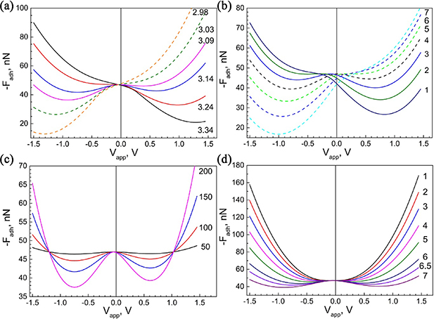
Figure 3. Model calculation of the tip–surface interaction force versus applied electrical voltage at the M–G–M system equilibrium defined by the equality of the Fermi level in the entire system under specific conditions: (a) with individual graphene–gold interface distance dGM2 (Å), (b) with diverse intrinsic voltage shift VS (mV) = −300 + 100(n − 1) (n is numeric label), (c) for diverse radius of the tip Rtip (Å), (d) changes in the dielectric permittivity in the gap between the tip and the sample gold electrode gap. Only one parameter was changed in each individual set of dependences. The set of parameters dGM2 = 3.14 A; VS = − 0.045 V; Rtip = 15 nm; gap = 6.5 was used as the reference model calculation.
Download figure:
Standard image High-resolution imageIn figure 3(a) the dependence of the adhesion force Fadh on the applied voltage Vapp is graphically plotted for diverse fixed distances from the interval 2.98 Å ⩽ dGM2 ⩽ 3.34 Å. It is helpful to note here that a reference M–G–M system was introduced for the detection of the changes in Fadh vs. Vapp produced by a change in the selected parameters. The reference system was described by a set of numerical values of the parameters: dGM2= 3.14 Å, Rtip= 150.0 Å, gap= 6.5, Fsurf= 47.0 nN, VS= −45.0 mV (table 1). The parameter VS was interpreted as an additional voltage shift (V= Vapp + VS) originating from uncontrolled extra electrical charges related to doping, irreversible changes and similar non-predictable effects in the system. It is useful to mention that this reference set of parameters led to model forces quantitatively close to the measured forces, with similar essential features of the dependence Fadh vs. Vapp. Although the details of fitting the model to the experiment are presented below in this text, here the reference set was used to compare the influence of the adjustable parameters on the results of the model calculations presented in figure 3.
Table 1. Parameters used for fitting the model calculations to the experiment. Graphene–Pt distance dGM1, graphene–Au distance dGM2, effective tip radius Rtip, dielectric permittivity of the interface gap gap, extra force due to the surrounding influence on the tip Fsurf, and internal extra potential difference VS.
| Identity | dGM1 (Å) | dGM2 (Å) | Rtip (Å) |
gap (a.u.) | VS (mV) | Fsurf (nN) |
|---|---|---|---|---|---|---|
| Figure (3) Reference | 2.88 | 3.14 | 150.0 | 6.5 | −45.0 | 34.0 |
| Figure 4(a)-1 | 3.00 | 3.34 | 150.0 | 6.5 | 300.0 | 38.0 |
| Figure 4(a)-2(ref) | 2.88 | 3.14 | 150.0 | 6.5 | −45.0 | 38.0 |
| Figure 4(a)-3 | 2.91 | 3.19 | 200.0 | 6.5 | 35.0 | 40.7 |
| Figure 4(b)-1 | 2.91 | 3.19 | 200.0 | 6.5 | 35.0 | 53.0 |
| Figure 4(b)-2(ref) | 2.88 | 3.14 | 150.0 | 6.5 | −45.0 | 49.0 |
| Figure 4(d)-1 | 2.91 | 3.19 | 55.0 | 1.0 | 0.0 | −1.15 |
| Figure 4(d)-2 | 2.91 | 3.19 | 60.0 | 1.0 | 0.0 | −1.45 |
| Figure 4(d)-3 | 2.91 | 3.19 | 25.0 | 1.0 | 0.0 | −1.0 |
| Figure 4(d)-4 | 2.91 | 3.19 | 200.0 | 1.0 | 0.0 | −1.0 |
It can be understood from the comparison of the model calculations for diverse dGM2 with that for the reference system in figure 3(a) that a wave-like variation in Fadh vs. Vapp is highly sensitive to the changes in the interface distances. This wave-like variation was practically suppressed by a higher than ±6% deviation from the reference system. In addition, an asymmetric form of the dependence was obtained with respect to V= 0. Unexpectedly, the voltage shift VS produced completely the opposite effect on the dependence Fadh vs. Vapp compared to that in figure 3(a). The VS effect is illustrated in figure 3(b) by a set of calculated dependences Fadh vs. Vapp for the model with individual voltage shift from the interval −300 mV ⩽ VS ⩽ 300 mV.
According to the results of the model simulation in figure 3(c), the sensitivity of the force detection can be significantly increased with an increase in the tip radius from 50 Å to 200 Å. In contrast to that, the force originating from the electrostatic interaction mechanism was noticeably reduced with the increase in dielectric permittivity gap of the substance between the metal electrodes, as demonstrated by the model calculations graphically presented in figure 3(d). The plotted dependences Fadh vs. Vapp were obtained, accepting individual permittivity from the interval 1.0 ⩽ gap ⩽ 7.0 for the M–G–M stack in the model calculations.
3.2. Extraction of the interface characteristics from the force curves
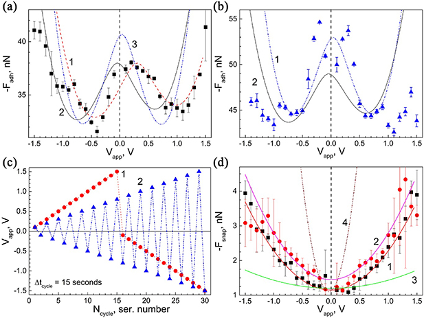
The retrace part of the force curve is directly dependent on the properties of the hard contact between the tip and the surface. Therefore, the pull-off triangle in the SPM force curve (figure 1(c)) was experimentally studied for quantitative analysis of the interaction between the components in the M–G–M system. The force at the triangular apex Fadh was obtained from the measurements with voltage Vapp applied between the probe and the graphene-supporting Au film. Typical experimental dependences of Fadh on Vapp are graphically presented by the points in figures 4(a) and (b). In the figures, each individual point was detected under constant Vapp in an individual force curve cycle of 15 s duration. In order to produce the dependences on the voltage, Vapp was changed stepwise between the cycles according to the special algorithms. Two algorithms are graphically presented in figure 4(c). First, the magnitude Vapp was increased linearly for positive (0 → + |Vmax|) and then negative (0 → − |Vmax|) voltages (1 in figure 4(c)). Second, Vapp was increased like a zigzag path by switching the polarity from positive to negative for the same magnitude and back to positive in the next Vapp rise step (2 in figure 4(c)). It was set to |Vmax| = 1.5 V in all the experiments. For both algorithms of the voltage increase, the general shape of the experimental dependences Fadh vs. Vapp was similar to a wave-like form variation of Fadh with Vapp as in the model dependences in figure 3. The model dependences fitted to the experiment are also graphically presented by the corresponding lines with label 1 in figures 4(a) and (b), respectively. The numerical values of the tuned parameters are listed in table 1. For comparison, the reference model dependences are also presented by lines labeled with the number 2 in figures 4(a) and (b). Line 3 in figure 4(a) shows the similarity between the results corresponding to the individual algorithm of the Vapp increase in figure 4(c). It must be noted here that the parameter Fsurf was freely used to shift the dependences vertically without noticeable distortion of the key features. The numerical values of all the parameters can be compared for the plotted model dependences in table 1.
Figure 4. (a) and (b) Dependence of the tip–surface interaction force Fadh at the jump-off triangle apex in the SPM force curve on external applied constant dc voltage Vapp: experiment (points) and model calculations (lines). (c) Sequences 1 and 2 of a stepwise increase in the magnitude of Vapp with increasing serial number of the force curve cycle in consecutive measurements of the adhesion forces in (a) and (b), respectively. Vapp was constant during each individual cycle of the force curve measurement with duration Δtcycle= 15 s. (d) The snap-in triangle apex force Fsnap in the AFM force curve versus Vapp is the same as in (c) and (d): experiment (points) and model calculations (lines).
Download figure:
Standard image High-resolution image
The part of the force curve obtained during the approach of the probe to the surface was also analyzed using the same model as in equation (1). In this part, there was no contact between the tip and the surface, and only the long length forces were important. Consequently, the term FtQ can be excluded from equation (1). The results of the experiments and the model simulation are illustrated in figure 4(d). The experimental results (points in figure 4(d)) are presented by the force Fsnap detected at the apex of the snap-in triangle of the force curve. The dependences of Fsnap on Vapp were obtained using the same algorithms for the Vapp increase sequences as in figure 4(c). The lines in figure 4(d) were calculated from the model in equation (1) without FtQ. A parabola-like curve was used to describe the dependences of Fsnap on Vapp in figure 4(d). The model was fitted with the experiment for the set of parameters listed in table 1. It was quite complicated to identify the differences between the experiments with individual algorithms of the applied voltage by fitting the model with the experiment within the measurement errors. A comparison of the two sets of parameters in table 1 quantitatively describes the sensitivity of the model to the intentional changes in the tuned parameters. It is practically impossible to distinguish between the model dependences calculated for 50 Å ⩽ Rtip ⩽ 60 Å (lines 1 and 2 in figure 4(d)). The lowest part of the tip Rtip = 25 Å was clearly too small to result in the snap-in forces at higher applied voltages (line 3 in figure 4(d)). On the other hand, the snap-in forces were obviously too low for the probe Rtip = 200 Å (line 4 in figure 4(d)) that, on the contrary, fitted the model calculations of the pull-off forces in figures 4(a) and (b) well. It is worth noting here that some discrepancies between the experimental results corresponding to the individual algorithms were detectable on the basis of the model comparison with the experiment. However, the influence of the measurement history on the interaction forces was much less detectable in the M–G–M stack in figure 4(d) than in figures 4(a) and (b).
4. Discussions
A simple model of the interaction between an SPM conductive probe and the surface of graphene supported by a metal layer was quite acceptable for a description of the experimental dependences of the adhesion force on an applied voltage. The model-based analysis of the experiments proved that the SPM force curve was sufficiently sensitive to the arrangement of the interfaces in the system with the metal-supported graphene monolayer. The origin of the sensitivity can be understood to be due to the fact that a hard contact between the metal and graphene surfaces produces a redistribution of the electrons in the M–G–M stack. The electrical properties and the electrostatic interaction in the M–G–M stack are highly dependent on the distribution of the charge on the surfaces and at the interfaces. A compression force applied to the surface of the M–G–M stack modified the redistribution, as demonstrated recently by an investigation of electron transport across the stack [22]. The self-arranged double-charge layers resulted in attraction and repulsion forces as suggested [16]. Consequently, the probe tip was under an electrostatic force originating from the double-charge interface layers in the compressed M–G–M stack. The interaction was almost unchanged in the retrace path due to the sufficiently soft cantilever. Therefore, the cantilever deformation force was equal to the electrostatic interaction force in the M–G–M stack at the pull-off triangle apex. Since an applied electric voltage changes the charge redistribution, as proved in other works, the adhesion force was also modified in the M–G–M stack [14, 16]. The same mechanism can be used to explain the sensitivity of the interaction force to the intrinsic potential shift VS. Since the shift depended on the initial properties of graphene and the stack, these technologically controlled properties of the tested system can be quantitatively described by the shift voltage obtained from the SPM force curve investigation. The shift potential must also be sensitive to the defects in the graphene monolayer and is acceptable for the analysis of homogeneity of graphene sheets and the contact at local points in the M–G–M stack. The specific aspect of the arrangement of the interfaces in the stack can quantitatively be associated with the effective dielectric permittivity gap. In spite of the fact that the interface between metal and graphene can hardly be understood as a substance-filled space, the sensitivity of the parameter to the arrangement of the interfaces in the M–G–M stack suggested analogous interpretation with material between the electrodes of a capacitor. It can be assumed that the gap is acceptable for quantitative detection of the redistribution of the electric charge related to the technology and material properties in the M–G–M stack.
The model analysis in figure 3 demonstrated that the detection of the changes in the adhesion forces can be increased by increasing the radius of the probe tip Rtip. However, the model fitting with the experiment suggested the idea that the same tip characterized the local areas with diverse dimensions depending on the experimental details. It was obtained that Rtip ≈ 200.0 Å from Fadh vs. Vapp in figures 4(a) and (b), whereas the snap-in force Fsnap vs. Vapp analysis from the experiments for the same tip and stack in figure 4(d) led to a tip radius of Rtip ≈ 50.0 Å. Based on the probe tip description in figure 1(d), it can be assumed that only the lowest part of the probe is important in the interaction with the graphene surface before the hard contact is made. At this stage, the gap between the probe metal and the graphene surface can be reliably accepted as an air gap between the electrodes. After increasing the compressing force up to about 130–190 nN, a hard contact was produced, resulting in the charge redistribution. The charge transfer was possible between the deformed graphene surface and the probe points at greater distances from the tip apex, as can be understood from figure 1(b). The tip image and the quantitative description of the probe end in figures 1(d) and (e) illustrates dependences of the effective area of the tip on the load force and the height of the probe that was 'visible' for the tested processes under individual measurement conditions. Therefore, the effective tip radius was accepted as a variable parameter for the fitting of the model with the experiments, despite the fact that the actual tip radius remained unchanged before and after the measurements. This dependence explains the differences in the radii in the experiments in the no-contact and the hard-contact regimes. Therefore, it is understandable that there was a significant difference in the radius of the same tip obtained from the Fadh and Fsnap experimental data.
It was worth noting here that a significant shift in the interface distances was detected from the comparison of the experiments performed according to individual algorithms of applied voltage increase in figures 4(a) and (b). The metal–graphene gaps dGM1 and dGM2 were larger (see table 1) if the absolute magnitude of only positive (negative) voltages was increased linearly up to the maximum compared to that of the zigzag positive–negative sequence in the M–G–M stack. The shift to the larger gap was mostly related to the voltages Vapp > 0.5 V (positive with respect to the supporting Au layer), whereas an opposite shift was detected for Vapp < −0.8 V. For the zigzag algorithm, the discrepancies between the model and the experiment were obvious for both polarities of the applied voltages if |Vapp| > 0.8 V. Since the changes in the interaction forces were practically irreversible for the higher applied voltages, it can be reasonably assumed that an external electric field switched the interface parameters into a new state, represented by the corresponding gap distances dGM1 and dGM2 and the Fermi level shift ΔEF. In spite of the irreversible changes in the measured electrical and mechanical parameters of the system in the interval of the high voltage, there was no physical damage detected in the graphene layer, as was shown experimentally [20, 22].
5. Conclusions
A simple model was proposed for a quantitative description of the adhesion force measured by an SPM in an M–G–M system. Based on the model, the experimental data were related to the characteristic parameters of the interfaces in the M–G–M stack. The model was verified by calculating the characteristic parameters from the experimental data obtained for the stack, which was produced by pressing a Pt probe into the surface of a gold-supported graphene monolayer.
The results of the study proved that the pull-off force detected in the SPM force curve was highly sensitive to the changes in the interface distances in the M–G–M stack. Assuming that the self-arranged stack equilibrium state was controlled by a constant probe compression force, the applied voltage was accepted to be the primary factor for the changes in the Fermi level shift, the related distribution of the electric charges and the resulting electrostatic forces of the interaction between the surfaces in the M–G–M stack with applied voltage. The set of model parameters specifically characterized the equilibrium state and the mechanisms of the changes produced by the applied voltage in the M–G–M stack. The assumption of a constant length of the M–G–M stack was verified by the model fitting with the experiment for comparatively low applied voltages in the interval from about −0.8 V to about 0.8 V. It was concluded that for higher magnitudes of applied voltage, the redistribution of the electric charge is correlated with the changes in the distances of the interfaces in the M–G–M stack. It follows from this analysis that there are two important conditions for the effect of applied voltage on the interface distances. First, there are threshold voltages limiting the acceptability of the idea of the rigid structure and constant interface distances. Above the threshold level, the geometry of the stack can be modified by the applied voltage. Second, the history of variation of the applied voltages must be analyzed in detail if the applied voltages exceed the threshold level, at least at some stages of the experiments. The effect of the history of the applied voltages will be analyzed in detail in our next study.
The local area of the changes in the M–G–M stack was extremely dependent on the contact distance between the conductive probe and the graphene surface. The area of the touching probe defined by the snap-in force curve point and the corresponding area of modified graphene was fourfold smaller than that of the probe forced into the hard contact. The difference can be explained by the changes in the repulsion force at very short distances in the model. The relative dielectric permittivity was proposed as an acceptable parameter to quantitatively characterize the polarization of charges at the interfaces in the M–G–M stack and the resulting interface interaction forces.
Based on the SPM force curves, a potential shift was introduced as a built-in interface potential difference originating from the mechanical deformations in the M–G–M stack. The potential shift can be modified by the applied voltage under specific conditions defined by the model.
The proposed method of the SPM force curve-based analysis of the interfaces in the M–G–M and analogous stacks still needs improvements because of the limitations related to the simplifications in the model description. Considering the very short distances, flat electrodes with a graphene monolayer were assumed to be acceptable for gold-supported graphene under a compressing force applied perpendicular to the surfaces by an SPM Pt probe. The geometry of the stack can be characterized more realistically using the description of the probe tip frequently used in AFM probe models. In addition, the forces originating from the polarized dipoles can be explicitly included in the model of the M–G–M stack. In spite of the possible improvements, it can be concluded that this simple model is still acceptable to describe the most essential features of the stack under external voltage. It is expected that the model analysis will be helpful for a better understanding of the physical nature of the mechanisms controlling the electrical charge transport in the channels that are perpendicular to the stacks with graphene and the layers of the 2D materials.
Data availability statement
All data that support the findings of this study are included within the article (and any supplementary files).