
Abstract
Two-dimensional (2D) materials have received extensive attention in optoelectronics because of their unique characteristics. However, due to the extremely thin thickness of 2D materials, their optical absorption is limited. In recent years, researchers have used different effects and structures to enhance the optical absorption of 2D materials. The waveguide, as a device to guide and limit light propagation, has been integrated into photodetectors based on 2D materials, most of which have been applied in the infrared spectrum. This article reviews the development of waveguide-integrated photodetectors based on 2D materials, mainly in the infrared spectrum in recent years. Discussions mainly focus on the preparation of materials in waveguide-integrated photodetectors, the design and simulation of waveguide structures, and the summary of research results and applications of waveguide-integrated photodetectors in recent years. Finally, the challenges and prospects of waveguide-integrated photodetectors are put forward and discussed.
Export citation and abstract BibTeX RIS

Original content from this work may be used under the terms of the Creative Commons Attribution 4.0 license. Any further distribution of this work must maintain attribution to the author(s) and the title of the work, journal citation and DOI.
1. Introduction
Photodetectors are devices for detecting and converting the light signal into an electric signal. Nowadays, photodetectors are attracting increasing interest in a wide range of applications, including sensing, environmental monitoring, communication, signal processing, and life science studies [1, 2].
Through the spectral range of detection, photodetectors can be divided according to their applicable spectral range, from ultraviolet to infrared spectrum. The infrared region can be subdivided into short wave infrared region, mid wave infrared region, long wave infrared region, and very long wave infrared region. Photodetectors used in infrared spectrum are widely applied in the following areas: remote sensing, intelligent medical treatment, and military. In the past decades, large amounts of materials have been used to prepare infrared photodetectors, including InGaAs, HgCdTe, InAs, and Ge. However, these materials have some disadvantages, such as lattice mismatch, complex manufacturing process, difficulty in integrating with complementary metal-oxide-semiconductor (COMS) devices (lattice mismatch with Si), toxic, and high cost [3–5].
In the meantime, with the discovery and application of two-dimensional (2D) materials in optoelectronic devices, more and more infrared photodetectors based on 2D materials have been prepared through different technologies and obtained fascinating performance [6]. Since graphene was successfully exfoliated for the first time in 2004, 2D layered materials have attracted more and more attention in the past decade due to their unique structural, mechanical, and physical properties for their atomic thickness. 2D materials refer to a type of material composed of layered atoms bonded by van der Waals' force. This weak interaction makes it easy to peel a few layers or even a single layer of material directly from the bulk material. The large family of 2D materials consists of graphene, black phosphorus (BP), hexagonal boron nitride, transition metal dichalcogenides (TMDCs), etc. Compared with bulk form, layered 2D materials show different properties [7]. For example, the bandgaps of typical TMDCs are tunable when the bulk crystal thins to monolayer, while researchers found that the bandgap of BP can be changed from 1.5 to 0.3 eV by adjusting the layers of BP crystal [8]. These adjustable band gaps enable researchers to make photodetectors suitable for different wavelengths in photodetection. In addition, due to their nano thickness, a part of 2D materials own high carrier mobility, such as graphene (130 000 cm2 V−1 s−1) [9], BP (∼1000 cm2 V−1 s−1) [10], and Bi2O2Se (>20 000 cm2 V−1 s−1) [11]. High mobility is of great significance for photodetectors, especially in response speed [12]. Besides, 2D materials have excellent mechanical flexibility. In recent years, flexible photodetectors based on 2D materials have made great progress in preparation and integration [13].
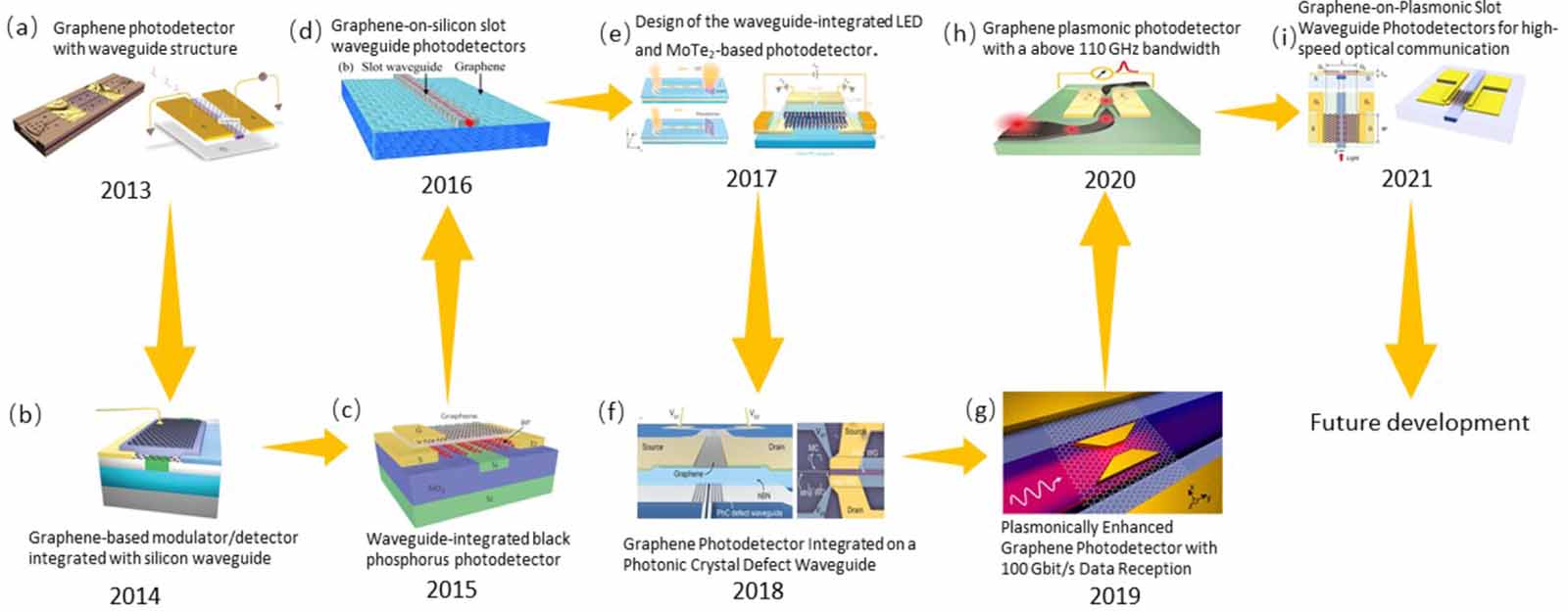
Although 2D materials show strong light-material interaction, the optical absorption is limited due to the atomic layer thickness of 2D materials. Xie, C summarized methods to enhance the interaction between light and materials including plasmonic nanostructures, optical waveguides, and optical microcavities [1]. Optical waveguides are devices that confine light to their interior or near surfaces and guide light to propagate along a certain direction, which can be divided into planar waveguides, slot waveguides and ridge waveguides according to their structure. Optical waveguides can be used to fabricate devices, such as lasers [14, 15], transistors [16], modulators [17], couplers [18], etc. In recent years, researchers have realized the combination of optical waveguides and photodetectors which can improve the performance of photodetectors. Since 2013, waveguide-integrated photodetectors based on 2D materials have achieved attractive detection achievements, as shown in figure 1. In 2013, Wang et al reported a graphene/silicon-heterostructure waveguide-integrated photodetector which firstly shows high responsivity (0.13 A W−1) in the mid-infrared range, as shown in figure 1(a). They also discovered two mechanisms for optical absorption which led to photocurrent dependence on bias polarity. In 2014, device based on graphene which has the functions of modulator and waveguide-integrated photodetector was demonstrated for the first time, as shown in figure 1(b). Such design proved that functions of multiple optoelectronic devices can be integrated in a single device. In 2015, another 2D material BP was also applied in waveguide-integrated photodetectors. The schematics of the structures are presented in figure 1(c). Compared with graphene, BP has the advantages of low dark current, high responsivity and quantum efficiency. Since then, different waveguide and integrated structures have also been applied to waveguide-integrated photodetectors, which continuously improves the performance and integration degree of waveguide-integrated photodetectors. In 2016, slot waveguide structure was demonstrated in waveguide-integrated photodetectors, which has a higher responsivity and more compact structure compared with traditional channel waveguides, as presented in figure 1(d). Besides, as the photonic crystal defect waveguide applied in 2018, responsivity was further improved, as shown in figure 1(f). In terms of integration, the researchers showed an example of the combination of LED light source and photodetector, as depicted in figure 1(e). Waveguide-integrated photodetectors also play an important role in high-speed optical communication. In recent years, waveguide-integrated photodetectors with high-speed capabilities (figures 1(g) and (i)), fast frequency response (figure 1(h)) has been demonstrated.

Figure 1. Timeline of waveguide-integrated photodetectors. (a) Two graphene photodetectors based on silicon waveguides [19, 20]. 2013, Copyright © 2013, Nature Publishing Group. (b) Graphene-based modulator/detector integrated with silicon waveguide [21]. 2014, © 2014 Optical Society of America. (c) Waveguide-integrated BP photodetector [22]. 2015, © 2015 Macmillan Publishers Limited. All rights reserved. (d) Slot waveguide integrated in graphene photodetector [23]. 2016, © The Royal Society of Chemistry 2016. (e) Design of the waveguide-integrated LED (light emitting diode) and MoTe2-based photodetector [24]. 2017, © 2017 Macmillan Publishers Limited, part of Springer Nature. All rights reserved. (f) Graphene photodetector with photonic crystal defect waveguide [25]. 2018, Copyright © 2018 American Chemical Society. (g) Plasmonically enhanced graphene photodetector [26]. © 2018 American Chemical Society. (h) Graphene plasmonic photodetector with bandwidth above 110 GHz [27]. © 2019 Yunhong Ding et al. (i) Graphene-on-plasmonic slot waveguide photodetectors for high-speed optical communication [9] 2021, © The Author(s) 2021.
Download figure:
Standard image High-resolution imageThis review gives a short introduction to the working mechanism of photodetectors, along with performance parameters to measure the performance of photodetectors. Then the design and synthesis of waveguide structure and 2D materials are presented and discussed. Next, instructions in waveguides including silicon and Si3N4 waveguide, which are commonly used in waveguide-integrated photodetectors are represented. We also introduce other materials such as LiNbO3, polymer, and glass that can be applied as waveguide material. In addition, discussions of waveguides integrated with 2D materials based photodetectors are provided, whose detection spectrums mainly lie in the infrared spectral region. After that, some examples of the integration of waveguide-integrated photodetectors and other structures and devices are generalized to illustrate the application of waveguide-integrated photodetectors. Finally, the challenges and prospects for waveguide-integrated photodetectors will be pointed out.
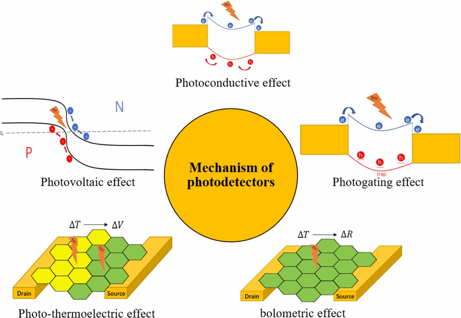
2. Mechanism of photodetectors
In this chapter, the mechanism of photodetection will be introduced. Photodetectors can be divided into two categories: photon-type (photovoltaic effect (PVE), photoconductive effect (PCE), photogating effect (PGE)) and thermal-type (photo-thermoelectric effect (PTE), bolometric effect), as shown in figure 2. Also, the working mechanism is introduced and depicted in figure 3. Meanwhile, all the mechanisms of waveguide-integrated photodetectors reported in recent years are also listed in table 1.
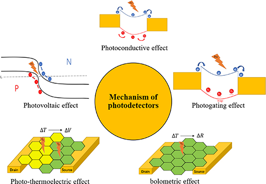
Figure 2. Mechanisms of photodetectors.
Download figure:
Standard image High-resolution image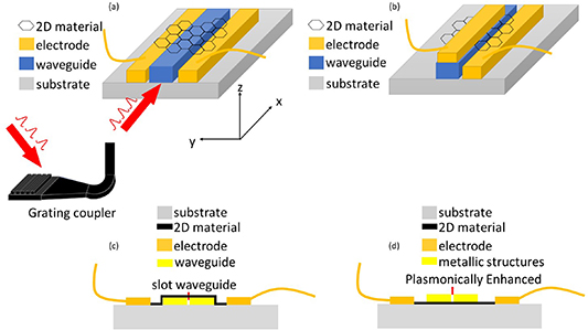
Figure 3. Working process of waveguide-integrated photodetector. (a) Light absorption via evanescent coupling. (b) Vertical structure to narrow the carrier transit path. (c) Slot waveguide to confine light. (d) Plasmonic nanostructure to enhance light absorption.
Download figure:
Standard image High-resolution imageTable 1. Waveguide-integrated photodetectors based on two-dimensional materials in recent years.
| Year | Material | Mechanism | Responsivity | 3 dB bandwidth | Spectral range | Waveguide type | References |
|---|---|---|---|---|---|---|---|
| 2021 | Graphene | Bolometric | 86 mA W−1 | 70 GHz | 1550 nm | Plasmonic slot waveguide | [66] |
| 2021 | Graphene | PTE | 1.4 A W−1 | 100 GHz | ∼1550 nm | Si | [146] |
| 2021 | Graphene | PVE and PTE | 8 mA W−1 | 10–500 Ghz | 6.3–7.1 μm | Si | [38] |
| 2021 | Graphene | PTE | 3.5 A W−1 | 70 GHz | 1550 nm | Si | [9] |
| 2020 | Graphene | Bolometric/PC | 0.4 A W−1 | 40 GHz | 1550 nm | Si | [50] |
| 2020 | Graphene | PTE | 6 V W−1 | 67 GHz | 1550 nm | Si3N4 | [115] |
| 2020 | Graphene | Bolometric/PV | 0.7 A W−1 | — | 1310 nm | Plasmonic slot waveguide | [42] |
| 2020 | Graphene | PV | 360 mA W−1 | 110 GHz | 1540 nm | Plasmonic waveguide | [27] |
| 2020 | Graphene | Bolometric | 25 mA W−1 | 17 GHz | 1550 nm | Si | [139] |
| 2019 | Graphene | PTE | 12.2 V W−1 | 42 GHz | 1.5 μm | Si3N4 | [29] |
| 2018 | Graphene | PTE | 4.7 V W−1 | 18 GHz | 1.5 μm | Silicon photonic crystal defect waveguide | [25] |
| 2018 | Graphene | PC | 15 mA W−1 | 30 GHz | 1550 nm | Si3N4 | [147] |
| 2018 | Graphene | PVE | 13 mA W−1 | 38 GHz | 1550 nm | Si3N4 | [148] |
| 2018 | Graphene | PTE | ∼2.36 A W−1 | 33 GHz | 1550 nm | Si3N4 | [149] |
| 2017 | Graphene | PTE | ≈35 A W−1 | — | 1.55 μm | Hybrid plasmonic waveguide | [150] |
| 2016 | Graphene | Bolometric | 0.11 A W−1 | — | 1550 nm | Si | [48] |
| 2016 | Graphene | PVE/PTE | 0.273 A W−1 | — | 1.55 μm | Silicon slot waveguide | [23] |
| 2020 | Black phosphorus | PCE | 11.31 A W−1 | 0.55 kHz | 3.8 µm | Photonic crystal waveguide | [47] |
| 2019 | Black phosphorus | PVE | 306.7 mA W−1 | 1.33 GHz | 2 µm | Hybrid ridge waveguide | [125] |
| 2018 | Black phosphorus | PGE | 0.48 A W−1 | — | 3.76 μm | Silicon ridge waveguide | [151] |
| 2018 | Black phosphorus | PCE | 40 mA W−1 | — | 2185 nm | Chalcogenide glass waveguide | [109] |
| 2022 | MoTe2/BP | PVE | 0.85 A W−1 | >10 MHz | 2.8–4.1 μm | Si | [152] |
| 2022 | MoTe2 | PVE | 0.4 A W−1 | 34 GHz | 1260–1340 nm | Silicon photonic crystal waveguide | [128] |
| 2020 | MoTe2 | PGE | 0.2 A W−1 | 24 GHz | 1300 nm | Si | [68] |
| 2018 | MoTe2 | PGE | 23 mA W−1 | 1 GHz | 1310 nm | Si | [153] |
| 2017 | MoTe2 | PCE | 4.8 mA W−1 | 200 MHz | 1160 nm | Silicon photonic-crystal waveguide | [24] |
| 2019 | Graphene/MoS2 | PVE | 440 mA W−1 | — | 532 nm | SiNx waveguide | [67] |
| 2019 | MoS2 | — | 2700 A W−1 | — | 1550 nm | SOI rib waveguide | [154] |
| 2022 | PdSe2 | — | 20 mA W−1 | 40 GHz | 1550 nm | Si | [155] |
| 2022 | PdSe2 | PVE | 1758.7 mA W−1 | — | 1260–1565 nm | Si | [129] |
| 2020 | PtSe2 | PCE | ∼12 mA W−1 | 35 GHz | 1550 nm | Silicon nitride waveguide | [130] |
| 2017 | CH3NH3PbI3 | — | 0.012 mA W−1 | — | 1.54 µm | EYS | [135] |
2.1. PVE
The PVE can be explained as a process that photon-excited electron–hole pairs are separated by the built-in electric field oriented by the p–n junction or Schottky barrier. After the electrons and holes get separated, they are forced to transport in opposite directions, generating the photocurrent. Because of the built-in electric field, this type of photodetector needs less exterior bias voltage [12, 28, 29].
The PVE can be found in Schottky photodetectors with the advantages of high responsivity and simple manufacturing process. For example, Goykhman et al reported an on-chip integrated, silicon–graphene plasmonic Schottky Photodetector, showing a responsivity of 85 mA W−1. This waveguide-integrated photodetector utilize the surface plasmon polariton to enhance light–graphene interaction, thus achieving high responsivity. Recently, a new PVE has been summarized, which is called lateral PVE. Lateral photovoltaic effect is caused by the carrier concentration gradient caused by the uneven illumination of various regions of p–n junction or heterojunction. However, their article also mentioned that the relationship between parameters of photodetector and liquid phase exfoliation (LPE) is not clear enough. More experimental research and theoretical analysis are needed to explain the mechanism [30].
2.2. PCE
For the PCE, the incident light is absorbed by 2D material, which generates carriers and increases the material's conductivity. The following formula can express the photocurrent generated by the PCE: IPC = IPH*G, where IPC, IPH, G refer to photocurrent, initial photocurrent and gain (G = τn /τt , where τn means carrier lifetime and τt means carriers' transit time during carriers transport between two electrodes [31]). In some photodetectors, a comb-like electrode is used to reduce the distance between the electrodes, which shortens the transit time and improves the gain. Generally, photodetectors based on PCE need to apply a voltage between two electrodes (source/drain) to promote the separation of electrons and holes. The PCE is usually act as the mechanism of photodetectors based on metal–semiconductor–metal structures [32, 33]. PCE is an important mechanism of photodetectors. For example, Wu reported a waveguide-integrated Bi2O2Se photodetector for Si photonic integrated circuits with low dark current as 72.9 nA, high responsivity as 3.5 A W−1 and fast respond speed with rise/decay time of 22/78 ns [34].
2.3. PGE
The PGE can be regarded as a particular example of the PCE. Because the morphology of the semiconductor is not perfect, there are some defects and nanoparticles in the material. Under illumination, electron–hole pairs are generated in the semiconductor. Subsequently, one of the two carrier types (electrons or holes) is trapped in these defects and acts as a local-area gate tuning the conductance of the channel [35, 36]. One of the pieces of evidence proving that the mechanism of photodetector belongs to PGE is that the threshold voltage of photodetector will change when exposed to light with different optical densities. The photodetector operating in PG mode can obtain a high gain under weak light irradiation. In order to enhance the PGE, quantum dots and some novel materials have been used in photodetectors.
2.4. PTE
PTE is based on the temperature gradient formed by the temperature difference between two positions of semiconductor result from non-uniform light illumination or light absorption of the material. Due to Seebeck effect, a voltage difference is caused by this temperature difference. The Seebeck effect is mainly caused by the diffusion of carriers from the hot end to the cold end. Seebeck coefficient is used to measure the voltage difference caused by temperature difference:

where S refers to the Seebeck coefficient, and where  is voltage change and
  is temperature change [32, 37]. In 2021, Ma et al fabricated a graphene/silicon/halide waveguide-integrated photodetector which achieves long-wave infrared photodetection under zero-bias. They utilized different doping levels in graphene due to metal cover and thus generated Seebeck coefficient in both signal electrodes, which enables effective separation of electron–hole pairs [38].
2.5. Bolometric effect
The bolometric effect refers to the process that local electrical resistivity changes due to light absorption, raising the material's local temperature. From a microscopic point of view, when the energy of photons is insufficient to make the electron transition, the interaction between phonons and low-energy photons will lead to the interference of heat balance and carrier density and change the resistance. The bolometric effect can be found in graphene, Bi2O2Se, yttrium barium copper oxide, etc [39–41]. Ma et al demonstrated a waveguide-integrated photodetector based on graphene operating in two mechanisms, including bolometric effect and PVE with different gate voltage [42].
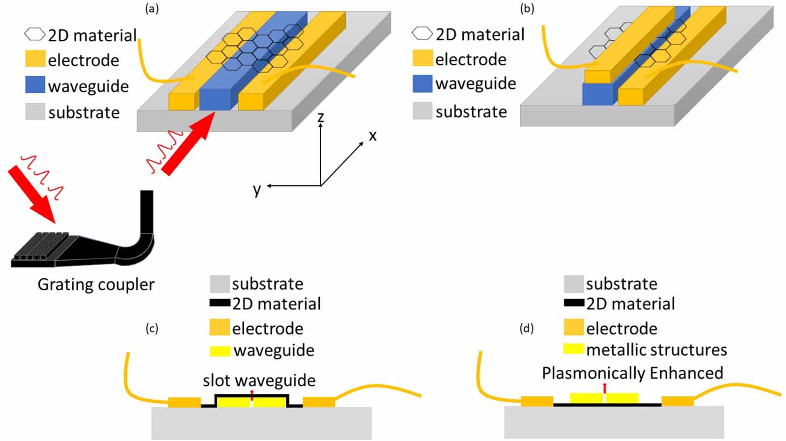
2.6. Working process of waveguide-integrated photodetector
The photodetection process of waveguide-integrated photodetector is as follows: the light enters the optical waveguide through a grating coupler, mode converter or other coupling devices. Here, the function of the coupling device is to couple light and optical mode from optical fiber to the waveguide. The coupling device can improve the coupling efficiency and reduce the loss. Then the light propagates in the optical waveguide and is absorbed by the 2D materials acting as absorption-layer to generate photo-induced carriers collected by electrodes. Finally, the carriers transfer to the circuit and realize photodetection.
There are several types of waveguide-integrated photodetectors. As shown in figure 3(a), light is coupled form optical fiber into the waveguide via grating coupler. Then the light propagates along the waveguide and is finally absorbed by the 2D materials through evanescent coupling. The generated carriers are collected by the external circuit through the electrode. In some designs, in order to shorten the transit time of the carriers, vertical structure is applied in waveguide-integrated photodetectors which narrow the carrier transit path and improve the speed performance, as shown in figure 3(b).
However, with atomic thickness, 2D materials suffered from low and insufficient optical absorption. Researchers have explored several methods to enhance the absorption. Slot waveguide is used to confine the light in the slot due to the discontinuity of the electric field at the high refractive index contrast interface (such as Si and air), as depicted in figure 3(c) [23, 43]. Confined light increases the interaction to 2D material. Another way to strengthen the absorption is plasmonic nanostructure. Plasmonic nanostructure is used to enhanced local electromagnetic fields and create subwavelength confinement induced by metal nanostructures. Plasmonic structures can also be employed as Schottky contacts to increase responsivity [44]. In addition to enhancing the optical response, these structures further reduce the size of the device, making the overall device more compact.
3. Photodetector performance parameter
When measuring the performance of photodetectors, several key parameters will be mentioned. These parameters are briefly described in this chapter.
3.1. Responsivity (R)
Responsivity refers to the ratio of photocurrent to input optical power or the ratio of optical voltage to input optical power. In general, the responsivity will change as the value of wavelength changes. At a certain wavelength, the greater the responsivity, the more carriers each photon can generate.
3.2. External quantum efficiency (EQE)
EQE refers to the ratio of all photogenerated carriers produced by the photodetector to the number of photons incident on the photodetector. The following equation can be employed to illustrate the relationship between EQE and responsivity: EQE =  R, where h is Planck's constant, c is the light speed, e is the amount of charge of a single electron, and λ is the wavelength of incident light.
3.3. Response time and bandwidth (Δf)
Response time is used to measure the response speed of the photodetector. The response time includes rise time and fall time, which are respectively defined as the time interval required to rise (fall) from 10% (90%) to 90% (10%) of the maximum value of photocurrent or photovoltage. The response time is usually related to the carrier mobility of the material, the channel's distance, the applied bias, and the mechanism of photoelectric detection.
The speed of the photodetector mainly depends on its bandwidth. Bandwidth refers to a range between the maximum and minimum working frequencies, which can be expressed by the following equation: Δf = fmax − fmin. Another familiar parameter is 3 dB bandwidth (f3dB), which is defined by the frequency at which the outputresponse drops to 50% (−3 dB) of its maximum value. 3 dB bandwidth can be calculated by the following equation:
where 1/ftr and fRC refers to carriers' transit time and RC frequency. As can be seen from the equation that the 3 dB bandwidth is relevant to carriers' transit time and RC frequency. Carriers' transit time is determined by thickness, width, and other characteristics of the photo-active regions of photodetector. RC frequency is decided by junction capacitance, parasitic capacitance and resistance of photodetector [45].
3.4. Noise equivalent power (NEP)
When the incident optical signal is equal to the noise of the photodetector, that is, when the signal-to-noise ratio is 1, the minimum optical power detected by the photodetector is called the NEP. It can be seen that the smaller the NEP is, the weaker optical power can be detected. NEP is relating with different kinds of noises, including shot noise, thermal noise and 1/f noise. Shot noise is generated from the dispersion of the carriers that form the current and their random emission and collection. Thermal noise is also called Johnson noise, which forms by the electrons' Brownian Motion. 1/f noise is also named as flicker noise, which dominated only under low frequency [2, 46]. In 2D materials, it is found that 1/f noise may be the constraining factor that restrict the performance of 2D-material-based devices. In addition, the reciprocal of NEP as detectivity (D) is defined to measure the ability to detect faint optical signals.
4. Fabrication
In this chapter, several steps of designing and preparing waveguide-integrated photodetectors including analysis of waveguide structure, material preparation and transfer are sketched.
4.1. Analysis and design
For waveguide-integrated photodetectors, the designs of structures of photodetectors and waveguides are critical. As we know, different waveguide structures determine the mode of light that can propagate in the waveguide. In addition, to make the incident light interact with the selected 2D material, the appropriate coupler or evanescent field structure must be reasonably designed so that the incident light energy can be utilized to the greatest extent. Besides, the incident light will encounter various losses in the waveguide, so the structural parameters of the waveguide need to be designed and optimized. Finally, the distribution of electromagnetic fields in waveguide also needs more complex calculations. With the use of simulation software, the above calculation and simulation problems can be solved, and the designs of the waveguides are becoming easier.
4.1.1. Finite-difference time-domain (FDTD) method.
Yee proposed the FDTD method in 1966. It transforms the continuous Maxwell equation in the time domain into a discrete difference equation, simplifying the electromagnetic field's calculation and simulation. The FDTD method has been applied to the analyses of electromagnetic fields and waveguide design. For example, Muench et al utilized the FDTD method to search for the suitable width and position of monolayer graphene with good performance. The transfer of light between the SiN waveguide and the graphene photodetector is simulated by the FDTD method [29]. Wang et al simulated the waveguide optical field distribution by the FDTD method, as can be seen in figure 4(a), which provided helps to improve the design. Ma et al compared the absorption of BP on subwavelength grating waveguides (SWGWGs) and photonic crystal waveguides (PhCWGs) by the FDTD. The results (figure 4(b)) showed that the absorption was weak on SWGWG due to the short length of interaction. However, the optical absorption of BP on PhCWG is enhanced due to the slow light effect [47]. According to the simulation results, they used PhCWGs as integrated waveguide structures on photodetectors.
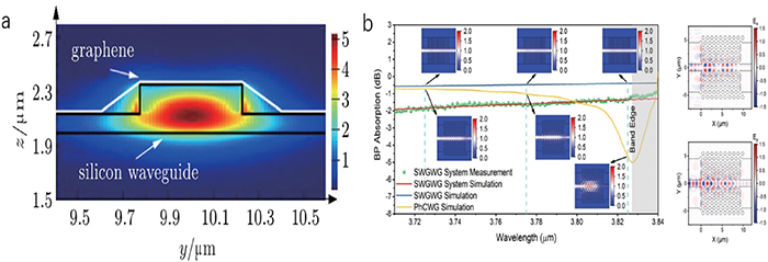
Figure 4. (a) FDTD simulation diagram on graphene–silicon waveguide structure [48]. 2016, © 2016 Chinese Physical Society and IOP Publishing Ltd. (b) FDTD simulation diagram of optical absorption and electric field distribution of BP on different waveguide structures. 2020, Springer Nature.
Download figure:
Standard image High-resolution image4.1.2. Finite element method (FEM).
For the photodetector with waveguide structure, the calculation of light field distribution is critical, which is related to the Maxwell's equation. However, for Maxwell equation, its analytical solution cannot be obtained in many cases, so the FEM can solve this problem well. In addition, the influence of waveguide structure on the optical absorption of materials is also a complex calculation problem, which can also be solved by FEM. The FEM is a process that transforms partial differential equations into linear algebraic equations and then solves boundary value problems. The basic mathematical rule of the FEM is to divide the region into smaller regions (called elements) and then use basis functions (linear function and other low-order functions) to approximate the solution in each element [49]. In the analysis of waveguide integrated photodetectors, FEM is often used to visualize the distribution of electromagnetic fields and modes in waveguides. Guo et al took advantage of the FEM mode solver in COMSOL (a software for modeling and simulation) to analyze the mode of the silicon–graphene hybrid plasmonic waveguide. In addition, they calculated the absorption of graphene and metals to optimize the structure of the waveguide, as shown in figure 5.
Figure 5. FEM simulation diagram. (a) Distribution of electric field. (b) Absorption of graphene [50], 2020, Springer Nature.
Download figure:
Standard image High-resolution image4.2. Preparation for 2D material
In the past decade, lots of methods of preparing materials have been applied to the preparation of 2D materials. From mechanical exfoliation to LPE and pulsed laser deposition (PLD). Different methods have their own merits, advantages, and disadvantages [51]. In this section, these preparation methods and some results in recent years are shown.
4.2.1. Mechanical exfoliation.
Mechanical exfoliation mainly refers to tape or metal-film-assisted exfoliation producing few or even single-layer materials from bulk form materials. The steps of mechanical exfoliation with tapes are as follows: first, put the bulk material on the tape, and then fold and pull apart the adhesive tape repeatedly. With each folding and pulling apart, the number of layers of material will become less and less. Finally, this process can obtain a few layers or a single layer of materials [52]. For instance, Teng et al explored a ground-breaking electrochemical and mechanical hybrid exfoliation (figures 6(a)–(c)), which boosted graphene production [53]. Huang et al invented a technology for automatically exfoliating suspended high-quality graphene. They first prepared SiO2/Si substrate with hole arrays. Then they applied oxygen plasma treatment which helps to exfoliate large area 2D materials (figure 6(d)). Graphene-based field-effect transistor (FET) prepared by this method shows high mobility. This work expands the fields of preparing suspended 2D materials [54]. The superiority of mechanical exfoliation lies in its easy operation. A thin layer of 2D material can be prepared with a roll of tape and bulk material, like the initial preparation of graphene in 2004. However, with the randomness of each exfoliation, it is challenging to realize size-control and large-scale material production.
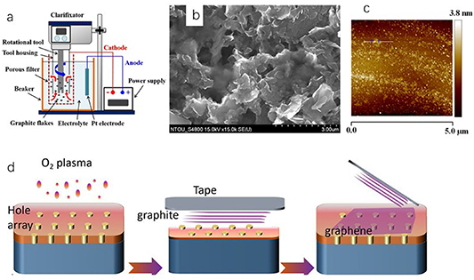
Figure 6. (a) Equipment for electrochemical/mechanical hybrid exfoliation. (b) SEM image of graphene flakes. (c) Atomic force microscope (AFM) image of graphene flakes [53]. 2019,@ Springer-Verlag London Ltd, part of Springer Nature 2019. (d) Suspended high-quality graphene prepared by exfoliation [54]. Copyright © 1999–2023 John Wiley & Sons, Inc. All rights reserved.
Download figure:
Standard image High-resolution image4.2.2. LPE.
LPE refers to separating layered materials by using external forces to overcome the van der Waals force between layers in the liquid phase. The source of external force is mainly from the interaction between the solution and 2D materials [55]. Usually, ultrasonic treatment, ball milling, shearing, and other methods are applied to provide such an external force. Hsieh reported a high-quality BP nanosheet synthesized by LPE (figures 7(a) and (b)) [56]. Ma, DT reported a self-power photodetector employing optimized LPE (figures 7(c)–(e)) to prepare boron nanosheets, showing high responsivity in the ultraviolet spectrum [57]. 2D materials prepared by LPE in recent years are summarized, as shown in table 2. The favorable merit of LPE is that it can synthesize 2D materials with high quality and few layers. However, solvents used for exfoliation are generally toxic (such as N-Methylpyrrolidone (NMP) and N, N-Dimethylformamide). Researchers are looking for environmentally friendly solutions for LPE [58].
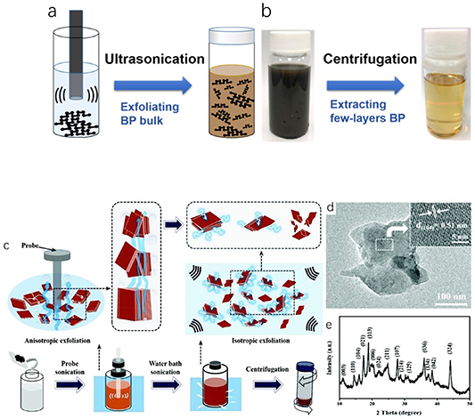
Figure 7. (a) Few layers BP synthesized by LPE (b) SEM images of synthesized BP. 2020, Royal Society of Chemistry. (c) Ultrathin Boron nanosheets prepared by liquid-phase exfoliation. (d) TEM images of Boron nanosheets. (e) XRD pattern of Boron nanosheets [57]. 2020, © The Royal Society of Chemistry 2020.
Download figure:
Standard image High-resolution imageTable 2. Two-dimensional materials prepared by liquid phase exfoliation.
| Year | Material | Solution | Type | Other parameters | References |
|---|---|---|---|---|---|
| 2019 | Graphene | Water/aqueous sodium deoxycholate/ | Ultrasound-assisted | 100 W ultrasonic power/20 kHz in frequency | [156] |
| 2020 | BP | NMP | Sonication | under 30 °C | [157] |
| 2020 | BP | NMP | Ultrasonic/wet ball milling | 400 W Ultrasonic power ball milling in 400 rpm | [158] |
| 2021 | MoS2/WSe2 | NMP | Ultrasonic | 100 W ultrasound power 40 kHz frequency | [159] |
| 2020 | Boron nitride (BN) | Isopropyl alcohol (IPA)/water | Ultrasonic | 20, 30, 40 kHz in frequency | [160] |
| 2021 | Boron nitride (BN) | Ethanol | Sonicate | 50 W ultrasound power 20 kHz frequency | [161] |
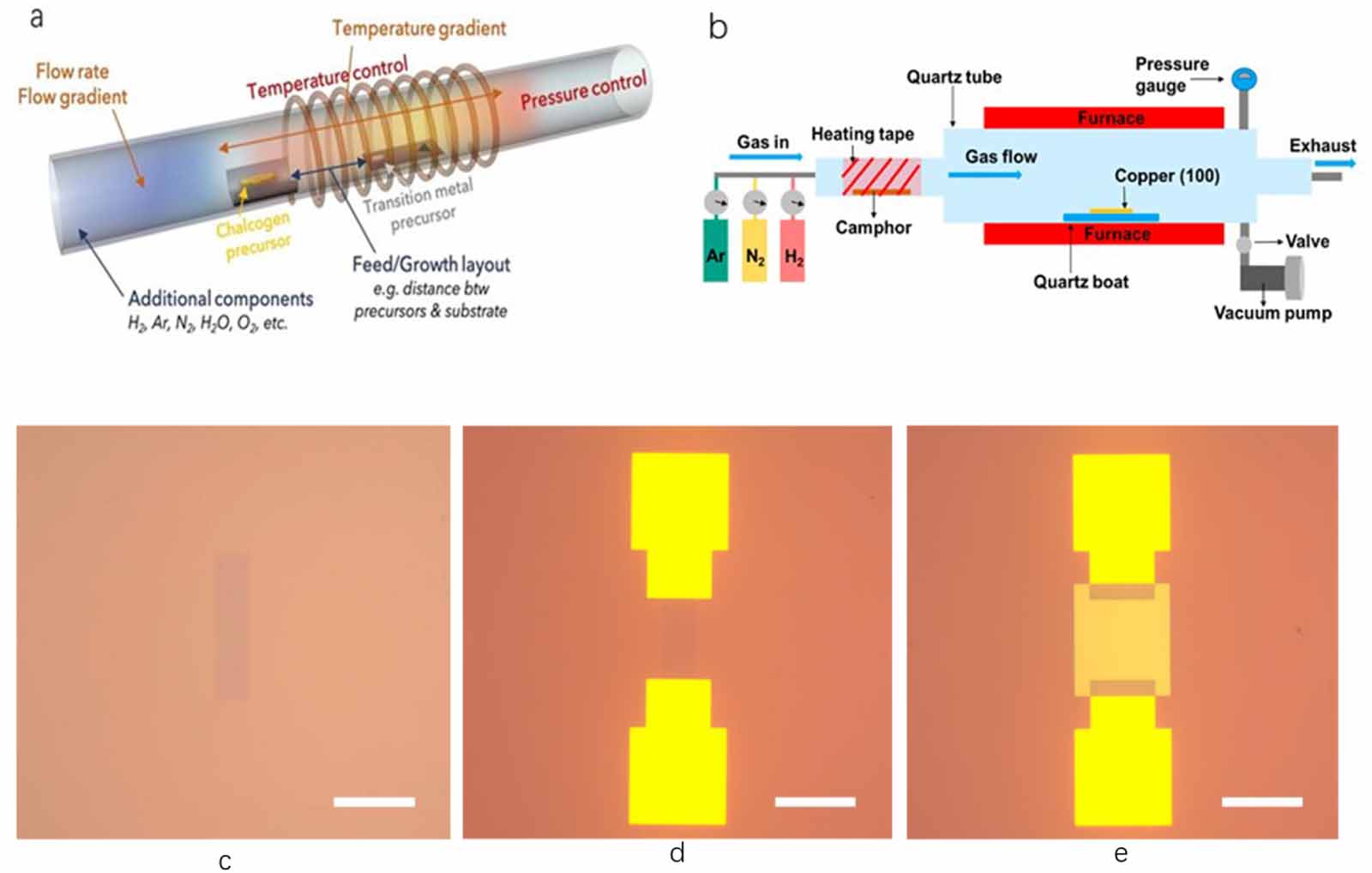
4.2.3. Chemical vapor deposition (CVD).
CVD is a process in which gas or powder precursors are transported by gas to the substrate where materials need to be synthesized. And the chemical reactions occur under an active environment (heating, plasma, light) and finally form solid products such as graphene prepared by CVD technology. (figures 8(a) and (b)) [59, 60]. CVD technology has been widely used in the preparation of various 2D materials, as shown in table 3. For example, Diallo et al synthesized graphene on Ge(100) substrate, revealing the reasons for the formation of pit defects on the substrate, which laid a foundation for the preparation of high-quality graphene [61]. Du et al fabricated a graphene-MoTe2 vertical heterostructure photodetector [63]. Large-area of graphene and MoTe2 are grown by CVD method (figures 8(c)–(e)). The advantages of CVD are as follows: (a) The composition of the whole system is relatively simple. (b) Some CVD system does not need a strict vacuum environment. (c) CVD can synthesize large-area materials. Although CVD technology has been widely used, problems such as high temperature, waste gas treatment, and impurities in the synthesized materials still need to be solved.
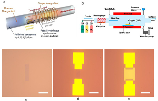
Figure 8. (a) Schematic diagram of a typical CVD equipment [60]. 2020, © 2020 Elsevier Ltd. (b) Device for CVD synthesis. Taking graphene as an example [62]. 2018, © 2018 IEEE. (c) The bottom graphene film grown by CVD. (d) Pd/Au electrodes on graphene. (e) MoTe2 film was transferred and patterned onto the bottom graphene [63]. © 2022 by the authors.
Download figure:
Standard image High-resolution imageTable 3. Two-dimensional materials prepared by CVD.
| Year | 2D Material | Substrates | Gas atmosphere | Temperature (°C) | References |
|---|---|---|---|---|---|
| 2019 | Graphene | Solid phase copper | Ar/H2 | 1060 | [162] |
| 2019 | Graphene | W or Mo | Ar/H2/CH4 | 1090 | [163] |
| 2021 | Graphene | Ge | Ar/H2/CH4 | 910 | [61] |
| 2021 | MoSe2 | Si/SiO2 | Ar/H2 | 900 | [164] |
| 2020 | MoTe2 | Si/SiO2 | Ar/H2 | 650 | [165] |
| 2020 | WSe2 | SiO2/Si | N2/H2 | 780 | [166] |
| 2021 | WSe2 | Sapphire | Ar/H2 | 750 | [167] |
4.2.4. PLD.
The working process of a PLD system is to bombard the target's surface with a focused laser with high energy. Then the target is heated by laser and finally becomes a plasma plume, which is transported to the substrate, condensed, and finally forms a thin film on the substrate. The process is shown schematically in figure 9(a) [64]. Compared with the CVD system, the PLD system usually has a lower operating temperature. Besides, PLD can easily prepare a multilayer structure with fewer impurities [65]. However, impurities still exist because the incomplete ablation of the target will lead to the appearance of impurities when the lasers bombard the target. On the other hand, when the target is bombarded by lasers, the surface morphology of the target will change, which influences the direction of the plasma flow generated by the target and lead to the change in deposition rate. In table 4 below, some examples of 2D materials synthesized by PLD in recent years are shown.

Figure 9. (a) Schematic diagram of a typical PLD equipment [64]. 2019, Copyright © 2021 Elsevier B.V. or its licensors or contributors.
Download figure:
Standard image High-resolution imageTable 4. Examples of two-dimensional materials synthesized by PLD.
| Year | Material | Pressure | Temperature (°C) | Substrate | Laser | Laser energy | Laser wavelength (nm) | References |
|---|---|---|---|---|---|---|---|---|
| 2021 | Graphene | 10−7 | — | Ni/SiO2 | Excimer KrF laser | 5 J cm−2 | 248 | [168] |
| 2021 | Boron doped graphene | 10−7mbar | Room temperature | SiO2 /Si | Excimer KrF laser | 6.2 J cm−2 | 248 | [169] |
| 2021 | WSe2 | 50 mTorr | 600 | MoSe2graphene | KrF-laser | ∼0.8 J cm−2 | 248 | [170] |
| 2021 | SnSe2 | <10−5 Pa | 150 | SiO2 | KrF excimer laser | 150 mJ | 248 | [171] |
| 2021 | h-BN | 10 mTorr | 600 | Stainless steel | ArF laser | 800 mJ/pulse | 266 | [172] |
4.3. Further processing for 2D material and waveguide
After the preparation of the material, the next problem we need to consider is how to transfer the material to the required waveguide structure and pattern the transferred material. In this chapter, a presentation on the technology of transfer and pattern is given.
4.3.1. Material transfer.
After the preparation of the material, the transfer of the material to the waveguide and the material pattern achieved by electron-beam lithography (EBL) and reactive ion etching (RIE) are needed for device fabrication. A common transfer method is wet transfer based on poly(methyl methacrylate) (PMMA). The process is as follows: firstly, a layer of PMMA is spun on the material surface. Then put the combination of substrate, target, and PMMA into deionized water to separate the PMMA attached to the material from the substrate. After that, align the PMMA with the material with the waveguide structure on the transfer station, and remove the residue of PMMA with acetone [38, 66, 67]. In addition to the transfer methods mentioned above, there are many ways for transfer. Bie et al transferred MoTe2 with a transfer device, containing an optical microscope to operate the transfer process. They used an atomic force microscope image to confirm whether the material was aligned with the channel of the waveguide [24]. Also, a pick-up technique based on polydimethylsiloxane (PDMS) or other polymer and mask aligner is applied in the transfer procedure [68].
4.3.2. EBL.
EBL is one of the most widely used lithographic processes. The process can be summarized in the following steps. First, the photoresist is spin-coated on the substrate to be patterned. Then, high-energy electrons are hit on the photoresist by EBL equipment, and the electron beam will react with the photoresist to change its chemical structure. Finally, the whole substrate will be immersed in the developer to remove the unwanted parts, and then the required structure can be obtained by etching or depositing materials. Compared with other lithography technologies, the resolution of EBL is higher due to the very small wavelength of electrons. And that's the reason that EBL is often used in waveguides and material patterning for its high resolution and accuracy [47, 69–72].
4.3.3. RIE.
The purpose of RIE is to remove the part of the material which is unnecessary. The principle of this method is that with the electric field, the etching gas in the reaction chamber is bombarded by high-energy electrons accelerated by the electric field and produces plasma. Then the generated plasma reacts with the etched material surface to produce gaseous products to achieve the purpose of etching [73]. In recent years, RIE methods are also improving. Yamada et al developed a multistep-bias etching method in inductively coupled plasma RIE, reducing the materials' etching-induced damage. Chino et al reported a technique to smooth the titanium's surface in RIE by adjusting the ratio and pressure of the etching gas [74]. After etching, annealing may be required to eliminate defects caused by etching. When the above steps are completed, the device structure is basically fabricated.
5. Waveguide photodetectors based on 2D materials
Researchers have recently combined 2D materials with optical waveguide structures to construct different types of waveguide-integrated photodetectors. Most waveguide-integrated photodetectors are used in infrared spectrum detection. Waveguide integration on the photodetector is of great significance for the miniaturization of the photoelectric system. It has been reported that the light source and photodetectors are integrated on the same silicon substrate [24]. The integrated waveguide-integrated photodetector can be applied in nanophononics, optical communication, and optical interconnection.
5.1. Silicon waveguides
Silicon waveguides have been applied in optical devices such as couplers, sensors, modulators, and optical switches [75–80]. The refractive index of silicon is about 3.4 and the propagation loss of silicon waveguide can be less than 0.5 dB cm−1 [76, 81]. The loss of silicon optical waveguide mainly comes from the light scattering caused by the rough area of the sidewall during processing. In order to reduce the loss of optical silicon waveguides, new structures and methods have also been applied to the preparation and post-processing of optical waveguides. Silicon optical modulator based on silicon multimode interference waveguide with low loss (0.7 dB) is also developed, which utilized fin-type electrode to reduce scattering loss [82]. Tu reported and summarized the recent research progress of optical switches, which can be classified into Mach–Zehnder interferometers and micro-ring resonators. These silicon waveguides based optical switches can achieve switching time in the order of picoseconds, low power consumption of 0.05 mW with a loss of 0.3 dB [75].
5.2. Si3N4 waveguides
Although silicon has made great achievements in photonics, with the continuous expansion of the application range of waveguides, some shortcomings of silicon are gradually emerging, such as low bandgap and two-photon absorption, which leads to limited operating wavelength and nonlinear losses [83–85]. In recent years, silicon nitride has attracted the attention of researchers as another material suitable for photonics that avoids the mentioned shortcomings. With ultra-low optical loss below 1 dBm−1 and strong Kerr nonlinearity, Si3N4 waveguides are ideal platforms for nonlinear photonics with a refractive index about of 1.98. Si3N4 waveguides have been applied in vast optoelectronic devices such as modulators [86, 87], photodetectors [88, 89], sensors [90] and particle detectors [91], Si3N4 waveguides can be fabricated by deep ultra-violet stepper lithography, dry etching, and low-pressure CVD. For the loss of silicon nitride waveguide, researchers found that silicon nitride waveguide has lower sidewall roughness which leads to a reduced loss. With the complexity of the device structure, more and more bends occur in the waveguide, so that the loss caused by bending cannot be ignored. Researchers simulated and optimized the bending loss with three-dimensional FDTD technology. Experiments based on advanced bending shows that the bending loss can be reduced to 0.04 dB/90° [92–98]. With such low loss, silicon nitride is expected to play an important role in next-generation integrated photonic devices.
5.3. Other materials based waveguides
In addition to Si and Si3N4, other materials may also have the possibility be used as waveguide materials in waveguide-integrated photodetectors including LiNbO3, polymer and glass. LiNbO3, as a major role in integrated optical devices, shows several unique properties such as strong electro-optic effect, large refractive index, wide transparency window from UV to mid-IR, and high stability. LiNbO3 has been used in photodetector for its spontaneous ferroelectric polarization that forming a p–n junction photodetector, showing broad detection range and high responsivity as 2.92 × 10⁶ A W−1. Besides, with the wide transparency window, we may use LiNbO3 combined with upconversion or downconversion effects to enable devices under different wavelengths [99–103]. Polymer waveguides have been employed in high-speed optical interconnects systems and photodetectors for polymers' broad transparent window, high flexibility, good processing characteristics of photolithography, and compatibility with optoelectronic device [104]. For photodetectors, detection at a wavelength of 1550 nm has been achieved with SU-8 polymer as the waveguide core material [105]. As for optical interconnects systems, polymer waveguides also give a promising performance as chip-level optical interconnects on a silicon platform [106]. High data transmission rate as 10 Gbit s−1 and low bit error rates better than 10−12 in polymer waveguide-based optical interconnects exhibit the applicability in high-speed data transmission [107]. In terms of glass waveguide, various advantages can be found in glass materials such as low cost of material, being compatible with optical fibers, low propagation loss, birefringence, high stability and reliability [108]. Among these glass waveguides, chalcogenide glass waveguides are used in waveguide-integrated photodetectors. Graphene and BP have been integrated with chalcogenide glass waveguides to fabricate photodetectors, exhibiting high responsivity and NEP low as 30 pW Hz−1/2 at 2185 nm [109]. Chalcogenide glass can be deposited onto 2D materials due to similar van der Waals interactions, which serves as passivation layer and waveguide material. Although some progress has been made in waveguide-integrated photodetectors that utilizing the above materials, there are relatively few reports. By making better use of the advantages of various materials, we look forward to more waveguide-integrated photodetectors made of other materials as waveguides in the future.
5.4. Graphene
Graphene, as one of the 2D materials, is one of the important candidates for developing next-generation optoelectronic devices. Graphene with a honeycomb structure is composed of single-layer sp2 hybridized carbon atoms. The C–C bond between the two carbon atoms makes graphene chemically stable and mechanically flexible [110, 111]. Since it was mechanically exfoliated in 2004, graphene has been wildly applied in optoelectronics for its unique properties, including excellent thermal conductivity, high carrier mobility and other attractive optical, and electrical properties [112]. Lots of optoelectronic devices based on graphene have been reported. However, due to the atomic level thickness, only 2.3% of incident light can be absorbed by graphene, which limits its performance in optoelectronic devices. Researchers have recently integrated the waveguide structures with graphene-based photodetectors, leading to improved light absorption [113, 114].
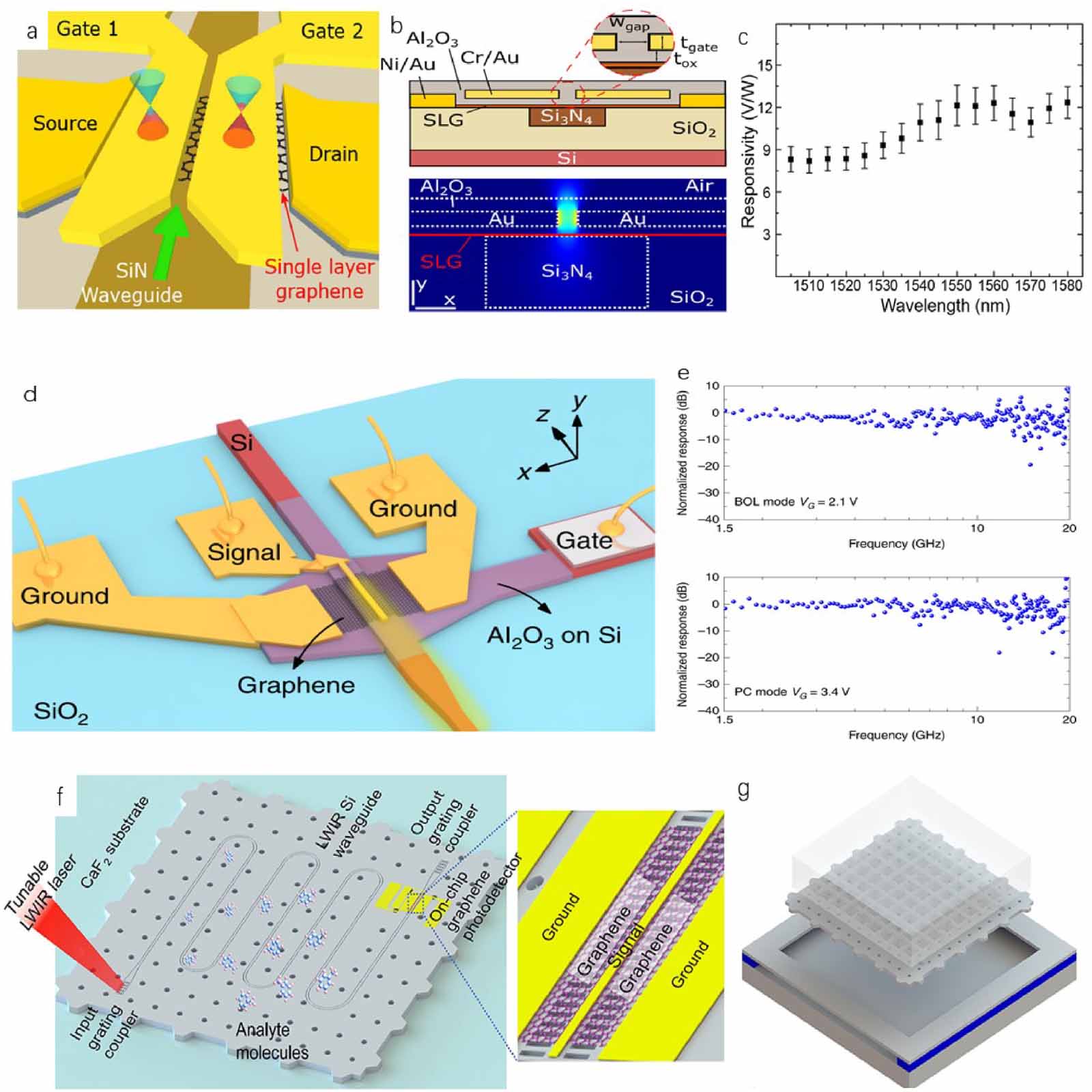
Here, graphene photodetectors with waveguide integration in recent years and their detection performance are shown, as pictured in figure 10. The plasmonic structure has been applied to graphene-based photodetectors to enhance light absorption. In 2018, researchers achieved the combination of graphene and plasmonic structure to prepare a photodetector with a bandwidth above 100 GHz with high responsivity [26]. In 2019, Muench et al reported a waveguide-integrated and plasmonic enhanced photodetector based on graphene with external responsivity ∼12.2 V W−1 and 3 dB bandwidth ∼42 GHz [29]. As can be seen in figures 10(a)–(c), the separated gate will form a p–n junction in the single-layer graphene channel, and the waveguide mode of surface plasmon polariton will be guided. When the incident light propagating to two gates in the silicon nitride waveguide, the optical signal is coupled from the waveguide to the gates. Through such a structure, the optical signal is limited in the gap, which enhances the intensity of optical field and the interaction between graphene and light in the region. In 2020, another plasmonic structure in photodetector was designed by Guo et al [50]. They proposed a waveguide-integrated photodetector based on graphene which introduced an ultrathin silicon–graphene hybrid plasmonic waveguide. In their design, reduced contact resistance of graphene-metal and larger 3 dB bandwidth are achieved by a unique metal-graphene-metal (MGM) sandwich-like structure, as can be seen in figures 10(d) and (e). Besides, the parameters of the silicon ridge and metal strip's dimension in the silicon–graphene hybrid plasmonic waveguide are optimized, leading to a significantly increased light absorption and low metal absorption. According to their results and analyses, the responsivity reached 0.4 A W−1 when operating at 1.55 μm with an over 40 GHz 3 dB bandwidth.
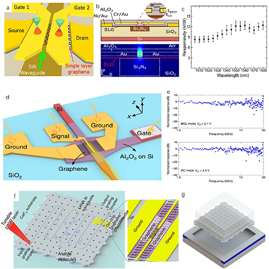
Figure 10. (a) Graphene-based waveguide-integrated photodetector with split-gates as plasmonic slot waveguide. (b) Cross section of the photodetector and simulation diagram of electric field. (c) Wavelength dependence [29]. 2019, Copyright © 2019 American Chemical Society. (d) Device diagram of silicon–graphene hybrid plasmonic waveguide-integrated photodetector. (e) Frequency responses of device [50]. 2020, Springer Nature. (f) Graphene photodetectors based on Si-on-CaF2 folded waveguide. (g) Membrane retrieval by PDMS stamp [38]. 2021,Copyright © 2021 American Chemical Society.
Download figure:
Standard image High-resolution imageIn addition to silicon-based waveguides, waveguides based on other materials are also used in waveguide-integrated photodetectors. Recently, Ma et al reported a Si-on-CaF2 folded waveguide integrated graphene photodetector applied in MIR detection, as shown in figures 10(f) and (g) [38]. They developed a method to fix the problem of the bottom cladding material's absorption, which utilized a microstructured PDMS stamp to transfer waveguides with large-scale membranes, showing low propagation, bending, and insertion loss. It can be expected that there will be more materials applied in waveguide-integrated photodetectors.
Some optimizing methods and designs are applied to graphene-based waveguide-integrated photodetectors. The researchers used the top metal cap as the signal electrode and the MGM structure as the grounding electrode, leading to reduced contact resistance and larger 3 dB bandwidth. In addition, the thickness of the silicon core in the waveguide's vertical direction is changed, making it possible to enhance the optical absorption in graphene due to weak mode field confinement [50]. In another example, researchers also designed a graphene-poly(vinyl alcohol)-graphene structure, which not only keeps the quality of graphene but also enhances the PTE effect [115].
Even though graphene waveguide-integrated photodetectors have made good progress, there is still room for improvement. In the preparation of graphene, although high-quality graphene with high mobility has been prepared, there are still limitations on preparing graphene in a large area. Different defects are often introduced in the preparation process, including the non-uniformity of graphene, the damage caused by the patterning process, which will decrease the quality of graphene [116]. Especially for waveguide-integrated photodetector based on the PTE, the quality of graphene will affect graphene's Seebeck coefficient, thus affecting the generation of photovoltage, responsivity, and noise of photodetectors [9, 29, 38, 50, 66, 68, 115, 117]. Therefore, we also need to optimize graphene's preparation process to improve graphene materials' performance.
5.5. BP
BP is another potential 2D material for photodetection that consists of only phosphorus atoms. Each layer of bulk form BP is connected by van der Waals force. In a monolayer of BP, each phosphorus atom is connected with three adjacent phosphorus atoms with a covalent bond. There are two types of P–P bonds in BP, leading to the anisotropy of BP, which has been confirmed and utilized in experiments. BP atoms in the same layer are not located on the same plane, which forms a fold honeycomb structure. BP shows a layer-dependent bandgap that varies from 0.3 eV (bulk form) to 1.5 eV (layer form), which differs from graphene's zero bandgap. The tunable bandgap makes it possible for researchers to develop photodetectors suitable for different wavelengths [8, 118, 119]. In addition, BP also shows excellent electrical, optical, and mechanical properties and nonlinear characteristics, making it a promising material in various optoelectronic devices [51, 120–123].
Similar to graphene, layered BP still encounters the problem of insufficient light absorption when applied in photodetectors. Therefore, researchers utilize waveguide structures to enhance the light absorption of BP. Here, waveguide-integrated photodetectors based on BP and the relevant parameters are listed in table 1 above.
In recent years, most of the BP photodetectors prepared by researchers have been used in the near MIR spectral range. In 2018, Li et al reported a MIR photodetector based on BP integrated with waveguide achieving a responsivity of 23 A W−1 at 3.68 µm (figures 11(a)–(c)) [124]. The structure of the whole device contains the following parts: an input grating coupler, a single-mode waveguide, a grating output coupler, and a photodetector based on BP above the output coupler. The reason for stronger interaction between light and BP is that when light transmits to the output grating coupler, the optical signal is guided out of the plane and absorbed by BP. When light is transmitted in this subwavelength optical fiber coupler, it will penetrate BP for many times, leading to an enhanced interaction.
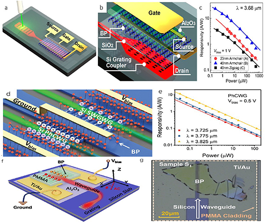
Figure 11. (a) Schematics of the waveguide-integrated with BP photodetector. (b) Larger image of the device. (c) Power-dependent responsivity [124]. 2018, Copyright © 2018 American Chemical Society. (d) Zoom-in image of BP photonic system photodetector. (e) Power-dependent responsivity under different wavelength [47]. 2020, Copyright © 1999–2021 John Wiley & Sons, Inc. (f) Schematic diagram of the hybrid silicon/BP waveguide-integrated photodetector. (g) Microscopy images of the photodetector with PMMA cladding [125]. 2019, ©2019 WILEY-VCH Verlag GmbH & Co. KGaA, Weinheim.
Download figure:
Standard image High-resolution imageBesides, researchers found another way to enhance the interaction between light and BP, which is called the slow-light effect. The slow-light effect means using electromagnetically induced transparency or structures (such as photonic crystals) to reduce the group velocity of light and compress the light energy, the light absorption of materials will be enhanced. Ma et al demonstrated a waveguide-integrated BP photodetector based on the slow-light effect in PhCWGs which reaches 11.31 A W−1 in responsivity and low 0.012 nW Hz−1/2 in terms of NEP (figures 11(d) and (e)) [47].
In addition to weak light absorption, oxidizability is another problem in applying BP in photodetection. Although BP has good photoelectric properties, it is easy to oxidize when it contacts with air or water. This instability seriously restricts the application of BP. In 2019, Yin et al proposed a waveguide-integrated BP-based photodetector, which uses PMMA upper-cladding to avoid oxidation [125]. After 6 months, the device still performed at high speed and high responsivity (figures 11(f) and (g)).
5.6. TMDCs
2D TMDCs, such as MoTe2, PdSe2, and PtSe2 is a class of material whose chemical formula can be regarded as MX2, where M represents transition metals and X means chalcogen. Take MoTe2 as an example. MoTe2 contains 3 phases including 2H, 1T' and Td phase, which show different lattice and band structures. In 2H phase, bandgap varies from indirect bandgap as 0.8 eV (bulk and few-layer states) to direct bandgap as 1.1 eV (monolayer). In 1T' Phase, bandgap reduce to a value of 60 meV. Some TMDCs show similar properties as MoTe2 including layer-decided bandgap (PdSe2 [126], PtSe2 [127]). These adjustable band gaps enable TMDCs to be used in photodetectors with broadband response.
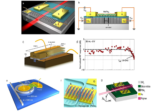
In recent years, researchers have prepared photodetectors with superior performance by combining waveguide structures with TMDCs. Li et al reported a MoTe2 p–i–n homojunction photodetector integrated with silicon PhCWG with high on/off current ratio and response bandwidth under 1260–1340 nm photodetection (figures 12(a) and (b)) [128]. In addition to the infrared spectral region, TMDCs are also used in waveguide-integrated photodetectors for visible light detection. Flöry et al reported a MoTe2/graphene heterostructure waveguide-integrated photodetector with a roll-off frequency of 24 GHz which utilized vertical heterostructure to shorten the transit path of the carriers (figures 12(c) and (d)). Besides, graphene acting as bottom electrodes and built-in electric field generated by the asymmetric contact accelerate the transition of the carriers, which leads to fast response [68]. MoTe2 also integrated with microring resonator (MRR) to developed a strain-engineered photodetector with responsivity as 0.5 A W−1 under 1550 nm and low NEP as 90 pW Hz−1/2. 2D MoTe2 film is wrapped around a non-planarized waveguide to cause localized tensile strain which enhance light–matter interaction, as shown in figure 12(e).
Figure 12. (a) Diagram of MoTe2 p–i–n homojunction photodetector integrated with silicon photonic crystal waveguide. (b) Cross section diagram of the photodetector. Copyright ©2023 American Chemical Society [128]. (c) Diagram of the MoTe2/graphene heterostructure waveguide-integrated photodetector. (d) Normalized radio-frequency (RF) signal response with the thickness of MoTe2 as 35 nm [68]. © 2022 Springer Nature Limited. (e) MRR-integrated MoTe2 photodetector [131]. © 2022 Springer Nature Limited. (f) 3D image of the waveguide-integrated PdSe2 Photodetector [129]. Copyright © 2022 American Chemical Society. (g) PtSe2 polymer waveguide-integrated photodetector [130]. Copyright © 2022 American Chemical Society.
Download figure:
Standard image High-resolution image
In addition to MoTe2, other TMDCs shows attracting potential in waveguide-integrated photodetectors. PdSe2 with adjustable bandgap within the range of 0.03 eV (bulk) to ∼1.3 eV (monolayer) make it a promising candidate for broadband photodetector. A data rate being more than 2.5 Gbit s−1 and low NEP as 4.0 pW Hz−1/2 are achieved in waveguide-integrated PdSe2 photodetector under 1550 nm, as shown in figure 12(f) [129]. High mobility and tunable bandgap of PtSe2 provides suitability for its applications in optoelectronics. High-speed and low dark current are realized in PtSe2-based polymer waveguide-integrated photodetector. Light in the waveguide is guided by structure according to bound states in the continuum [130], as shown in figure 12(g).
5.7. 2D-perovskites
Compared with bulk perovskite materials, 2D layered perovskites show great potential for photoelectric properties. For example, perovskite has high carrier mobility and high photoelectric conversion efficiency. Also, its bandgap can be tuned similar to BP by changing the halide composition. The composition of perovskite can be expressed by the following formula as ABX3. In this formula, A, B, and X represent organic or inorganic cationic material, divalent metal cation and halogen anion respectively. Unlike the traditional preparation method of 2D materials, perovskites are synthesized by space-limit, surface-tension, and spin-coating methods. Perovskite nanosheets with nano thickness have been applied in photodetectors [132–134].
At present, there are few examples of combining waveguide structure with the perovskite-based photodetector. However, part of perovskite waveguide-integrated photodetectors has made some progress. For instance, Zhang et al reported a perovskite–erbium ytterbium silicate (EYS) nanosheet hybrid waveguide-integrated photodetectors with 0.11 mA W−1 in responsivity and 900 μs in response time, which is faster than other reported hot electron silicon-based photodetectors. The upconverted emission property of the EYS nanosheet is availed in photodetectors, which convert light of long wavelength into shorter wavelength. In the experiment, they irradiated 1530 nm light on the photodetector and confirmed that EYS nanosheets would convert the incident 1530 nm light into visible light, which was finally absorbed by perovskite materials [135]. Besides, perovskite photodetectors based optical sensors are demonstrated by Sun et al resolving nanoscale objects as small as 70–80 nm [136].
5.8. Advantages of 2D materials for waveguide-integrated photodetectors
Si/Ge-based photodetectors are the mainstream of photodetectors due to their highly mature manufacturing processes. However, the following drawbacks limit the development of Si/Ge-based photodetectors: (a) dislocations and defects are inevitable during the epitaxial growth at the Si–Ge interface, leading to higher noise in photodetectors. (b) Germanium's poor electrical quality makes it difficult to extend the operating wavelength. Compare with Si/Ge-based photodetectors, waveguide-integrated photodetectors based on 2D materials have the advantages listed below: (a) due to van der Waals forces interaction, there is no dangling bond on the surface of 2D materials, and the lattice matching is not required in the process of epitaxial growth preparation. Compatibility between 2D materials and different waveguide materials is good for the reduction in the size of photonic components on the same chip [43]. (b) 2D materials with high carrier mobility, wide response range across the electromagnetic spectrum and tunable optoelectronic parameters make it suitable to be applied in photodetectors [34, 38].
6. Coupling with other structures and devices
Optoelectronic devices based on 2D materials, such as photodetectors and couplers, have been commonly used in various on-chip platforms and optoelectronic systems using the unique properties of 2D materials. The miniaturization of optoelectronic devices is conducive to further integration of the whole device, making waveguide-integrated photodetectors play a more significant role in optical communication and interconnection. In this chapter, some examples of waveguide-integrated photodetectors based on 2D materials coupling with other structures and devices are illustrated, which further improve the performance of photodetectors, making the photodetectors and other optoelectronic devices act as miniaturized systems.
6.1. Enhancing the performance by combining with other devices
Although waveguide-integrated photodetectors have made some progress, many aspects of performance still need to be further optimized. Such as ohmic loss [137], transmission losses [66], low signal-to-noise ratio and responsivity [43, 50], narrow bandwidth [138]. Due to the above unfavorable problems, waveguide-integrated photodetectors are limited in practical applications. In recent years, researchers have combined waveguide-integrated photodetectors with optoelectronic devices to improve the performance of some aspects of the device, which provides a reference for the direction of further optimization.
In 2020, Li et al designed a waveguide-integrated photodetector with a loop mirror, which showed the compact size and high-speed performance [139]. They achieved great improvement in size and absorption of the graphene-based waveguide-integrated photodetector from two aspects, namely, ultra-thin silicon waveguides and a loop mirror. Compared with conventional 220 nm silicon waveguides, ultra-thin silicon waveguides will reduce propagation loss and enhance the absorption of graphene significantly. However, their disadvantages are the increase in cost and complexity. For the loop mirror, it is designed to reflect residual light back and maximize the incident optical power in the absorption area. Through calculation and simulation, they designed the appropriate bending radius and angle of the ring mirror to ensure the lowest loss. According to their experimental results, the above design shows that more than 80% of the light power is absorbed by the 20 μm active region. Even if the absorption region is shortened, the absorption of optical power is much higher than graphene waveguide-integrated photodetectors previously reported. In addition to the loop mirror, researchers proposed another structure coupled with waveguide-integrated photodetector to achieve high optical absorption. In 2021, Schuler et al integrated a graphene-based photodetector with a MRR [140]. There are two benefits to coupling MRRs. First, the MRR can enhance light-material interaction 10 times before. Secondly, the resonator with wavelength selectivity makes it suitable for wavelength division multiplexing. Based on their experimental results, they realized over 90% of light absorption in a short active region of 6 μm, leading to a high responsivity of 90 V W−1. Besides, zero bias and dark currents are demonstrated in their waveguide-integrated photodetector as the PTE serves as the working mechanism.
6.2. Integrated optoelectronic system by coupling with other devices
Waveguide-integrated photodetectors have considerable freedom in the design of optoelectronic systems. They can work as independent devices or combined with other optoelectronic devices (LEDs or couplers). The compatibility between waveguide-integrated photodetectors and other optoelectronic devices provides an attractive platform for the development of future integrated optoelectronic systems. In this section, several instances of waveguide-integrated photodetector integrating with other devices are introduced.
In 2017, Bie et al demonstrated an integrated optoelectronic system with a transistor, light source, and waveguide-integrated photodetector based on MoTe2 [24]. A response bandwidth of 200 MHz and responsivity of 4.8 mA W−1 are observed. When the integration works in different modes, the interferences between them are relatively small. This investigation gave us a new example of the integration of an optoelectronic system. Huang et al gave us another instance of integration in their research. They constructed a compact combination of BP photodetectors and modulators on the same chip, which achieved a responsivity as 0.3 A W−1 with the working wavelength of 4 μm [141]. However, the protection of BP and the electrical interference between devices still need to be solved. With good adaptability to optoelectronic devices, waveguide-integrated photodetectors also play an important role in optical communication. Wang et al proposed a high-speed optical coherent receiver, which widened the way for optical communication. The optical coherent receiver comprises a multimode interference coupler and four graphene-based plasmonic waveguide-integrated photodetectors. The receiver owes the ability to detect high-speed modulation signals (240 Gbit s−1) in an ultra-low additional power consumption (14 fJ bit−1).
7. Summary, challenges, and prospect
In this paper, the design and advantages of waveguide-integrated photodetector are summarized. The characteristics of silicon waveguides and silicon nitride waveguides are discussed. Then the development of 2D material photodetectors integrated with waveguides in recent years is summed up, mainly focusing on the infrared spectrum region. At last, some examples of the integration between waveguide-integrated photodetectors and other structures and devices are illustrated.
As stated above, waveguide-integrated photodetectors have obtained some substantial achievements. However, challenges still exist in achieving high performance waveguide-integrated photodetectors. Some areas need to be improved as follows:
- (a)For the preparation process, there is room for improvement in the material selection, transfer process, and fabrication of the materials. When the 2D materials are transferred to the waveguide structure, the damage will be produced on the material, which will cause deterioration to the performance of the device [67]. At present, most of 2D materials in the waveguide-integrated photodetectors are prepared by mechanical exfoliation or CVD, followed by transfer process. However, mechanical exfoliation or CVD is not efficient. It is difficult to achieve large-scale production and industrialization. More importantly, impurities or organic residues can be introduced to affect the surface of the material and thus degrade the device's performance. Some 2D materials are easily affected by oxidation and moisture, which generate other impurities. Films or polymers can be deposited to protect the materials from influence [66]. Unique junction structures can be used to reduce the dark current and broaden the spectral detection range of the photodetector [50]. The preparation process of the waveguide needs to be more mature to reduce the loss (bend loss and propagation loss). The crystal orientation of 2D materials and the design of waveguide geometry need to be considered in the preparation of 2D waveguide-integrated photodetectors, which can improve the performance of photodetectors [109, 124, 137].
- (b)There is a trade-off between the performance parameters of the waveguide-integrated photodetectors. The bottleneck difficulty encountered is: waveguide-integrated photodetectors can not simultaneously achieve the properties of high responsivity (100 A W−1), broad bandwidth (3 dB bandwidth ⩾100 GHz) and high-speed data transmission rate (⩾100 Gbit s−1). Although graphene is expected to build high-speed photodetectors due to its high mobility, it is difficult to gain high responsivity due to low light absorption. Moreover, due to zero band gap, photodetectors based on graphene have high dark current, which leads to high shot noise. Compared with graphene, the appropriate band gap of BP can reduce dark current. With the high optical absorption coefficient, BP is expected to achieve high responsivity [25, 68].
- (c)In addition, with the increasing integration of optoelectronic systems and the demand for high-speed and high-capacity optical networks, waveguide photodetectors may work in the form of arrays in the future. The heating problem may become serious, so we also must consider the heat dissipation of large-scale photodetector arrays [142–144].
In the future, it is believed that waveguide-integrated photodetectors will have further development expected as follow:
- (a)Different waveguides can also be integrated with photodetectors, so that silicon waveguides and silicon nitride waveguides are no longer the only choices. As stated above, LiNbO3, polymer and glass waveguide can be used as waveguide materials. The unique properties of these materials can better improve the performance of waveguide-integrated photodetectors. Recently, some researchers have proposed and summarized the latest progress in the research of meta-waveguides [145], which is a set of subwavelength structures with metamaterials and metasurfaces. Using meta-waveguides can diversify the structure of guiding light and achieve more chip-level optical signal processing.
- (b)More 2D materials can be applied to waveguide-integrated photodetectors to further improve the detection range and 3 dB bandwidth of waveguide-integrated photodetectors, which is expected to reach more than 150 GHz. Besides, different 2D materials can construct heterostructures which achieve complementary advantages of both materials and avoid the original performance shortfalls.
- (c)Ni/Au, Ti/Au, Ni/Al and Au are materials that mostly used in waveguide-integrated photodetectors. Compared with the above metal electrode, graphene electrode has superior optical and mechanical properties, lower resistance and lower requirements for complex high vacuum deposition process. Moreover, with the advantages of high transparency, low reflectivity, high current transmission capacity and adjustable Schottky barrier, graphene is also suitable for transparent electrodes, which is suitable in wearable device.
- (d)With the advent of the era of artificial intelligence, machine learning, and other technologies, designs of optoelectronic devices can be optimized, such as the structural design of waveguide-integrated photodetector and intelligent selecting the bandgap of materials. Through the above advanced simulation and computing technology. Waveguide-integrated photodetectors can also be combined with other sensors, such as temperature, pressure, and gas sensors to form a sensing system. Finally, more design of device structures, material mechanism interpretation, and preparation process optimization need to be realized through the efforts in future work.
Acknowledgments
This work was supported by National Natural Science Foundation of China (No. U21A20511), Guangdong Natural Science Foundation of China (No. 2019A1515010007), King Khalid University through Research Center for Advanced Materials Science (RCAMS) under Grant No: RCAMS/KKU/006/21, Science and Technology Innovation Commission of Shenzhen (No. JCYJ20190808175605495), National Natural Science Foundation of China (11674232).
Data availability statement
All data that support the findings of this study are included within the article (and any supplementary files).