
Abstract
We propose an optical setup based on a spatial light modulator (SLM) to facilitate rapid micro structuring such as laser lithography. The beam shaping of the system was addressed and we were able to minimize the effect of common issues of SLMs by adjusting our optical setup. We separated the zero-order focal plane from the first image plane via a focus shift to improve the image quality. This causes a Fourier filtering which is theoretically analyzed. This work explains challenges in filtering the zero-order beam and validates the achievable resolution of ∼11 μm of the proposed setup. The speed of maskless structuring can be improved by this approach while maintaining the resolution. We demonstrated the use of the setup for SLM-based maskless laser lithography.
Export citation and abstract BibTeX RIS

Original content from this work may be used under the terms of the Creative Commons Attribution 4.0 license. Any further distribution of this work must maintain attribution to the author(s) and the title of the work, journal citation and DOI.
1. Introduction
Micro- and nano-structuring is a growing sector in industry, enabling new products in optics and biology. To achieve high design freedom, maskless lithography is preferable, but it lacks throughput. To increase the fabrication speed, multiple beam processing was proposed in several ways including diffractive beam splitters, diffractive optical elements or micro lenses [1–3]. Also, a combination of interference and grayscale lithography was presented for large area application [4]. To fabricate periodic and non-periodic patterns, a very promising method is the use of spatial light modulators (SLMs) [5, 6]. They provide increased flexibility due to their large number of small pixels, are easily programmable and allow a versatile control of the intensity distribution. Consequently, they have been used for beam shaping applications in optical tweezers [7] or adaptive optics [8]. Furthermore, SLMs were used in structuring setups for the micro drilling of holes with sizes ranging from 25 μm to 700 μm [5, 9]. Besides circular shapes, micro channels with similar sizes were achieved in combination with stage movement [10]. Also, SLMs were used for creating microtubes via creating Bessel beams [6]. Periodic structures like woodpile photonic structures were fabricated in SLM lithography reaching sub-micron resolution [11, 12]. For non-periodic patterns, however, arising artifacts limit the resolution and therefore a versatile application in lithography so far. As the frame rate of SLMs has been low, a usage of SLMs in lithography for speeding up the process was very limited compared to e.g. multiple beam structuring. To achieve arbitrary patterns, now SLMs with repetition rates up to 180 Hz and millions of pixels are available. This means there is a big potential to speed up the fabrication compared to sequential galvo scanning.
In this paper, we demonstrate a setup for SLM-based maskless laser lithography. We facilitated the proposed setup of Hayasaki for direct fs-laser structuring [13]. In contrast to working with several holes, our goal was an arbitrary intensity distribution at the focal plane. We created computer generated holograms (CGHs) with different lens functions for the SLM. The optical path was set up to go through a 4f setup. With filtering the zero-order and focus shifting we increased the resolution of the setup. The possibilities and limitations of the resulting system consisting of three lenses plus SLM are discussed, occurring side effects like double peaks are addressed and related to Fourier filtering. Finally, we conveyed lithography on the setup and determined the achievable resolution. We calculated the decrease in fabrication time by keeping a high patterning flexibility.
2. Methods
2.1. Optical setup
The experimental setup is shown in figure 1. An argon-ion laser (Coherent Sabre 25/7, continuous-wave laser) was used with a wavelength of 457.9 nm. The beam was guided through a polarization turner and a beam expander towards the SLM (SLM Pluto-2 Holoeye, 1920 × 1080 pixels). The polarization turner is needed to illuminate the SLM with the correct linear polarized light and the beam expander ensures that the beam covers the SLM's area without illuminating the frame of the display. The central ∼1000 × 1000 pixels of the SLM are used for the modulation of the incident light's phase. This was done to avoid frame artifacts occurring because of over illuminating the SLM. The SLM was oriented at a 13° incident angle. The CGH shown on the SLM was calculated with the Holoeye pattern generator via an input picture. An additional lens function could be chosen to add a focusing, also referred to as phase value. After the SLM, a 4f optical system (lens L1 and lens L2, focal distances 150 mm and 250 mm respectively) with magnification 1.67 was set up. Between L1 and L2 the Fourier plane (FP) of the 4f-system is located, and a Fourier filter was later installed at this position. The focusing lens L3 (100 mm focal distance) was installed right at the end of the 4f-system and creates the final image in the image plane (IP). The chosen focal lengths of the lenses determine the size of the image. In the IP, either a camera or a substrate could be mounted at a motion stage allowing accurate positioning in the focus of the optical system. We examined the image located at the IP with a camera (DMK 72BUC02, pixel width 2,2 μm).
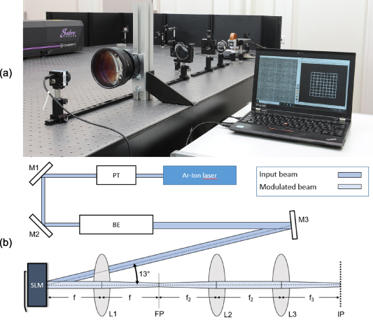
Figure 1. A picture (a) and a sketch (b) of the SLM-based lithography setup with 4f setup, SLM and lens. An argon-ion laser is guided through a polarization turner PT, a beam expander BE and several mirrors M1, M2, M3. The beam hits the SLM at 13° and is modified by the SLM. The 4f setup (lens L1, L2 with focal lengths f and f2) and the lens L3 (focal length f3) are installed and feature the shown Fourier plane (FP) and image plane (IP) of the system. In the image plane the camera or a substrate could be mounted.
Download figure:
Standard image High-resolution image2.2. Filtering the zero-order and focus shift
The beam path of the optical setup is shown in figure 2(a) including the modulation of the laser beam. The SLM allows reprogrammable waveform generation under computer control which transfers to the control of the intensity distribution at the IP [14]. Due to a limited filling factor of the display, an unmodulated sub-beam is also reflected which creates a zero-order spot in the IP, see figure 2(d). The non-normal incident angle on the SLM leads to a different path of the zero-order beam and the modulated sub-beam. When filtering the zero-order in the first IP with a wire, it removes the zero-order spot but also overlays part of the image, see figures 2(b) and (e).
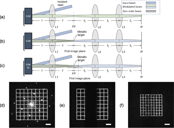
Figure 2. Indicated beam path of the setup (a). The laser beam is phase modulated by the SLM. The intensity distribution at the image plane is shown in (d). The effects of filtering of the zero-order (b) and focus shift FS (c) are sketched and its effect of the image is shown. The resulting images for (a)–(c) are shown are shown in (d)–(f) respectively. The scale bars are 200 μm.
Download figure:
Standard image High-resolution imageThe first IP can be shifted by using a CGH modification. The SLM then acts as a lens in addition to image formation as shown in figures 2(c) and (f). The first image is not formed in the plane of the wire anymore, leading to a full image without showing the wire in the IP. As figure 2(f) shows, the wire does not modulate the image intensity anymore but does a phase modulation which results in a loss of sharpness.
2.3. Image evaluation
By measuring single line widths, it is possible to quantify the resolution capabilities of the setup. In figure 3 vertical and horizontal profiles of the image figure 2(f) are shown. Also shown in the figure 3 is the position of the extracted profiles in the insert on the top right. In figures 3(a) and (b), quality issues are occurring which we will call extended peak (figure 3(a1)), double peak (figure 3(a2)) and non-uniform peak height (figure 3(a3)). The extended peak and the double peak are only occurring in the horizontal axis and are discussed later. The varying peak height can be seen in both profiles. This is due to the speckle interference problem which is a typical drawback of current SLM-based laser marking processes; several methods for reducing this effect like time averaging, shift averaging and Wlodarczyk's picture splitting approach are known [15, 16]. Since this was discussed elsewhere, we want to focus on the line widths achieved. To evaluate them, five-line averages were extracted (figure 3(c) and (d)) and used for evaluation. These show the mentioned quality issues, but they are here less emphasized which makes a reliable evaluation of the line width possible. The five-line averages were evaluated using Gaussian fits adjusted to the actual individual peak width which made an extraction of the FHWM possible.

Figure 3. A horizontal (a) and a vertical (b) profile taken from the camera image figure 2(f). The extracted position is indicated in the insert. The quality issues: extended peak (a1), non-uniform peak height (a2) and double peaks (a3), (b3) occur. A five-line average (c), (d) is used for examination of the line width and here shown with the Gaussian fits and full width at half maximum (FWHM).
Download figure:
Standard image High-resolution image2.4. Lithography
For lithography a sample was installed in the IP of the system. The image pattern which is generated in the focal plane was written into a photoresist. By moving the sample and changing the CGH, the whole area could be structured. In contrast to the conventional point-to-point process, microstructures over a range of few 100 μm are manufactured simultaneously. For sample preparation, the positive resist ma-P 1225G resist from micro resist technology was used. It was spin coated on top of a glass substrate with a rotational speed of 3000 rpm for 30 sec and then baked for 2 min on a hotplate at 105 °C. This resulted in a coating thickness of about 2.5 μm. After the sample was exposed, they were developed with the ma-D 532/S developer solution for 2 min. The lithography samples were characterized with the confocal microscope μsurf from NanoFocus.
3. Results and discussion
The resolution and resulting structure quality was determined for different SLM focal values. Resulting images are shown in figure 4 for the phase values −600, −400, −200 and 0 relating to 23,8; 11,9; 7,9 cm SLM focal length and no focusing of the SLM, respectively. We evaluated the resulting average line widths with standard deviation for different phase values and plotted them in figure 5 for the vertical and horizontal lines.
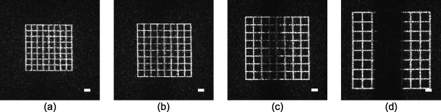
Figure 4. Resulting images using different lens functions on the SLM. The chosen phase values were −600 (a), −400 (b), −200 (c) and 0 (d). The scale bar is 100 μm.
Download figure:
Standard image High-resolution image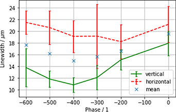
Figure 5. Resulting line widths using different phase values of the SLM. The smallest width could be achieved with phase value −400 for vertical features (solid line), and with −200 for horizontal lines (dashed line). The line between the measured points and the mean value marked with the marker (x) are guides to the eye.
Download figure:
Standard image High-resolution imageWhile decreasing the phase value from zero, the focusing of the SLM increases while the image size decreases and so does the line widths of the grid. From −400 towards −600 an increase in linewidth can be reported. The loss of sharpness is attributed to the discretization error of the SLM. When the virtual focal distance of the lens function is increased, the optimal CGH cannot be displayed due to the limited amount of pixel on the SLM. This effect is decreasing the resolution despite the smaller image size. It can be concluded that phase value −400 worked best for having the highest resolution.
3.1. Fourier filtering of the wire
As stated above, the wire additionally modifies the phase of the modified sub-beam. In order to see the influence on an image when blocking an area in the FP, a picture of a grid was transformed into Fourier space. The grid and its Fourier transform are shown in figures 6(a) and (b), respectively. The wire is working as a blockage of some frequencies, called Fourier filtering. Here, it was assumed to be slightly out of center because of the zero-order beam not going the same optical path as the modified sub-beam. The influence can be illustrated as shown in figure 6(c). The back transformation still produces the image of a grid but with reduced sharpness (figure 6(d)). In figure 6, a vertical (e) and a horizontal (f) profile of the resulting image are shown along with the original profile of the image extracted from the equivalent position.
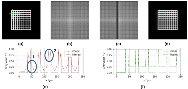
Figure 6. Theoretical analysis of the Fourier filtering with the wire. The Fourier transform (b) of the grid image (a) is modified by the wire (c). A horizontal (e) and a vertical (f) profile of the resulting back transformation (d) are shown. Double peaks (e1) and peak extensions (e2) in vertical profiles as well as a reduced peak-to-valley ratio in horizontal profiles could be observed.
Download figure:
Standard image High-resolution imageWhen comparing the profiles for the vertical lines, the Fourier filtering has the significantly changed the shape of the rectangular pattern. A loss of important frequencies can be identified causing the rectangular pattern not to be reconstructed correctly and show peak extensions (1) and double peaks (2). This relates to the observation from the experiment as shown in figure 4(a). The horizontal lines are not influenced in its sharpness; however, a modified peak-valley ratio can be seen leading to an offset intensity between the lines. It can be concluded that the Fourier filtering as proposed always results in a better vertical resolution (along with the wire) than horizontal resolution (perpendicular to the wire).
3.2. Lithography
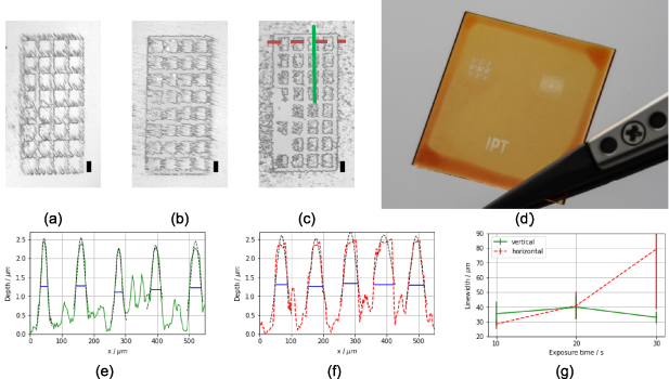
Microstructures such as grids figures 7(a)–(c), micro pyramids and text in various forms (figure 7(d)) fabricated with the setup are shown for exposure times varying from 10 to 30 s. The grid width of the pattern in figure 7(c) was individually evaluated for vertical (e) and horizontal (f) profiles. Figure 7(g) shows the resulting line widths for different exposure times.
Figure 7. Microscope images of the lithography structures showing grids with different widths resulting from the exposure time 10 s (a), 20 s (b) and 30 s (c). The scale bar is 100 μm. The institute lettering as well as micro pyramids was generated to show the structure diversity via a single shot (d). A vertical (e) and horizontal (f) profile from the grid (c) with Gaussian fits and FWHMs is shown. The evaluated widths for each exposure time are compared (g).
Download figure:
Standard image High-resolution image
For 30 s exposure time, the vertical resolution was 33.5 μm ± 1.0 μm and better than the horizontal resolution. Smaller exposure times did not give reliable result, showing too much influence of the speckles to show the expected line widths. It is assumed that the system can be adapted to work also for smaller exposure times leading to line widths as observed in the camera images by implementation of a better focus control when placing the sample.
3.3. Fabrication time
As presented in figure 5, we achieve the minimum resolution for the phase value −400. In this case, the picture size is 1.21 × 1.21 mm2 and the resolution of (10.9 ± 0.6) × (19.3 ± 2.7) μm2; this means an array of 111 × 62 pixels which can be structured at once. The frame rate of the SLM was 10 Hz meaning a structured area of 14.6 mm2 s−1 (68ʹ820 pixels/s). Leading finally to an estimated time of 19.0 h m−2. However, there are already SLMs on the market reaching 180 Hz frame rate, e.g. Thorlabs EXULUS-HD1 with frame boost, meaning a reduction to 25.4 min m−2 (factor 18) seems possible.
4. Summary
In this work, we propose an enhanced approach for controlling an intensity distribution via a SLM. We demonstrated an achievable resolution of (10.9 ± 0.6) μm while introducing a focus shift erasing the zero-order. We discussed the Fourier filtering of the wire which explains the axis dependency of the spatial resolution. It can be concluded that the spatial resolution parallel to the wire is not influenced while the line widths perpendicular to the wire is affected. We examined two sources of sharpness loss, the Fourier filtering of the wire and the discretization error and discussed the dependance on the actual lens function on the SLM. While the influence of the wire on the pattern intensity is small for higher SLM focal values, the discretization error is big and vice versa. With the presented parallel processing approach, the fabrication time has the potential to be 25.4 min m−2. We fabricated microstructures and demonstrated the use of the setup as SLM-based maskless laser lithography.
Data availability statement
The data that support the findings of this study are available upon reasonable request from the authors.