

Abstract
Cesium lead halide (CsPbBr3) perovskite nanomaterials exhibit attractive optical properties, particularly in higher nonlinear optical effects and larger multiphoton absorption efficiency, compared with conventional semiconductors. The unique feature of stable lasing action under photon pumping conditions grants such materials great potential in photonics. Herein, through an in-depth study of the growing mechanism, all-inorganic perovskite nanomaterials with a high crystalline quality and tunable morphologies were synthesized, by a modified physical vapor deposition procedure. The prepared nanowire laser not only presents a high-performance laser output under single-photon pumping conditions, but also maintains decent behavior under two-photon pumping conditions. Importantly, the temperature-dependent fluorescence spectroscopy test of the nanowires reveals that the high exciton binding energy, twice as large as the thermal disturbance at room temperature, is the dominant reason for maintaining stable lasing under high energy density injection conditions.
Export citation and abstract BibTeX RIS
1. Introduction
With the continuous development of integrated circuits, the electronic manufacturing process is getting closer to its physical limits [1], and it is particularly important to develop integrated electronic-photonic chips to further increase speed and lower energy consumption of electronic systems [2, 3]. For the photonic aspects, the miniaturization of coherent light sources is the top priority [4], and seeking ideal gain materials and device structures has always been of importance to realize applicable integrated electronic-photonic chips [5]. In particular, nanowire and nanosheet lasers are regarded as one category of ideal miniaturized lasers [6, 7]. The corresponding flat end faces form a resonant cavity structure, without the construction of external additional resonators [8]. Lots of efforts have been devoted to this promising community for optimizing the device structure and finding ideal gain materials [9]. Recently, cesium-lead halogen perovskite nanomaterials with impressive optical properties (e.g. adjustable band gap in the visible light range [10], up to 100% fluorescence quantum yield [11], and good thermal stability [12] etc) have attracted much attention and have become a hot research focus. Particularly, cesium-lead bromide perovskite (CsPbBr3) combining good stability and high gain performance, is regarded as a good candidate for laser gain material and is broadly applied in single-photon pumped amplified spontaneous emission and lasers [13–22], exciton–polariton lasers [23], and plasmonic lasers [24]. At present, there are mainly two ways of growing perovskite materials, the liquid phase method [25–27] and chemical vapor deposition (CVD) method [28–30]. The liquid phase method has the characteristics of low cost and high product yield, but the uncontrollable crystallinity of the resulting materials makes it difficult to meet the needs of high-performance devices [31]. The perovskite materials grown by CVD show a good crystallinity, but the high energy consumption, harsh reaction conditions and relatively low yield of the growth process are limiting to large-scale application [32]. In the past two years, a physical vapor deposition (PVD) method with advantages of low energy consumption, high yield, and good crystallinity of materials, has been proposed [33]. Such a method is also beneficial for large-scale production [34].
The current mainstream integrated chip technology is still based on silicon material [35], and the suitable optical band of the silicon material system is in the long wavelength range (>800 nm) [36]. This is incompatible with perovskite materials. In order to solve this problem, herein, by modifying the PVD procedure, we prepared high-quality CsPbBr3 nanomaterials with high nonlinear optical effect and large multi-photon absorption efficiency. The CsPbBr3 nanomaterials could be turned to verities of morphologies (e.g. nano dots, hexagonal nanosheets, quadrilateral nanosheets and nanowires), through finely manipulating the growth parameters. The resulting nanowire lasers present a threshold of 12.2 μJ cm−2 and quality factor of Q = 1078 under single-photon pumping conditions. Interestingly, under the two-photon pumping condition, although the threshold has been increased to 26.9 μJ cm−2, and the quality factor remains at a high level of Q = 772. The revealed high exciton binding energy (E = 51 meV) of such a promising material is responsible for the impressive lasing actions.
2. Experimental
2.1. Preparation of CsPbBr3 nanowires
All the chemicals were purchased from Sigma-Aldrich unless otherwise stated. 460 mg PbI2 (99.999%) was dissolved in 1 ml anhydrous dimethylformamide, stirred at 70 °C for 12 h, then the solution was spin-coated on the glass surface at 3000 revolutions per minute for 30 s, and then dried at 100 °C for 15 min. The glass slide covered with lead iodide was immersed in 4 mg ml−1 CsBr (99.999%) @methanol (99.8%) solution and reacted at 60 °C for 12 h. After the reaction, the glass slide was cleaned with isopropanol solution and blow dry with high purity nitrogen. After the drying was completed, the CsPbBr3 precursor was prepared.
Then, the prepared CsPbBr3 precursor was placed on the lower heating plate of the modified PVD device, and the mica substrate was fixed on the upper heating plate. Through setting the temperature of the lower heating plate to 650 K and the temperature of the upper heating plate to 580 K, the reaction was maintained for 5 min. Finally, CsPbBr3 nanowires were obtained on the mica substrate. With different upper heating plate temperatures, CsPbBr3 nanomaterials with different morphologies could also be realized. The schematic diagram of the experiment is shown in figure S1 (available online at stacks.iop.org/JPD/54/275103/mmedia).
2.2. Characterization
The XRD data were acquired on a Rigaku SmartLab diffractometer with 2θ range of 10°–60°. The morphology micrograph measurements were carried out using an optical microscope (BX51, Olympus). The transmission electron microscope (TEM) images were acquired on a JEM-2010 (Japanese electronic optical co, LTD) with an operating voltage of 120 kV. Energy dispersive x-ray spectroscopy (EDS) measurement was also performed from this integrated TEM equipped with an Oxford Inca EDS for the element distribution of the nanowires.
2.3. Optical measurements
The 800 nm femtosecond laser used in the experiment has a pulse duration of 130 fs and a repetition frequency of 1 kHz. The 400 nm femtosecond laser is generated from the second harmonic of the 800 nm laser by the regenerative amplifier (Spectra-Physics Spitfire amplifier seeded by Tsunami oscillator). The pump light is focused on the nanowire to be measured through an objective lens with a magnification of 40 times and NA = 0.65, and the laser spot is guaranteed to completely cover the nanowire. The emission of each nanowire was collected by the same objective lens and focused into a spectrograph (Princeton Instrument, Acton SP2300i) with a 300 mm−1 grating and a liquid-N2-cooled CCD (Princeton Instruments, Pylon camera). Temperature dependent photoluminescence (PL) was measured at 405 nm with 0.5 mm2 spot size. The samples were mounted in a closed-cycle helium refrigerator of CTI Cryogenics. Valid spectra were collected from 30 K to 300 K.
3. Results and discussion
In the conventional growth of perovskite nanomaterials by the PVD method, only the temperature of the perovskite precursor was controlled [34], while the temperature of the substrate was indirectly impacted by the heat radiation and heat conduction of the precursor. In this case, the temperature of the substrate was difficult to control accurately and this hinders the understanding of the detailed mechanism of the PVD method for growing perovskite nanomaterials. In our work, we modified the instrument used in the PVD method, and a dual-zone temperature control device was used to accurately control the temperature of the precursor and the substrate, respectively. The device diagram is shown in figure 1(a), where the glass sheet attached with the perovskite precursor film is placed on the temperature control platform below, with temperature T0; the mica substrate is fixed on the upper temperature control platform, with temperature T. Additionally, the upper temperature control platform is equipped with a circulating water-cooling system to prevent the impact from the thermal radiation of the lower platform. Such a design generates a greater temperature gradient in the chamber and the resulting materials would be of promise in constructing the nanolasers (figure 1(b)).
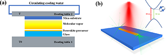
Figure 1. (a) Modified dual-zone temperature-controlled physical vapor deposition equipment. (b) Schematic diagram of two-photon pumped nanowire laser.
Download figure:
Standard image High-resolution imageBy keeping the precursor temperature T0 constant at 620 K, the material growth procedure could be well manipulated by varying the substrate temperature. As shown in figure 2(a), when the temperature of the substrate is selected as 470 K, a large density of uniform nano dots could be well observed. The large temperature gradient between the precursor and the substrate makes the nucleation rate quite fast [37]. The vapor molecules quickly condense and nucleate after encountering the substrate and cannot continue to diffuse and flow on the substrate. The materials with more categories of morphologies could also be achieved. With the gradual increase of the temperature from 470 K to 490 K and 510 K, hexagonal nanosheets can be grown on the substrate. The increased temperature of the substrate decreases the nucleation rate of the vapor molecules. In this case, the molecules would not nucleate immediately but diffuse along the surface of the substrate and eventually grow into a two-dimensional material with a continuous surface [38]. The higher the temperature results in the stronger the fluidity, and the proportion of two-dimensional materials is further increased. When the temperature gradually increases from 530 K to 550 K and 580 K, the hexagonal nanosheets disappear, and the quadrilateral nanosheets and nanowires appear in sequence. Different crystal faces of perovskite materials have different binding energies, and a certain crystal face only grows epitaxially in a suitable temperature range [34].

Figure 2. (a) Optical image of the perovskite material with nano dots morphology. (b) Optical image of the perovskite material with nano dots morphology transforming to hexagonal nanosheets morphology. (c) Optical image of the perovskite material showing the increased proportion of hexagonal nanosheets. (d) Optical image of the perovskite material showing that the hexagonal nanosheets disappears, and the morphology of quadrilateral nanosheets appears. (e) Optical image of the morphology of quadrilateral nanosheets transforming into nanowires. (f) Optical image of the morphology of full nanowires.
Download figure:
Standard image High-resolution imageWe have investigated the perovskite crystal structure and the results are shown in figure 3. The (111) plane has the sixth symmetry, the (100) plane has the fourth symmetry, and the (110) plane has the second symmetry. This corresponds to the symmetry of hexagonal nanosheets, quadrilateral nanosheets and nanowires. The XRD test results show that the different morphologies are just the result of the material growing on the substrate along different crystal planes.
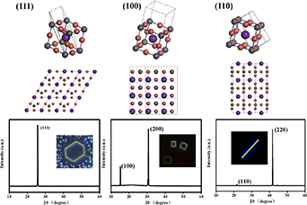
Figure 3. The distribution of atoms on different crystal planes of cubic crystal system perovskite materials and the corresponding XRD patterns of nanomaterials with different morphologies. The XRD test results of hexagonal nanosheets show that the (111) plane is dominant, the results of quadrilateral nanosheets show that the (100) plane is dominant, and the results of nanowires morphology materials show that the (110) plane is dominant.
Download figure:
Standard image High-resolution imageAlternatively, the material growth could also be manipulated by varying the precursor temperatures. As shown in figure S2, the increased precursor temperature from 650 K to 680 K and 700 K makes the surface density of the nanowires gradually increase, due to the enhancing evaporation rate of the precursor. The corresponding increased number of atoms evaporated to the surface of the mica substrate per unit time in turn leads to an increase in the areal density. However, further increasing the evaporation rate deteriorates the morphology of the nanowires gradually, accompanying by the appearance of the uneven thickness and step-like defects. Therefore, we have provided an accurate approach to control the morphologies of all-inorganic perovskite nanomaterials. The specific growth mechanism diagram is shown in figure S3.
Although the nanosheet structure can also support the generation of coherence light, the characteristics of the whispering gallery mode resonance result in more light emission directions than nanowire lasers. Compared with nanosheet lasers, nanowire lasers have a more controllable light direction and are more suitable as coherent light sources. Therefore, this article focuses on studying the properties of perovskite nanowire lasers. Choosing appropriate perovskite nanowires is of significance for the construction of nanolasers. The nanowires provide the Fabry–Pérot cavity resonant mode, and the size is crucial for the lasing action. To make sure that the gain can overcome the loss, the diameter and length cannot be too small. Additionally, nanowires with too large a size would have a relatively large density of internal defects, and this affects the performance of the laser. After considering the mutual influence between gain and loss, nanowires with a length of about 10 μm and a diameter of about 400 nm are finally selected as the candidate gain material for the CsPbBr3 nanowire laser.
Figure 4(a) shows the TEM image of the synthesized nanowire. It can be seen that the surface of the nanowire is smooth, and the end surface is flat, and this can provide a suitable cavity environment for the laser. Figure 4(b) presents the high-resolution transmission electron microscope image of the nanowire and clear crystal lattice could be well observed. The sharp selected area electron diffraction in the inset image also proves that the nanowire consists of s cubic crystals and has good crystallinity. In addition, the element mapping results in figure S4 show that each element is evenly distributed in the nanowire.

Figure 4. (a) TEM image of the as-grown nanowire, length is ∼10 μm, diameter is ∼400 nm. (b) The high-resolution transmission electron microscope (HRTEM) photo of lattice fringe. The inset is the photo of select electron diffraction pattern.
Download figure:
Standard image High-resolution imageFirst, we investigate the performance of nanowire lasers under single-photon pumping conditions. Under the pump of a 400 nm femtosecond laser, the fluorescence spectrum of CsPbBr3 nanowires varies with the pump energy density as shown in figure 5(a). In the scenario of lower pump energy density, the fluorescence intensity and the spectral linewidth are relatively low and wide, respectively. This is the typical characteristic of spontaneous emission. When the pump energy density increases to 12 μJ cm−2, the spectral peak becomes very sharp, reflecting the typical properties of stimulated emission. The FWHM of the curve is reduced to less than 1 nm.

Figure 5. (a) Fluorescence spectra of different energy densities under single-photon pumping conditions. The inset is the photo of nanowire lasing. (b) Curves of output energy and FWHM with input energy.
Download figure:
Standard image High-resolution imageAs shown in figure 5(a), a bright laser light is emitted from both ends of the nanowire, and interference fringes caused by the laser can also be observed around the end points. Figure 5(b) shows the variation curve of output energy and spectral FWHM with input pump energy. The input and output energies present a typical S-shaped curve. Accordingly, it can be judged that as the pump energy density increases, the spontaneous radiation gradually changes to stimulated radiation. At the pump energy density of 12.2 μJ cm−2, the S-shaped curve has an inflection point, and such a point could be considered as the threshold of the nanowire laser. This value is significantly lower than the previous perovskite nanowire laser grown by the PVD method [33], thanks to the well-controlled morphology and high crystal quality. As shown in figure S5(a), the FWHM is narrowed to 0.5 nm, and the quality factor of the laser is obtained as 1080 according to the relationship of Q = λ/Δλ [39] (where λ is the peak center wavelength and Δλ is the peak width), also proving the good lasing behavior of the laser.
To further broaden the application of CsPbBr3 nanowire materials in the laser field, utilizing the high nonlinear optical two-photon absorption effect [40, 41] of the perovskite material is of promise. We have studied the lasing properties of CsPbBr3 nanowire lasers under two-photon pumping by replacing the 400 nm femtosecond laser with an 800 nm femtosecond laser. The curve of the fluorescence spectrum with the pump energy density is shown in figure 6(a). The profile of the curve is basically the same as that in the single-photon pumping mode, except that in the two-photon pumping mode. A higher energy density is required to excite the CsPbBr3 nanowire to emit light. As the pump energy is lower than 10 μJ cm−2, the nanowire device exhibits a typical spontaneous emission. While the pump energy is larger than 30 μJ cm−2, the laser shows the prominent property of stimulated emission. The curve of output energy and spectral FWHM with pump energy density is shown in figure 6(b). The relationship between output energy and pump energy density is standardly S-shaped, suggesting the transition from spontaneous radiation to stimulated radiation. The threshold is only 26.9 μJ cm−2. By Gaussian peak fitting, the FWHM is only 0.8 nm and a high quality factor of 772 is realized, shown in figure S5(b). This result demonstrates that the CsPbBr3 nanowire laser still maintains decent lasing behavior under two-photon pumping conditions.
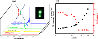
Figure 6. (a) Fluorescence spectra of different energy densities under two-photon pumping conditions. The inset is the photo of nanowire lasing. (b) Curves of output energy and FWHM with input energy.
Download figure:
Standard image High-resolution imageAlthough the threshold of the laser under the two-photon pumping condition is higher than that in the single-photon mode, the magnitude of the change is consistent with the CsPbClx Br3−x nanowires reported [42]. It is worth noting that the threshold under the two-photon pumping condition in our experiment is only one-tenth of that reported [40]. According to previous studies [43], under the condition of high energy density injection, the main mechanism of light emission in perovskite materials gradually shifts from free carrier recombination to the exciton recombination process, and even changes to the electron–hole-plasma luminescence mechanism as the injection energy density increases. Therefore, the physical properties of excitons in perovskite materials are an important part of the study of their luminescence process. In addition, it has also been well reported that the size of the semiconductor material significantly affects the exciton binding energy of the material, thereby affecting the light-emitting performance of the material [44]. Bastard et al calculated in detail the influence of quantum well width on exciton binding energy [45], and Elward et al found through calculations that the exciton binding energy in CdSe quantum dots decreases as the material size increases [46]. By comparison, it can be concluded that the length and diameter of the nanowires used in this experiment are half of those reported in the literature. In addition, the delocalization caused by the small size would increase the two-photon absorption cross section of the material. It has been reported that the two-photon absorption cross section of the two-dimensional perovskite material is an order of magnitude higher than that of the bulk material [47]. Therefore, we believe that the reason for the low threshold under two-photon pumping conditions comes from the increase in exciton binding energy brought by reducing the material size, which in turn improves the performance of the CsPbBr3 nanowire two-photon pumped laser.
To explore the physical reason for the prominent performance of the two-photon pumped perovskite nanowire laser, the CsPbBr3 nanowire was tested with temperature dependent fluorescence spectroscopy. The fluorescence spectra of CsPbBr3 nanowires at different temperatures are present in figure 7(a). With the decrease of temperature from 300 to 33 K, the luminescence intensity of CsPbBr3 nanowires gradually increases, but the luminescence peak position has a red shift phenomenon. This is completely opposite to the blue shift phenomenon of other semiconductors as the temperature decreases. The temperature dependent fluorescence spectra were further analyzed, by double exponential fitting the luminous intensity and temperature with the formula [48]:

Figure 7. (a) Fluorescence spectra of nanowires at different temperatures. As the temperature decreases, the intensity of the fluorescence spectrum gradually increases, and the center wavelength gradually decreases. (b) Fluorescence spectrum intensity and temperature fitting curve.
Download figure:
Standard image High-resolution image
where I0, C and KB represent the PL intensity at 0 K, a fitting constant and the Boltzmann constant, respectively. The double exponential fitting was used to explore the respective effects of free electron recombination luminescence and exciton recombination luminescence in perovskite materials and its corresponding activation energy.
As shown in figure 7(b), the reason for adopting double exponential fitting is that we believe that the luminescence process of perovskite nanowire materials is more complicated. There is not only exciton luminescence, but also recombination caused by defects. Therefore, a double exponential fit is used to calculate the energy required for the two thermally activated quenching processes. The activation energy E1 corresponding to the process 1 (C1 = 4) is 13 ± 1 meV, representing the activation energy caused by defects. The activation energy E2 corresponding to the process 2 (C2 = 161) is 51 ± 6 meV, representing the exciton binding energy of CsPbBr3 [48]. The results of our calculations are consistent with those reported in the literature [48], except that the exciton binding energy is larger. This value is larger than 26 meV at room temperature. Even under high energy density injection, heat accumulation would not cause exciton emission quenching. This provides the right explanation for why the two-photon absorption at high energy density under pumping conditions occurs and the device still presents prominent lasing actions.
4. Conclusions
Herein, we have proposed a method to grow all-inorganic perovskite nanomaterials and control the morphologies precisely, through a PVD process. It is the first time this method has been used to grow nano dots and perovskite nanomaterials with a hexagonal nanosheet morphology, which broadens the application prospect of this method in the field of perovskite optoelectronic devices. By selecting the appropriate nanowire, the two-photon pumped nanowire laser with low threshold and high quality factor was successfully realized. Temperature dependent fluorescence spectroscopy revealed that high exciton binding energy is responsible for the attractive lasing actions.
Acknowledgments
This work was mostly supported by the National Key Research and Development Program of China (Grant No. 2018YFE0204000), the National Natural Science Foundation of China (Contract Nos. U20A20206, 51972300, 62011530022 and 21975245), the Strategic Priority Research Program of the Chinese Academy of Sciences (Grant No. XDB43000000), and the Key Research Program of Frontier Science, Chinese Academy of Sciences (Grant No. QYZDBSSW-SLH006). K L appreciates the support from the Youth Innovation Promotion Association, the Chinese Academy of Sciences (No. 2020114), and the Beijing Nova Program (No. 2020117).
Data availability statement
All data that support the findings of this study are included within the article (and any supplementary files).