

Abstract
Magnetic field sensors using the tunnel magnetoresistance (TMR) effect require linear resistance–magnetic field (R–H) response curves with small hysteresis, for which the soft magnetic property of the free layer (FL) is critical. In this work, we investigated amorphous CoFeBTa (CFBT) as a soft magnetic layer of the FL of CoFeB/MgO/CoFeB-based magnetic tunnel junctions in view of magnetic, TMR, and low-frequency noise properties. A two-step annealing process enabled an orthogonal magnetization configuration between the FL and the reference layer, by which linear R–H curves with small hysteresis were realized. The change in the shape of the R–H curve depending on annealing temperature is explained by the Stoner–Wohlfarth model. The highest TMR ratio of ∼160% and sensitivity of ∼70%/mT were obtained with a CFBT (20 nm)/Ta (0.3 nm)/CoFeB (3 nm) FL. The noise of the TMR devices are dominated by 1/f noise below ∼10 kHz in frequency, which limits the detectivity (D) of the magnetic field of the sensor. The sensor devices patterned to 50 µm diameter circular shapes showed a minimum D of ∼2 nT/ at 10 Hz, which is superior to the previously reported values for the TMR sensors with NiFe soft magnetic layers.
Export citation and abstract BibTeX RIS
1. Introduction
Tunneling magnetoresistance (TMR) devices based on CoFeB/MgO/CoFeB magnetic tunnel junctions (MTJs) [1, 2] are considered to be suitable for various magnetic field sensor applications covering a wide range of magnetic fields from pT to mT, depending on the design of the magnetic properties of the TMR sensor [3]. A convenient figure of merit for magnetic sensors is detectivity (D), which is also expressed as magnetic field resolution or magnetic field equivalent noise level, defined by
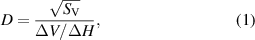
where  is noise voltage density in V/
 , ΔV is the full output voltage and ΔH is the range of magnetic field that the magnetic sensor covers. For magnetoresistive (MR) sensors,
  , where ΔR/R0 is the MR ratio and Vb is the bias voltage applied to the sensor. It is important to obtain low noise and high sensitivity to achieve the sufficiently low D required for the application of the magnetic sensor. For biomagnetic sensors, such as for magnetocardiography and magnetoencephalography, D must be in the order of pT/
 or even smaller in a low-frequency regime, typically below 100 Hz [4].
TMR devices with spin-valve structures usually show a sharp switching of resistance (R) between the low-resistive parallel (P) magnetization state and the high-resistive antiparallel (AP) magnetization state, which corresponds to the magnetization reversal of the free layer (FL) by external magnetic field (H). Hence, the scheme for linearization of the R–H response curve is important for the design of TMR magnetic sensors. A gradual change of R as H changes is realized by introducing a magnetic anisotropy in FL that is orthogonal to the direction of H. For this purpose, different techniques have been demonstrated, i.e. by shape magnetic anisotropy [5]; external bias magnetic field [6]; pinning by an adjacent antiferromagnetic layer [7–9]; and magnetic anisotropy induced by annealing under magnetic field [10, 11]. The fourth method is often referred to as the 'two-step annealing technique', in which the pinning direction of the pinned layer (PL)/reference layer (RL) and the magnetic anisotropy of the FL are set orthogonally by annealing twice under magnetic field with orthogonal directions. The anisotropy field of the FL (Hk) determines the sensor's operating field range; i.e. ΔH = 2Hk. The two-step annealing technique provides an Hk of a few mT, which enables a relatively high sensitivity above 10%/mT for TMR sensors with CoFeB/MgO/CoFeB MTJs. Consequently, the two-step annealing technique is considered to be suitable for magnetic sensors for the detection of small magnetic fields, such as biomagnetic fields [4]. For the TMR sensors processed with the two-step annealing technique, the FL structure of (MgO barrier)/CoFeB/interlayer/Ni80Fe20 (permalloy) has been utilized [8, 10, 12]. This is because Ni80Fe20 is magnetically soft and shows a distinct induced magnetic anisotropy by annealing under magnetic field. The interlayer is typically a thin Ta, Ru and W layer to avoid the crystallization of the CoFeB electrode from the interface with the fcc-Ni80Fe20 [2, 8], by which the CoFeB electrode is crystallized from the interface with the MgO barrier and acquires the out-of-plane [001] texture. Even with the interlayers, however, the TMR ratio tends to be degraded compared to the case without the [111]-textured Ni80Fe20 layer below the CoFeB electrode.
Other candidates for the soft magnetic layers of TMR sensors are amorphous soft magnetic alloys such as CoFeSiB [11, 13]. The main advantage of amorphous soft magnets in comparison with NiFe is that the CoFeB electrode receives no influence of crystalline template from such amorphous soft magnets, thus the TMR ratio can be maintained high, e.g. 150% and 228% TMR ratios were reported for NiFe and CoFeSiB soft magnetic layers for (soft magnetic layer)/Ru (0.9 nm)/CoFeB (3 nm) FL structures [10–12]. However, a drawback of the amorphous soft magnets is the deterioration of their soft magnetic properties upon annealing process; i.e. coercivity (Hc) increases by the crystallization of the alloys during annealing. For example, CoFeSiB films are crystallized by annealing at around 300 °C and accordingly Hc increases [14]. Thus, amorphous soft magnets with higher crystallization temperatures than the annealing temperature for the CoFeB/MgO/CoFeB-MTJs, typically at 300 °C–400 °C, are needed. Additions of Ta and Hf into CoFeSiB and CoFeB have been reported to increase the crystallization temperatures of those alloys [14, 15]. In particular, Ta addition to CoFeB increases the crystallization temperature of CoFeB up to 500 °C [15]; hence, CoFeBTa (CFBT) is a promising candidate for the soft magnetic layer of TMR sensors.
The purpose of the present study is to evaluate the TMR devices with CFBT-based FLs in view of magnetic, TMR and low-frequency noise properties toward the magnetic sensor applications for the detection of small magnetic fields, ultimately for biomagnetic sensors. We fabricated spin-valve type TMR devices with CFBT/Ta/CoFeB soft magnetic FL. An optimal two-step annealing process enabled nearly hysteresis-free R–H response curves with a TMR ratio of 160%. The dependences of magnetization state, bias voltage and device size on the amplitude of low-frequency noise were investigated.
2. Experimental procedures
Top-pinned spin-valve TMR stacks were deposited on a thermally oxidized Si substrate with a layer structure of substrate/Ta (2)/Ru (10)/Ta (2)/Ru (10)/Ta (5)/CFBT (tCFBT = 20–80)/Ta (0.3)/CoFeB (3)/MgO (2)/CoFeB (2.5)/CFBT (0.6)/CoFe (0.5)/Ru (0.8)/CoFe (3)/IrMn (8)/Ru (8) (thickness in nm) as schematically shown in figure 1(a). The compositions of CFBT, CoFeB and IrMn are Co36.5Fe36.5B18Ta9, Co40Fe40B20 and Ir20Mn80 (in atomic %), respectively. The CFBT/Ta/CoFeB trilayer works as a FL, where the 0.3 nm thick Ta interlayer was inserted to promote the crystallization of the CoFeB electrode during annealing, thus improves the TMR ratio. The CFBT and CoFeB layers of the FL are coupled ferromagnetically through the Ta interlayer. The CoFeB (2.5 nm)/CFBT (0.6 nm)/CoFe (0.5 nm)-RL and the CoFe (3 nm)-PL are coupled antiferromagnetically through the Ru (0.8 nm) interlayer. The CFBT (0.6 nm) layer in the RL prevents the CoFeB electrode from receiving a crystalline template effect of the CoFe (0.5 nm) layer, and helps the CoFeB electrode to be crystallized from the interface with the [001]-textured-MgO barrier. The films were patterned with optical lithography and Ar ion milling. As shown in figure 1(a), the MTJs were etched down to the MgO barrier in circular shapes with diameters ranging from 5 to 50 μm. The FL was patterned to a much larger area (100 μm × 400 μm) than that of the MTJ to reduce the effect of the demagnetizing field in the FL on the R–H property. The patterned TMR devices were processed with a two-step annealing. First, the devices were annealed at T1st = 350 °C for 1 h under a magnetic field of 0.7 T applied in the y-direction as shown in the top of figure 1(b). Next, the devices were annealed at T2nd = 200 °C–280 °C for 20 min under 0.5 T field applied in the x-direction, as shown in the middle of figure 1(b). This two-step annealing process results in an orthogonal relationship of magnetization between the pinning direction of PL/RL and the anisotropy direction of FL, as shown in the bottom of figure 1(b).
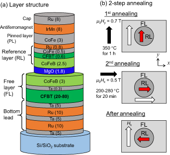
Figure 1. (a) Schematics of spin-valve TMR device and (b) two-step annealing process. The white and red arrows in (b) show the magnetization directions of FL and RL, respectively. The black arrows indicate the directions of magnetic field during annealing.
Download figure:
Standard image High-resolution imageR–H curves were measured using the conventional dc four-probe technique. The noise of the devices was measured in a triple-walled permalloy shield box with a Helmholtz coil that applies H to the devices. Bias voltage (Vb) was applied to the devices using a 1.5 V dry cell battery connected with a potentiometer in series to adjust Vb. The noise spectrum was measured by a Keysight 35670A dynamic signal analyzer after amplification by an ultralow noise preamplifier (NF Corporation, SA-200F3) with a gain of 40 dB. The microstructure of the films was investigated using scanning transmission electron microscopy (STEM) using a FEI Titan G2 80–200 microscope with a probe aberration corrector. The specimens for the STEM analysis were prepared using a FEI Helios G4-UX dual-beam system with the lift-out method. The distribution of the constituent elements was studied using energy-dispersive x-ray spectroscopy (EDS).
3. Results and discussion
3.1. Structure
Figures 2(a) and (b) show the bright-field (BF) STEM image and EDS map of the spin-valves with tCFBT = 20 nm annealed at 350 °C for 1 h. The CoFeB electrodes in the FL and RL have been crystallized with a [001] out-of-plane texture, whereas the CFBT layer remains amorphous as shown by the halo of the nano-beam electron diffraction pattern shown in the inset of figure 2(a). Relatively flat interfaces in the spin-valve structure are seen in figures 2(a) and (b). The spin-valve with tCFBT = 80 nm for the FL is shown in figures 2(c) and (d). The film interfaces are much rougher than those of the spin-valve with tCFBT = 20 nm, indicating that the surface roughness of the CFBT amorphous layer increases with increasing layer thickness.

Figure 2. Cross-sectional BF-STEM images and STEM-EDS maps of the spin-valves with (a, b) tCFBT = 20 nm, and (c, d) tCFBT = 80 nm, respectively.
Download figure:
Standard image High-resolution imageThe interface roughness between the CoFeB electrodes and the MgO barrier influences the TMR properties. The surface roughness of the test sample structure of substrate/Ta (2)/Ru (10)/Ta (2)/Ru (10)/Ta (5)/CFBT (tCFBT = 20–80)/Ta (0.3)/CoFeB (3)/MgO (2)/Ta (2) was measured by an atomic force microscope (AFM). Figures 3(a) and (b) show the AFM images for tCFBT = 20 nm for the as-deposited state and after annealing at 350 °C, respectively. The arithmetic average roughness (Ra) and the peak-to-valley (P–V) values were 0.17 nm and 1.9 nm for the as-deposited film and 0.25 nm and 2.7 nm for the annealed film, respectively. In addition to the increase in the roughness amplitude, the grain-like surface morphology became finer by annealing, which may be associated with the crystallization of CoFeB. As shown in figure 3(c), Ra increases monotonically as tCFBT increases, consistent with the STEM images (figure 2).
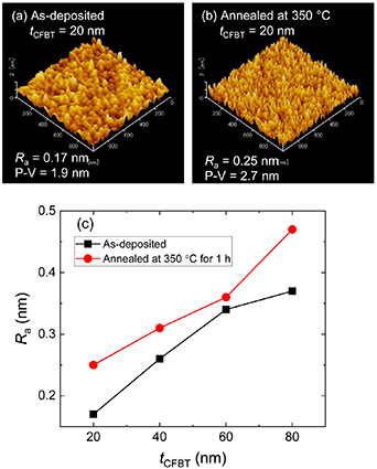
Figure 3. AFM images of the surface of the MgO barrier on the FL with tCFBT = 20 nm for (a) the as-deposited film and (b) the annealed film at 350 °C. (c) Surface roughness (Ra) vs. tCFBT.
Download figure:
Standard image High-resolution image3.2. Magnetic properties
Figure 4(a) shows the magnetization–magnetic field (M–H) curves of the spin-valve film with tCFBT = 20 nm after the first annealing at T1st = 350 °C under a magnetic field in the y-direction and after the second annealing at T2nd = 200 °C under a magnetic field in the x-direction. The magnetization is expressed by the product of saturation magnetization and thickness (4πMs t). The kinks of the M–H curves indicated by the arrows in figure 4(a) correspond to the effective pinning fields (Hpin) for the RL. By the first annealing, a pinning of the RL (μ0 Hpin = 35 mT) and magnetic anisotropy in the FL (μ0 Hk = 1.8 mT) were induced in the y-direction. By the second annealing, however, the initial pinning field was erased and reset in the x-direction with μ0 Hpin = 19 mT, while the anisotropy of the FL remains in the y-direction with a reduced strength of μ0 Hk = 1.2 mT. Thus, Hk of the FL is orthogonal to Hpin of the RL, which is often referred to as 'crossed-anisotropy configuration'.
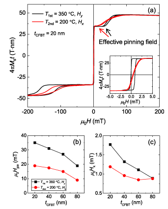
Figure 4. (a) Magnetization curves of the spin-valve film with tCFBT = 20 nm after first annealing at 350 °C and the second annealing at 200 °C. For the M-H measurements, H was applied in the pinning direction; y-direction for the first annealing and x-direction for the second annealing. Inset shows the M-H curves of the FL. Dependences of (b) effective pinning field (μ0 Hpin) and (c) anisotropy field of FL (μ0 Hk) on tCFBT.
Download figure:
Standard image High-resolution imageFigure 4(b) shows the dependence of μ0 Hpin on tCFBT. For both first and second annealing, μ0 Hpin is lowered with increasing tCFBT, which may be attributed to the larger film roughness as tCFBT increases, as shown in figures 2 and 3. For each tCFBT, μ0 Hpin is reduced by the second annealing at 200 °C compared to the values after the first annealing at 350 °C. This is because 200 °C is not the optimal annealing temperature for the highest exchange bias by the IrMn layers. Figure 4(c) shows the dependence of μ0 Hk on tCFBT. There is a trend that μ0 Hk decreases as tCFBT increases. For each tCFBT, μ0 Hk is reduced by the second annealing compared to the values after the first annealing.
3.3. TMR properties
Figure 5(a) shows the R–H transfer curves of the spin-valve devices with tCFBT = 20 nm annealed at various conditions, where R is expressed as the TMR ratio (=ΔR/RP). The resistance-area product in the parallel magnetization state (RAP) was ∼40 kΩ μm2. After the first annealing at 350 °C, the device shows a square-shaped R–Hy curve with a coercivity (μ0 Hc) of 0.5 mT and a small interlayer coupling field between the RL and the FL (μ0 Hint) of 0.3 mT. By annealing the film again at T2nd = 200 °C under a magnetic field in the x-direction, the crossed-anisotropy between the RL and the FL results in a linear R–Hx curve with a negligible μ0 Hc, which is suitable for magnetic field sensors. As T2nd increases to 250 °C and 280 °C, the R–Hx curves become hysteretic with larger μ0 Hc.
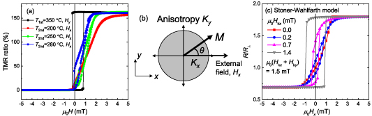
Figure 5. (a) R–H transfer curves of the spin-valve device with tCFBT = 20 nm annealed at various conditions. (b) Configuration of anisotropy, magnetization and external field for the Stoner–Wohlfarth modelling for the FL. (c) Calculated R–Hx curves for various Hkx values.
Download figure:
Standard image High-resolution imageThe change of the shape of the R–Hx curve for T2nd = 200 °C–280 °C shown in figure 5(a) is explained by assuming two magnetic anisotropy axes in the FL induced by the two-step annealing process. In the ideal two-step annealing process, the magnetic anisotropy of FL is induced only in the y-direction with an energy Ky by the first annealing, and the second annealing induces only an exchange bias pinning to PL and RL in the x-direction. However, the second annealing may induce an additional magnetic anisotropy in the FL in the x-direction (Kx ), as shown in figure 5(b). As the magnetization of the RL is strongly fixed within the external field range for the R–H measurements (μ0 Hext = ± 5 mT), we consider only the behavior of the magnetization of the FL by the Stoner–Wohlfarth model in a single-domain regime [16]. The total magnetic energy of the FL is expressed as

where M is the magnetization of the FL, θ is the angle between Hext and M. The anisotropy field Hk has a relationship of Hk = 2 K M−1
. Solving  under
under  gives θ that minimizes Etot for given Hkx
and Hky
. As shown in figure 4(c), Hky
induced by the first annealing decreased after the second annealing at T2nd = 200 °C; thus it is expected that Hky
decreases further and Hkx
increases for higher T2nd. For simplicity, we assume μ0(Hkx
+ Hky
) = 1.5 mT regardless of T2nd. Figure 5(c) shows calculated R–Hx
curves for variations of Hkx
using the angular dependence of TMR [17]:
gives θ that minimizes Etot for given Hkx
and Hky
. As shown in figure 4(c), Hky
induced by the first annealing decreased after the second annealing at T2nd = 200 °C; thus it is expected that Hky
decreases further and Hkx
increases for higher T2nd. For simplicity, we assume μ0(Hkx
+ Hky
) = 1.5 mT regardless of T2nd. Figure 5(c) shows calculated R–Hx
curves for variations of Hkx
using the angular dependence of TMR [17]:  , where
  and P are the resistance at θ = 90° and the tunneling spin polarization obtained by the Julliere's equation [18] (P2 ∼0.44 for a full TMR ratio of 160%), respectively. The FL offset field (Hint) is not included in these calculations. The R–Hx
curve for Hkx
= 0 shows a loop with Hc = 0 similar to the experimental result for T2nd = 200 °C. As Hkx
increases, the R–Hx
curves show hysteresis loops with nonzero Hc, which qualitatively agrees with the experiments for T2nd = 250 °C and 280 °C. Thus, the additional magnetic anisotropy induced in the FL in the x-direction explains the hysteretic R–Hx
loops for T2nd = 250 °C and 280 °C. Therefore, we conclude that T2nd = 200 °C is the optimal annealing temperature to obtain an appropriate crossed anisotropy in the TMR devices using the CFBT-based FL.
and P are the resistance at θ = 90° and the tunneling spin polarization obtained by the Julliere's equation [18] (P2 ∼0.44 for a full TMR ratio of 160%), respectively. The FL offset field (Hint) is not included in these calculations. The R–Hx
curve for Hkx
= 0 shows a loop with Hc = 0 similar to the experimental result for T2nd = 200 °C. As Hkx
increases, the R–Hx
curves show hysteresis loops with nonzero Hc, which qualitatively agrees with the experiments for T2nd = 250 °C and 280 °C. Thus, the additional magnetic anisotropy induced in the FL in the x-direction explains the hysteretic R–Hx
loops for T2nd = 250 °C and 280 °C. Therefore, we conclude that T2nd = 200 °C is the optimal annealing temperature to obtain an appropriate crossed anisotropy in the TMR devices using the CFBT-based FL.
Figure 6 shows the R–Hx curves with tCFBT = 20–80 nm after the two-step annealing at T1st = 350 °C and T2nd = 200 °C. All devices show a gradual change of R as Hx changes due to the crossed anisotropy. The anisotropy fields were similar for all tCFBT (2μ0 Hk ∼2.3 mT), while the TMR ratios were largely dependent on tCFBT. The lower TMR ratio for larger tCFBT may be explained by the larger film roughness as seen in figures 2 and 3. As shown in the inset of figure 6, the sensitivity defined by the TMR ratio/2μ0 Hk was ∼65%/mT for tCFBT = 20 and 40 nm and decreased for larger tCFBT. Hence, we focus on the TMR device with tCFBT = 20 nm for the following studies.
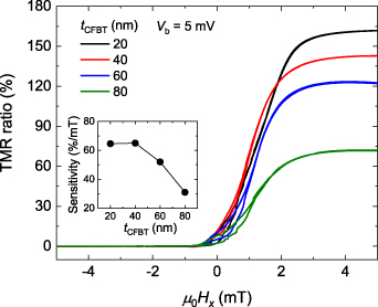
Figure 6. R–Hx curves for tCFBT = 20–80 nm after the two-step annealing (T1st = 350 °C and T2nd = 200 °C).
Download figure:
Standard image High-resolution image3.4. Low-frequency noise properties
We measured the noise spectra of a TMR sensor device with tCFBT = 20 nm patterned into a 50 μm diameter circle. Vb was fixed at 30 mV, where the positive sign of Vb corresponds to the flow of electrons from the FL to the RL. Figure 7(a) shows the R-Hx curve and the numerically obtained magnetic field sensitivity defined by 1/Rmin · (dR/dHx), where Rmin is the resistance in the P-state. The R–Hx curve shows a gradual change of R as Hx changes between μ0 Hx = 0 mT and +3 mT, due to the magnetization rotation of the FL. A maximum sensitivity of ∼70%/mT is obtained at μ0 Hx between +1.0 mT and +1.7 mT, where the R-Hx loop is almost nonhysteretic.

Figure 7. (a) R–Hx
curve of the TMR device with tCFBT = 20 nm measured at Vb = 30 mV and the corresponding sensitivity (1/ ·
· /
/ ). (b) Noise voltage spectra of the TMR device under various external magnetic fields. The noise of the pre-amplifier connected to a 33 Ω resistor, which is the same resistance as that of the TMR device at μ0
Hx
= +1 mT, is also shown. Magnetic field dependences of (c) noise voltage density at 10 Hz and the corresponding Hooge's noise parameter αH, and (d) detectivity at 10 Hz.
). (b) Noise voltage spectra of the TMR device under various external magnetic fields. The noise of the pre-amplifier connected to a 33 Ω resistor, which is the same resistance as that of the TMR device at μ0
Hx
= +1 mT, is also shown. Magnetic field dependences of (c) noise voltage density at 10 Hz and the corresponding Hooge's noise parameter αH, and (d) detectivity at 10 Hz.
Download figure:
Standard image High-resolution imageFigure 7(b) shows the noise voltage density  at μ0
Hx
= –5 (P-state), +1, +2 (intermediate magnetization states), and +5 mT (AP-state) for the same device biased at Vb = 30 mV. For these noise measurements, we first applied a magnetic field of μ0
Hx
= +5 mT to saturate the device in the AP-state, and then set it to the required magnetic field for the noise measurements. It was important to wait for a few minutes to equilibrate the magnetization state of the device before starting the noise measurements [19]. The noise of the pre-amplifier is also shown in figure 7(b), indicating that the electronics noise of the measurement setup is significantly smaller than the noise of the TMR device. The white noise level observed in the TMR device in f > a few kHz is larger in the AP-state than in the P-state because of the larger resistance in the AP-state. The value of
at μ0
Hx
= –5 (P-state), +1, +2 (intermediate magnetization states), and +5 mT (AP-state) for the same device biased at Vb = 30 mV. For these noise measurements, we first applied a magnetic field of μ0
Hx
= +5 mT to saturate the device in the AP-state, and then set it to the required magnetic field for the noise measurements. It was important to wait for a few minutes to equilibrate the magnetization state of the device before starting the noise measurements [19]. The noise of the pre-amplifier is also shown in figure 7(b), indicating that the electronics noise of the measurement setup is significantly smaller than the noise of the TMR device. The white noise level observed in the TMR device in f > a few kHz is larger in the AP-state than in the P-state because of the larger resistance in the AP-state. The value of  in the low-f regime (<1 kHz) is similar between the P-state and the AP-state, whereas the low-f noise in the intermediate magnetization states was much larger than those in the P- and AP-states, suggesting magnetic fluctuation dominates the 1/f noise in the intermediate magnetization states [20]. Figure 7(c) shows the magnetic field dependence of
  at f = 10 Hz and also the Hooge's noise parameters (αH) for μ0
Hx
= −2.0 mT, +1.0 mT, +2.0 mT and +4.0 mT was obtained by the relationship of
at f = 10 Hz and also the Hooge's noise parameters (αH) for μ0
Hx
= −2.0 mT, +1.0 mT, +2.0 mT and +4.0 mT was obtained by the relationship of  [21], where A is junction area (1962 μm2) and the thermal and pre-amplifer noises were subtracted from the measured
  . The high noise peaks observed at μ0
Hx
= –0.25 mT and +2.0 mT may be attributed to the fluctuation of magnetic domains nucleated in the MTJ when the FL starts to rotate from the P-state and the AP-state, respectively. The magnetic field dependence of detectivity D is shown in figure 7(d). The minimum D of ∼2 nT/
. The high noise peaks observed at μ0
Hx
= –0.25 mT and +2.0 mT may be attributed to the fluctuation of magnetic domains nucleated in the MTJ when the FL starts to rotate from the P-state and the AP-state, respectively. The magnetic field dependence of detectivity D is shown in figure 7(d). The minimum D of ∼2 nT/ at f = 10 Hz is obtained at μ0
H = +1.0 mT, where the sensivity and
at f = 10 Hz is obtained at μ0
H = +1.0 mT, where the sensivity and  are ∼70%/mT and ∼40 nV/
 , respectively.
Figure 8(a) shows the noise voltage spectra of the TMR device with tCFBT = 20 nm at various Vb. The magnetization state was set to the intermediate state by applying μ0
Hx
= +1 mT, where the minimum D was obtained at Vb = 30 mV (figure 7(d)). A typical 1/f noise characteristic was observed at Vb = 20 mV, 40 mV, 80 mV and 100 mV, where the Hooge's noise parameter was approximately constant αH ∼4 × 10⁻⁸
μm2. At Vb = 60 mV, however, a Lorentzian noise spectrum was observed, indicating random telegraph noise (RTN) with a center frequency of ∼700 Hz. The Vb-dependences of the noise spectra of the same device in the P- and AP-magnetization states were also measured (data not shown), where  increased linearly with increasing Vb between 20 mV and 100 mV with an approximately contant αH ∼1 × 10⁻⁸
μm2 in both magnetization states. No RTN was observed in either P- and AP-magnetization states. It is noteworthly that similar RTN was observed in other devices with the identical shape and size; however, the Vb where the RTN appeared and the center frequency of the RTN differed from device to device. In addition, the appearance of RTN was intermittent and did not necessarily reproduce in repeated measurements under nominaly idential conditions (see supplemental material (available online at stacks.iop.org/54/095002/mmedia)). Such characteristics of RTN in TMR devices have been reported previously [20–24] and explained by the thermally activated hopping of small magnetic domain(s) whose volume fraction is much smaller than 1% of the total volume of the FL [20, 24]. The strong Vb-dependence of the RTN may indicate that spin transfer torque plays a role in the activation process of the magnetic domain hopping, as discussed by Arakawa et al [24].
increased linearly with increasing Vb between 20 mV and 100 mV with an approximately contant αH ∼1 × 10⁻⁸
μm2 in both magnetization states. No RTN was observed in either P- and AP-magnetization states. It is noteworthly that similar RTN was observed in other devices with the identical shape and size; however, the Vb where the RTN appeared and the center frequency of the RTN differed from device to device. In addition, the appearance of RTN was intermittent and did not necessarily reproduce in repeated measurements under nominaly idential conditions (see supplemental material (available online at stacks.iop.org/54/095002/mmedia)). Such characteristics of RTN in TMR devices have been reported previously [20–24] and explained by the thermally activated hopping of small magnetic domain(s) whose volume fraction is much smaller than 1% of the total volume of the FL [20, 24]. The strong Vb-dependence of the RTN may indicate that spin transfer torque plays a role in the activation process of the magnetic domain hopping, as discussed by Arakawa et al [24].
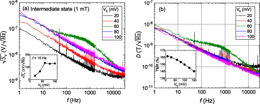
Figure 8. Vb dependences of (a) noise voltage density and (b) detectivity (D) of the TMR device with tCFBT = 20 nm patterned to a 50 μm circular shape.
Download figure:
Standard image High-resolution imageThe value of  at f = 10 Hz is shown in the inset of figure 8(a).
  increases approximately in proportion to Vb between 20 mV and 80 mV, except at 60 mV where the RTN appears. Figure 8(b) shows the f-dependence of D of the same device. The depepdence of the TMR ratio on Vb shown in the inset of figure 8(b) was used to calculate D. As
  scales linearly with Vb for between 20 mV and 80 mV except for 60 mV, almost constant D of 2.2 nT/
 at 10 Hz was obtained regardless of Vb.
We also investigated the dependence of  on the junction area A for the TMR device with tCFBT = 20 nm. Note that the device was patterned into circular shapes with diameters ranging from 5 μm to 50 μm and the Ar ion milling was performed down to the MgO tunnel barrier, thus A defines the area of PL, RL and MgO barrier. The FL was patterned to a much larger area (100 μm × 400 μm). As shown in figure 9,
  shows a relationship of
  ∝ 1/
∝ 1/ , indicating an approximately constant αH of 4 × 10⁻⁸
μm2 from the relationship of
, indicating an approximately constant αH of 4 × 10⁻⁸
μm2 from the relationship of  , also as reported previously in a NiFeCo/Al2O3/CoFe MTJ [25]. Since the TMR ratio and its Vb-dependence are independence of A, a constant sensitivity is obtained regardless of A. Thus, smaller D is obtained as A increases.

Figure 9. Dependence of noise voltage density at 10 Hz on the area of the MTJ with tCFBT = 20 nm.
Download figure:
Standard image High-resolution image
We have obtained linear R–H response curves with negligibleHc using the TMR devices with a CFBT (20 nm)/Ta (0.3 nm)/CoFeB (3 nm)-FL under an optimal two-step annealing condition (T1st = 350 °C and T2nd = 200 °C), which is suitable for magnetic field sensor applications. The properties of the CFBT-based TMR sensor are summarized in table 1 in comparison with reported TMR sensors with NiFe and CoFeSiB soft magnetic layers. The noise voltage density  at 10 Hz is normalized by dividing by Vb because
  Note that these data are for single devices without array structure or integration with magnetic flux concentrator. Fujiwara et al reported a very high sensitivity of up to 253%/mT using a NiFe (70 nm)/Ru (0.9 nm)/CoFeB (3 nm)-FL with a small μ0
Hk of 0.3 mT by a two-step annealing [10, 26]. For these sensors, only the noise level in the P-state has been reported to be
Note that these data are for single devices without array structure or integration with magnetic flux concentrator. Fujiwara et al reported a very high sensitivity of up to 253%/mT using a NiFe (70 nm)/Ru (0.9 nm)/CoFeB (3 nm)-FL with a small μ0
Hk of 0.3 mT by a two-step annealing [10, 26]. For these sensors, only the noise level in the P-state has been reported to be  ∼3.3 nV/
 /mV, which is much larger than that of our device of ∼0.7 nV/
 /mV in P-state. In addition, our device shows a smaller D than those reported for the TMR sensors with NiFe-based FLs [13, 27], which is explained by a higher sensitivity and a lower noise in our device with the CFBT-based FL.
Table 1. Properties of TMR single devices with CFBT (this work), NiFe and CoFeSiB soft magnetic layers. Tan: annealing temperature (the numbers in parentheses are Tan of the second annealing for two-step annealing process), A: junction area, μ0
Hk: magnetic anisotropy field of FL, S: sensitivity,  : noise voltage density normalized by bias voltage, αH: Hooge's noise parameter, D: detectivity. 'Hbias' and 'soft pin' denote external bias field and softly-pinned exchange bias for Hk of FL.
| Soft magnetic layer | Tan (°C) | A (μm2) | μ0 Hk (mT) | TMR ratio (%) | S (%/mT) |
 at 10 Hz
(nV/ at 10 Hz
(nV/ /mV) /mV) | αH (μm2) |
D (nT/ )
at 10 Hz )
at 10 Hz | Reference |
|---|---|---|---|---|---|---|---|---|---|
| CoFeBTa | 350 (200) | 1962 | 1.2 | 160 | 70 | 1.3 0.7 (P-state) | 4 × 10⁻⁸ | 2.2 | This work |
| Ni80Fe20 | 325 (300) | 3200 | 0.3 | 150 | 253 | 3.3 (P-state) | 3.3 × 10⁻⁷ (P-state) | [10, 12] | |
| 325 | 300 | 1.0 (Hbias) | 170 | 12.8 | [13] | ||||
| 330 | 2463 | 4.2 (soft pin) | 191 | 22.7 | 2.9 | 2.1 × 10⁻⁷ | 16.1 | [27] | |
| CoFeSiB | 375 (300) | 0.28 | 228 | 400 | [11] | ||||
| 325 | 300 | 1.0 (Hbias) | 200 | 4 × 10⁻⁹ | 4.5 | [13] |
The TMR sensors with a CoFeSiB-based FL have been reported to show a very high sensitivity of 400%/mT due to a small μ0 Hk of 0.28 mT although the noise properties have not been discussed in the paper by Kato et al [11]. Huang et al reported a smaller αH, but a larger D using sensors with a CoFeSiB-based FL, where the FL is biased by external magnetic field [13], than those of our sensors. However, a direct comparison between the performances of our sensors with the CFBT-based FL and those with the CoFeSiB-based FL is not possible because of the different techniques for Hk of FL; i.e. by two-step annealing vs. by external magnetic field. Thus, we need a side-by-side comparison for benchmarking these soft magnetic layers under the same sample structures and measurement conditions.
4. Summary and conclusions
We developed CoFeB/MgO/CoFeB-based TMR sensor devices incorporating an amorphous CFBT soft magnetic layer in the FL. STEM observations confirmed that the CFBT layer remained amorphous even after annealing at 350 °C, while the CoFeB electrodes in contact with the MgO tunnel barrier have been crystallized with a [001]-texture. The interface roughness between the CoFeB electrodes and the MgO tunnel barrier increased with increasing tCFBT in the FL, by which the TMR ratio decreased as tCFBT increased. Linear R-H response curves with negligible Hc were obtained by a two-step annealing process at particular temperatures. The first annealing at T1st = 350 °C induces a magnetic anisotropy in the FL in the y-direction and the second annealing at T2nd = 200 °C sets the exchange bias pinning on the PL/RL in the x-direction. Higher T2nd resulted in hysteretic R-H curves, which are explained by additional magnetic anisotropy induced in the x-direction. The devices with a CFBT (20 nm)/Ta (0.3 nm)/CoFeB (3 nm)-FL showed a TMR ratio of 160%, sensitivity of 70%/mT and D ∼2 nT/ at 10 Hz for a junction size of 50 μm in diameter. 1/f noise dominated the sensor noise in frequencies below 10 kHz and its voltage density was higher in the intermediate magnetization state than in the P- and AP-states. RTN was observed in the intermediate magnetization state only at a particular bias voltage (Vb). The 1/f noise level increased in proportion to Vb and decreased in proportion to the square root of juncion area (A). The Hooge's noise parameter was αH ∼4 × 10⁻⁸
μm2, independent of Vbias and A. This study indicates that CFBT is a suitable soft magnetic layer for TMR sensors, by which a lower noise level than those of previously reported TMR sensors with NiFe soft magnetic layers was demonstrated.
at 10 Hz for a junction size of 50 μm in diameter. 1/f noise dominated the sensor noise in frequencies below 10 kHz and its voltage density was higher in the intermediate magnetization state than in the P- and AP-states. RTN was observed in the intermediate magnetization state only at a particular bias voltage (Vb). The 1/f noise level increased in proportion to Vb and decreased in proportion to the square root of juncion area (A). The Hooge's noise parameter was αH ∼4 × 10⁻⁸
μm2, independent of Vbias and A. This study indicates that CFBT is a suitable soft magnetic layer for TMR sensors, by which a lower noise level than those of previously reported TMR sensors with NiFe soft magnetic layers was demonstrated.
Nevertheless, the value of D of the present TMR sensor (∼2 nT/ at 10 Hz) is much larger than that required for the detection of a biomagnetic field (∼1 pT/
 in low frequency regime). To achieve such high magnetic field resolution, efforts in terms of both increasing the sensitivity and reducing the noise of the TMR sensor are required; e.g. by (1) integration with magnetic flux concentrator [27–29], (2) reducing the intrinsic noise of the TMR device by new materials, (3) array, by connecting many devices in serial and parallel [30, 31], (4) AC modulation to shift the sensor's operating frequency to a >1 kHz regime where thermal noise dominates the noise of the sensor [32, 33].
Acknowledgments
This work was partly supported by JSPS KAKENHI Grant Numbers 17H06152 and 20K04588.