

Abstract
In this paper, the growth of orthorhombic and monoclinic (AlxGa1 − x)2O3 thin films on (00.1) Al2O3 by tin-assisted pulsed laser deposition is investigated as a function of oxygen pressure p(O2) and substrate temperature  . For certain growth conditions, defined by
  ≥ 580°C and p(O2) ≤ 0.016 mbar, the orthorhombic κ-polymorph is stabilized. For
  = 540°C and p(O2) ≤ 0.016 mbar, the κ-, and the β-, as well as the spinel γ-polymorph coexist, as illustrated by XRD 2θ-ω-scans. Further employed growth parameters result in thin films with a monoclinic β-gallia structure. For all polymorphs, p(O2) and
  affect the formation and desorption of volatile suboxides, and thereby the growth rate and the cation composition. For example, low oxygen pressures lead to low growth rates and enhanced Al incorporation. This facilitates the structural engineering of polymorphic, ternary (Al,Ga)2O3 via selection of the relevant process parameters. Transmission electron microscopy (TEM) studies of a κ - (Al0.13Ga0.87)2O3 thin film reveal a more complex picture compared to that derived from x-ray diffraction measurements. Furthermore, this study presents the possibility of controlling the phase formation, as well as the Al-content, of thin films based on the choice of their growth conditions.
Export citation and abstract BibTeX RIS

Original content from this work may be used under the terms of the Creative Commons Attribution 4.0 license. Any further distribution of this work must maintain attribution to the author(s) and the title of the work, journal citation and DOI.
1. Introduction
Gallium oxide is the focus of research interest, as, given its outstanding properties, such as a wide bandgap, high electrical breakdown field [1] of 8 MVcm−1 and large Baliga's figure of merit it is considered to be suitable for a variety of applications, including deep-UV photo detectors [2], gas sensors [3], high power rectifiers, and transistors [4–9]. The band gap ranges between 4.6 eV and 5.3 eV, depending on the respective polymorph, and can be reduced or enlarged by alloying with In2O3 or Al2O3 to expand the range of possible applications [10]. To date, most of the published studies have dealt with the thermodynamically stable monoclinic β-polymorph, but in recent years, the meta-stable orthorhombic κ-polymorph has garnered increasing interest, owing to its predicted large spontaneous polarization of 23 µC/cm2 along its c-axis [11]. Extensive studies addressing this polymorph will be required to potentially realize high power and optical devices [12]. Cora et al [13] studied the crystal structure of this polymorph in detail, assigning it to the space group Pna21, with two distinct cation sites, having a ratio of 1:3 of tetrahedrally and octahedrally coordinated Ga sites. In addition, they compared the orthorhombic with the hexagonal crystal structures, identifying the orthorhombic κ-Ga2O3 as a coordinated subgroup of the hexagonal  -phase [13].
Binary orthorhombic Ga2O3 can be realized by a variety of growth techniques, such as halide vapor phase epitaxy HVPE[14, 15], atomic layer deposition[16] (ALD), metal organic chemical vapor deposition [13, 17–21] (MOCVD), mist CVD [22, 23], and plasma-assisted [24] or tin-assisted MBE [25], as well as tin-assisted pulsed laser deposition [26, 27] (PLD). In contrast, ternary alloys containing Al or In have so far only been realized by tin-assisted PLD [28–31] (PLD) on c-sapphire and κ-Ga2O3 templates as well as by mist CVD [32, 33] on c-plane AlN templates. With regard to PLD, a certain tin supply is necessary in addition to adequate growth conditions (growth temperature and pressure) in order to stabilize the orthorhombic phase [27]. To date, the highest reported Al content has been x = 0.46 for κ - (Al,Ga)2O3 on (00.1)Al2O3 [31] which can be enhanced up to x = 0.65 by employing an additional κ-Ga2O3 thin film template [29]. Kneiß et al have described the growth of binary κ-Ga2O3 using tin, which is not incorporated into the thin film, but serves as a surfactant [27, 31].
For binary β-Ga2O3 thin films, decreasing  or increasing
  (by PLD) or metal-rich regimes (by MBE) leads to decreasing growth rates, caused by the formation and subsequent desorption of volatile Ga2O suboxides [34–37]. For β-(Al,Ga)2O3 thin films, the same behaviour has been observed, but with one special feature: a change of the Al/Ga ratio in the thin films [38–40], which is due to the favored incorporation of Al into the layer. In contrast, for β-(In,Ga)2O3 thin films, the incorporation of Ga atoms is favored, leading to lower In-contents in the case of growth in oxygen-poor conditions [41]. Since growth parameters have such a significant impact on the material properties of β-Ga2O3-based thin films, a systematic study of the influence of these growth parameters for the less investigated orthorhombic phase is mandatory. In this paper, we present a detailed structural characterization on the nanoscale, in conjunction with a detailed description of the phase formation of (Al,Ga)2O3 thin films on c-plane sapphire, as well as the influence of
  and p(O2) on this. Moreover, we illustrate the effect of the formation of volatile suboxides on cation incorporation, and therefore on the change of the cation composition in the layer and the growth rate of the thin film.
For this purpose, we deposited (Al,Ga)2O3 thin films on c-sapphire substrates under various growth conditions. The experiments reveal that orthorhombic (Al,Ga)2O3 can be stabilized only under certain growth conditions. This requires growth temperatures above 540°C and oxygen pressures below 0.024 mbar, except for the highest investigated growth temperature of 670°C, where p(O2) = 0.024 mbar still leads to κ-phase thin films. For  = 540°C and p(O2) ≤ 0.016 mbar, as well as for 620°C and 0.024 mbar, the coexistence of κ-, β- and γ-polymorphs is observed. Other growth parameters can lead to monoclinic thin films. The crystal structure of one κ - (Al0.13Ga0.87)2O3 thin film and one (Al0.11Ga0.89)2O3 thin film exhibiting phase separation (κ and β + γ) are investigated in detail, using TEM measurements.
2. Results and discussion
2.1. Crystal structure
The influence of growth parameters on the formation of κ - (AlxGa1 − x)2O3 thin films was analyzed by varying  and p(O2) during PLD growth, utilizing the same ceramic PLD target for all prepared samples. The thin films were also examined under x-ray diffraction, revealing the crystal structure to be monoclinic, orthorhombic, or a coexistence of both. In figure 1, representative 2θ-ω scans (2θ = 15–65°) of (AlxGa1 − x)2O3 thin films are depicted, revealing characteristic reflection peaks, which can be assigned either to the β- or the κ-phase. Peaks corresponding to both phases are present for samples exhibiting phase separation. The growth conditions, Al-content and identified phase of these (AlxGa1 − x)2O3 thin films are presented in table 1. These samples will be referred to as samples A, B, and C below.

Figure 1. XRD patterns of an orthorhombic κ- (A), a monoclinic β-(AlxGa1 − x)2O3 thin film (C), and a thin film exhibiting a coexistence of both (B). The growth directions of the respective samples are labeled in red for the monoclinic, and blue for the orthorhombic lattice planes. The shoulders highlighted by the arrow can be assigned either to (-313) or (333)
 lattice planes. The peak positions were assigned according to JCPDS card nos. 76-0573, 20-0426 and 11-0342. The reflection peak visible at 41.68° can be assigned to the (00.6) Al2O3 lattice plane (JCPDS PDF card no. 82-1399).
Download figure:
Standard image High-resolution imageTable 1. Growth temperature  , oxygen pressure p(O2), measured Al content x by EDX, and polymorph for samples A, B and C.
| label |  (°C) (°C) | p(O2) (mbar) | x | polymorph |
|---|---|---|---|---|
| A | 620 | 0.002 | 0.13 | κ |
| B | 540 | 0.001 | 0.11 | phase separation |
| C | 500 | 0.002 | 0.10 | β |
At the bottom of figure 1, the XRD pattern of sample C, a polycrystalline β - (AlxGa1 − x)2O3 thin film grown at 500°C and 0.002 mbar, reveals the growth along the (-201) n lattice plane. This is indicated by the lattice plane reflection peaks observable at 2θ = 18.82°, 38.21°, and 59.10°. The growth along the (-201) lattice plane on c-plane sapphire has already been reported several times in relation to β - (AlxGa1 − x)2O3 [39, 40, 42, 43]. Aside from the (-201) orientation, two additional orientations of the β-phase are visible in the scan: the (-401)
 at 2θ = 30.13°, and the (-601)
 at 2θ = 44.26°. The XRD pattern of sample A (top panel of figure 1), which was grown at 620°C and 0.002 mbar, reveals reflection peaks at 2θ = 19.26°, 39.03° and 60.11°, which can be assigned to the (002) n lattice planes of κ - (AlxGa1 − x)2O3. These reflection peaks occur at slightly higher angles compared to those of the β-thin film described above, which is typical for binary κ-Ga2O3 [27], as well as its ternary alloys (κ - (In,Ga,Al)2O3) [28–31]. The thin film B, shown in the middle of figure 1, was grown at 540°C and 0.001 mbar. The XRD pattern for this sample contains all previously described peaks, indicating phase separation. In addition, a peak shoulder appearing at 2θ = 58.02° is observed for B and C (marked with an arrow), which cannot be unambiguously assigned to a lattice plane reflection. One possible explanation for this is the presence of reflections at the monoclinic (-313)
 and the cubic (333)
 lattice plane, or an convolution of both. The c-plane sapphire (00.6) lattice plane reflection peak appears for all samples at 41.68°. Small peaks at 20.4° and 29.0° can also be observed (e.g. for sample A), emanating from the so-called Umweganregung (x-ray double diffraction) of the substrate. Such an Umweganregung is only observable under certain φ rotations, and may therefore occur in some samples [44]. Further visible reflection peaks are due to the K
 (35.2°, 53.9°) or the tungsten L
 (37.4°) spectral lines.
In order to compare the crystalline quality of β- and κ - (Al,Ga)2O3, the FWHMs of samples A and B were determined for the (004) and (-402)
 reflection peaks. For the (-402)
 reflection, the FWHM amounts to 0.258°, and for (004)
 it is 0.120°, exhibiting a lower broadening, and therefore representing a higher crystalline quality. The thin film thickness does not play a role, since the thickness of the samples is similar (470 nm for sample A, and 510 nm for C). The small differences in thin film thickness are caused by the different growth temperatures and the associated desorption of volatile suboxides [36, 37].
Since the oxygen pressures during growth of the three samples were nearly the same (0.001 or 0.002 mbar, respectively), the difference in growth temperature is accountable for the crystallization of the different phases seen here. Moreover, the growth temperature influences the incorporation of Al into the layers, which increases with increasing  . Note that the Al content present in the target is approximately 8.8 at.%. In the layers, values of 10 to 13 at.% were detected (see table 1). A detailed description of this phenomenon maycan be found in the section Phase Control. In the next section we want to focus on an atomically resolved description of the orthorhombic thin film (sample A) and the thin film exhibiting phase separation (sample B).
2.2. Growth
TEM investigations were performed for samples A and B and the cross-sectional TEM bright field images are shown in figure 2(a) and (b), respectively. In both layers, two phases of different morphologies can be clearly distinguished: a speckle-contrast region starting from the interface, indicating a highly granular structure, and on top of that a phase with vertically aligned features, indicating columnar-like domains. Selected area electron diffraction (SAED) was performed for each of these regions to identify the crystal structure and the growth orientations. This measurement was performed for two zone axis orientations of the sapphire substrate, [11 0] and [1
 00], for which the data are presented in figure 2(c). With regard to electron diffraction simulations [45], the red circled region is identified as a coexistence of the monoclinic β- and the cubic γ-phase. The γ-Ga2O3 phase has a cation-deficient spinel structure (
 ) described in detail by Playford et al [46], and similar to that of γ-Al2O3. The blue circled region can be identified as the orthorhombic κ-structure in both samples, as shown in figure 2(c). The SAED patterns of the κ- and β + γ-regions of sample A look the same as those presented for sample B. The domain boundaries between the β + γ-part and the κ-phase extend diagonally through the layer. This suggests that the κ-phase starts to nucleate as islands in certain positions, probably due to Sn accumulations, then grows at a higher growth rate than the β + γ-phase until the latter is overgrown. The composition in both phases is the same, as confirmed by STEM-EDXS measurements of the TEM sample. A STEM-EDXS spectrum can be found in the supplemental material (stacks.iop.org/JPD/53/485105/mmedia).

Figure 2. TEM bright field overview images of (AlxGa1 − x)2O3 layers grown at (a)  = 620°C and p(O2) = 0.002 mbar and (b)
  = 540°C and p(O2) = 0.001 mbar, corresponding respectively to samples A and B, shown in Fig 1. (c) Selected area electron diffraction (SAED, inverted contrast) in two zone axis orientations of the sapphire substrate in the areas indicated by red and blue circle in (b). We note that the streaky horizontal features in the SAED patterns of the κ-phase (blue) are probably caused by the short domain width in this direction, which breaks the periodicity.
Download figure:
Standard image High-resolution imageThe different phases are investigated in greater detail via Scanning TEM (STEM) imaging. Figure 3(a) shows a STEM image, taken close to the interface in sample B, and including the sapphire substrate and regions with β + γ- and κ-phase. The κ-phase is shown at higher magnification in figure 3(b), where we see that it is growing in narrow columnar domains of a few nanometers in width. The structure exhibits vertical lines of defects, extending through the structure (positions indicated by the white arrows), which are indicative of the vertical domain boundaries. The atomically resolved structure of the κ-phase is displayed in figure 3(c)II, and fits well to the atomic model superimposed on the experimental image. Ga columns appear bright in these images, while oxygen atoms are too light to produce a visible contrast. The domains are 60° rotated in plane with respect to each other, and the epitaxial relationships are (001) (00.1)
 and [010]
 , [310]
 [1
[1 00]
00] and [100]
 , [110]
 [11
[11 0]
0] .
.

Figure 3. (a) STEM image of an area in sample B ( = 620°C and p(O2) = 0.002 mbar) showing the substrate, the β+γ-mix phase, and the κ-phase. (b) Higher magnification image of the blue area in (a), showing a defective κ-structure due to many vertical domain boundaries. (c) STEM images of areas II, III and IV in (a), showing the atomically resolved pattern of the κ-, α+γ-, and β-structures, respectively, with the atomic models superimposed (blue & green: 6-fold and 4-fold coordinated Ga respectively, red: O) For the cation-deficient γ-phase, only those cations with the highest occupancy are shown in the model structure.
Download figure:
Standard image High-resolution imageA high magnification image of the interface region (shown in figure 3(c) III) actually reveals the presence of a fourth phase, namely α. It grows pseudomorphically for 3-4 monolayers on the sapphire substrate, with the same crystal structure. This phase is not detectable in XRD, because the layer is buried and too thin. The formation of this α-interlayer has already been shown to be typical for Ga2O3 layer growth on sapphire [47].
Close to the interface, small grains (measuring only a few nm) of β- and γ-phase are mixed randomly, while at larger thicknesses the grains grow larger and the β-phase is dominant. Figure 3(c) shows area scans for γ- and a β-phase grains where the structures can be fitted to the stick-and-ball models. Despite these small grains, both β- and γ-phases exhibit an epitaxial relationship with respect to the sapphire. For the out-of-plane orientation, (-201) (00.1)
 and (111)
 (00.1)
 was found. The spacings of these planes are very close to each other in value (d((-201)
 ) = 4.70 Å and d((111)
 ) = 4.75 Å), therefore the phases can hardly be distinguished in the XRD patterns. The in-plane relationship for the γ-phase is [1
 0]
0] [1
[1 00]
00] . The β-grains grow in different orientations, rotated in-plane by 60° with respect to each other, according to [010]
 or [132]
 [1
[1 00]
00] . Since this polycrystalline interlayer is only a few 10 nm thick in sample A, it implies that these grains are even smaller, which could explain the x-ray amorphous behavior of this layer. The formation of the approximately 20–30 nm small and wavy interlayer can be explained by the PLD approach employed here. During the first laser pulses an insufficient amount of tin is ablated, and the required liquid tin layer cannot form instantaneously. Only when this tin layer has formed can the growth of the orthorhombic phase begin.
Investigations of the surface morphology of samples A and C show similar results to comparable samples published previously [29, 31]. Therefore, only the surface morphology of sample B is presented below. AFM measurements show a surface consisting of 3D islands, which has a root mean square surface roughnesses of 8.6 nm. Figure 4(a) shows a 5 × 5 µm2 surface scan, depicting 3D islands, 200–400 nm in diameter. By considering the cross-sectional view, presented in figure 4(b), it can be established that the higher parts of the thin films can be allocated to the orthorhombic phase. The higher growth rates of the κ-phase, compared with those of the β-phase, leads to an overgrowth of the β + γ-part. If the thin film growth were to continue, e.g. by a higher pulse number from the PLD, it may be assumed that the κ-phase proportion would grow further in lateral size and finally overgrow the β + γ-part completely. Such complete overgrowth is visible in figure 2(a) for the κ - (Al,Ga)2O3 thin film.
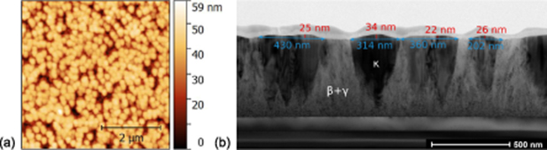
Figure 4. (a) 5× 5 µm2 AFM scan and (b) TEM cross-sectional view of sample B.
Download figure:
Standard image High-resolution image2.3. Phase control
In addition to the aforementioned samples, thin films were deposited under several growth conditions (various combinations of p(O2) and  ) and investigated via XRD to determine their crystal structure, by EDX to define their cation composition, and by spectroscopic ellipsometry to examine their growth rates. Note that the ceramic target employed here consists of Ga2O3 doped with 8.8 at.% Al2O3. Although TEM images show that the phase distribution is more complicated, below, we will focus only on phases with a high volume fraction, as identified by XRD.
The growth conditions, such as oxygen pressure and substrate temperature, were selected in the ranges of 3× 10⁻⁴ mbar ≤ p(O2) ≤ 0.024 mbar, and 450°C ≤  ≤ 670°C. Every sample was measured using XRD to determine the respective polymorph. The sample series for p(O2) = 0.000 3 mbar is depicted in figure 5, showing a change in the crystal structure, dependent on
  . For temperatures from 670 to 580°C, the κ-phase forms, for 540°C we obtain a mixture of the β + γ- and κ-phases, and for 500-450°C, the β-phase forms. The XRD spectra for the remaining oxygen pressures and growth temperatures can be found in the supplemental material. The evaluation of these detected crystal structures revealed defined growth conditions, among them the κ-modification forms presented in figure 6(a). These specific growth conditions are required for the given amount of tin in the target, due to the surfactant-mediated growth, where a liquid tin layer forms on top of the thin film, inducing the κ-growth below. The tin will not be incorporated into the layer, and desorbs, or rather accumulates at the top, as demonstrated for κ-(Al,Ga)2O3 [31].

Figure 5. XRD 2θ-ω scans of (AlxGa1 − x)2O3 thin films deposited at p(O2) = 0.000 3 mbar and various growth temperatures as labeled. The growth directions of the orthorhombic κ- and monoclinic β-samples are indicated in the graphs.
Download figure:
Standard image High-resolution image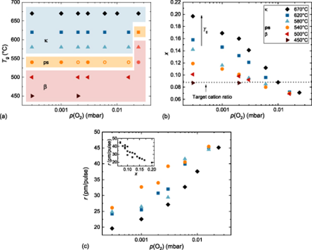
Figure 6. (a) Influence of the growth conditions (p(O2) &  ) on the formation of orthorhombic κ- and monoclinic β-(AlxGa1 − x)2O3. The different line widths of the sample exhibiting phase separation (ps) indicate the intensity of the observable β-reflection peaks: a larger width means a more intense peak. (b) Al content x by EDX as a function of the oxygen pressure for the different polymorphs and growth temperatures, as labeled. The dotted line denotes the cation ratio from the target. (c) Growth rate r vs dependence on p(O2). The inset shows the dependence on the Al-content.
Download figure:
Standard image High-resolution image
In the oxygen rich regime of 0.024 mbar, and at growth temperatures between 540°C and 580°C, the tin atoms completely oxidize, a liquid tin layer does not form, and hence the formation of the κ-phase is suppressed. To determine the point of transition from the β- to the κ-phase more accurately, thin films were grown between 540°C and 620°C instead of at an oxygen pressure of 0.01 mbar at 0.016 mbar. For temperatures below 500°C, surface-mediated growth cannot be observed, such that the monoclinic polymorph forms across the whole examined pressure range. In a narrow growth window of  = 540°C and 3× 10⁻⁴ mbar ≤ p(O2) ≤ 0.016 mbar, as well as for 620°C and 0.024 mbar, both phases coexist, as described in the previous section. Conceivably, the creation of the liquid tin layer is insufficient and/or small in this growth regime. The cation composition was investigated by means of EDX measurements, and is depicted as a function of the Al content x in figure 6(b). As reported for β - (AlxGa1 − x)2O3 thin films [40], x increases with decreasing oxygen pressure and/or increasing growth temperature up to 2.25 times the amount of material actually offered in the target. In monoclinic thin films, volatile Ga2O suboxides form at the layer surface, and subsequently desorb. As a result, the Ga2O species is preferentially formed, due to the lower dissociation energy of the Ga-O bond compared to the Al-O bond. The higher the oxygen deficit (low p(O2)) and/or the higher
  , the more suboxides form and desorb, leading to a higher Al concentration in the thin film. Since for the κ-polymorph grown by PLD, surface-mediated growth was reported [27, 31], the desorption process should be influenced by the existence of the liquid tin layer on the thin film's surface. The exact growth and desorption mechanism should be the focus of future research projects. However, the Al incorporation for the κ-, β- and the samples exhibiting phase separation is presented in figure 6(b) in relation to its dependence on p(O2) and
  . Regarding the
  series, it is observable that the desorption process diminishes for decreasing
  . The growth pressure, where a stoichiometric target-to-layer cation transfer can be monitored, shifts continuously to lower p(O2). The stoichiometric cation transfer is x = 0.088, and is marked in figure 6(b). For
  = 670°C, this point is reached at p(O2) = 0.01 mbar, for 580°C at around 0.006 mbar, for 540°C and 500°C at 0.003 mbar, and for 450°C a stoichiometric cation transfer was observed between 3 × 10⁻⁴ and 0.002 mbar. Since the Al content of the samples grown at 500°C and 450°C shows only a small change or no change in x, no additional thin films were grown. In an oxygen rich regime, p(O2) ≥ 0.016 mbar, the cation transfer of Al is x = 0.07, because the lighter Al ions are more widely scattered than the heavier Ga ions. For high p(O2), x remains constant and increases are no longer as visible at 620°C, 580°C, and 500°C, indicating that the formation of volatile Ga2O is suppressed [36, 37]. Nevertheless, the surface-mediated growth reduces the desorption process compared to the monoclinic phase. To demonstrate this, the κ - (AlxGa1 − x)2O3 thin films grown at 670°C can be compared with β - (AlxGa1 − x)2O3 thin films published before [40]. The target used for both sample series consists of an admixture of 8.8 at.% Al2O3, and the samples are grown at 670°C and at various oxygen pressures. The monoclinic thin films show systematically higher x for all oxygen pressures. Another indication of the lower incorporation of Ga into the layer due to desorption of volatile Ga2O is a decrease in the growth rate r, which was determined by spectroscopic ellipsometry and presented in figure 6(c). The graph shows a dependency on the growth conditions. With decreasing p(O2) and/or increasing
  , the growth rate also decreases. The behaviour of r is in accordance with an increased desorption of volatile Ga2O, which is indicated by the inset of figure 6(c), where r is plotted against x: r decreases approximately linearly with increasing x. The lowest r is about 19 pm/pulse for the lowest investigated oxygen pressure (3 × 10⁻⁴ mbar), the highest temperature (670°C) and the lowest Ga content (1-x = 0.8). For the highest investigated oxygen pressures (0.016 mbar and 0.024 mbar), the growth rates seem to saturate for all investigated
  between 45 - 46.5 pm/pulse. Interestingly, this is the growth region where fewer Al atoms are present, as they were incorporated into the thin film, suggesting that deposition kinematics, such as scattering, play a minor role compared to the forming and desorption of volatile suboxides.
3. Conclusion
In this work, (Al,Ga)2O3 thin films were deposited under various growth conditions, leading to the crystallization of orthorhombic or monoclinic polymorphs, or a coexistence of both, in addition to cubic defect spinel phases. This allows for the dedicated preparation of a desired crystal structure by means of selecting the relevant growth parameters. The orthorhombic structure forms under higher growth temperatures, and the monoclinic structure at high oxygen pressures and/or low growth temperatures. A coexistence of these phases and the γ-phase can only be observed for p(O2) ≤ 0.016 mbar and  = 540°C, as well as for 0.024 mbar and 620°C. Furthermore, we have shown that under low p(O2) and/or high
  , volatile suboxides form and desorb, which leads systematically to increasing Al contents and decreasing growth rates. Here, surfactant-mediated growth is suggested to be the growth mechanism for κ-(Al,Ga)2O3. Volatile suboxides are formed independent of the polymorph; it seems that the liquid tin layer reduces this process to some extent, as indicated by the cation composition evolution. For a sample grown at
  = 620°C and p(O2) = 0.002 mbar, TEM results reveal that a 3-4 monolayer thick α - (AlxGa1 − x)2O3 layer grew first on the substrate, with a thin polycrystalline β + γ - (AlxGa1 − x)2O3 layer and the κ - (AlxGa1 − x)2O3 thin film on top. Neither α - nor β + γ - layers were observed by x-ray diffraction measurements for this sample. Furthermore, TEM and AFM measurements of a sample grown in a phase mixture have been demonstrated. The side-by-side growth of the κ - and β + γ - phase could be caused by an insufficient and/or a small liquid tin layer on top of the sample.
4. Experimental
The (AlxGa1 − x)2O3 thin films presented here were grown by PLD on 10 × 10 mm2 sized c-sapphire substrates at various growth temperatures, ranging between 550°C and 670°C, as well as at oxygen partial pressures between 3 × 10⁻⁴ mbar and 0.024 mbar. The given growth temperatures were estimated from the heater block temperatures, measured by a thermocouple, minus a constant temperature drop of 50 K due to the radiative heating of the substrate without direct contact to the heater block [48]. All samples were grown using the same target, consisting of Ga2O3 (purity 99.999%, Alfa Aeser) with an Al2O3 admixture of 8.8 at.% (purity 99.997%, Alfa Aeser) and a SnO2 (99.9% purity, Alfa Aesar) admixture of 0.6 at.% to induce the growth of the κ-modification [25, 27]. The KrF excimer laser beam (248 nm) has an energy density of 2.6 Jcm−2 on the target surface, and the target-to-substrate distance is 10 cm. The total applied pulse number for every thin film sample was 15 300. The first 300 pulses, with a pulse frequency of 1 Hz, were used to create a nucleation layer. The repetition rate for the subsequent 15 000 pulses was 10 Hz. The chemical cation composition was studied by energy-dispersive x-ray spectroscopy (EDX), using a FEI Nova Nanolab 200, equipped with an Ametek EDAX detector. X-ray diffraction (XRD) measurements were acquired using a PANalytical X'pert PRO MRD diffractometer, equipped with a PIXcel detector, and operating in 1D scanning line mode with 255 channels. Transmission electron microscopy (TEM) measurements were performed with an aberration corrected FEI Titan 80-300 electron microscope, operating at 300 kV. The TEM samples were prepared in cross-section view along the < 1
 00> and < 11
 0> zone-axis directions of the sapphire substrate. The thin film thickness (d) was determined by spectroscopic ellipsometry, employing a dual rotating compensator ellipsometer (RC2, J.A. Woollam M2000) with a spot size of about 300 × 500 µm2. Subsequently, the growth rate r was calculated by dividing d by the number of pulses during deposition (r = d/15300).
Acknowledgments
We thank Monika Hahn for PLD target fabrication, Jörg Lenzner for EDX measurements, and Ulrike Teschner for transmission measurements. This work was supported by the European Social Fund within the Young Investigator Group "Oxide Heterostructures" (No. SAB 100 310 460), and partly by Deutsche Forschungsgemeinschaft in the Framework of Sonderforschungsbereich 762 "Functionality of Oxide Interfaces". A Hassa and M Kneiß acknowledge the Leipzig School for Natural Sciences BuildMoNa. We acknowledge support from the German Research Foundation (DFG) and the Universität Leipzig, within the program of Open Access Publishing.