

Abstract
Room temperature terahertz detection based on the transverse transport of hot electrons in symmetric bow-tie diode was demonstrated and studied in this work. More than an order of magnitude improvement was achieved in detector responsivity and noise equivalent power compared to the previously reported bow-tie diodes of the asymmetric design. High detection efficiency is based on the electric field enhancement in the active part of the symmetric diode, as well as on reducing the device resistance and improved impedance matching between the detector and integrated bow-tie antenna. Hydrodynamic modeling was verified by the ensemble Monte Carlo simulations. Ways to further improve the performance of the symmetric hot-carrier detector are discussed.
Export citation and abstract BibTeX RIS
1. Introduction
The rapid evolution of terahertz (THz) electronics increases the demand for compact and reliable circuit elements. Particular attention goes to fast sensors and sensor technologies that have the potential for real-time imaging with a high dynamic range while maintaining operation at room temperature. The pyroelectric sensing [1], Schottky-barrier detectors [2], nanometric field-effect transistors [3, 4] represent well-known and widely applied principles. Furthermore, THz and microwave radiation can be detected by heating the free carriers in semiconductors subjected to spatially non-uniform RF electric fields [5, 6]. Hot-carrier detectors are characterized by the wide dynamic range [7], resistance to excessive power, static electricity and environmental factors which is conditioned by the bulk nature of these devices. The hot electron devices have the advantage of rapid response which is limited by the energy relaxation time. In practice, nanosecond response time can easily be achieved [8] which is advantageous for the needs of THz imaging and communication. To maximize the sensitivity of a hot-carrier sensor, the RF electric field is concentrated in a small area of semiconductor material. These devices produce a carrier temperature gradient between the point contact and remote large-area base contact [9]. In planar structures, a more reliable and compact design is used, which can be considered as a flat analog of the point contact diode. Two detector contacts serve as two antenna leaves, usually made in the form of an asymmetric bow-tie. For this reason, such devices are called bow-tie (BT) diodes [10]. The thermoelectric effect occurs due to nonuniform carrier heating associated with the asymmetrical contact geometry [11] or asymmetric coupling of the incoming radiation [12]. Attempts were made to increase the sensitivity of bow-tie detectors by applying a bias current [13], using a modulation-doped AlGaAs/GaAs heterostructure with a 2D electron gas layer [14], implementing a high-mobility InGaAs layer [10, 15]. However, in spite of progress made in hot-carrier detector technologies, the need for higher sensitivity still remains an issue for practical applications. Previous studies revealed that the sensitivity of the bow-tie device is determined mainly by the enhancement and concentration of the electric field in the vicinity of the apex [10, 16]. Furthermore, it was discovered that narrowing of the diode apex leads to a greater electric field enhancement at the hot contact, which results in greater device sensitivity [16]. However, the noise-equivalent power (NEP) of a device changes negligibly, since with a decrease in the width of the apex, the resistivity of the device becomes larger [17]. A similar trend was observed in the whisker-contacted hot carrier detectors when the contact radius is decreased [18].
In this article, we extend the existing concept of the BT detector and present a symmetric detector design based on transversal thermoelectric effect of hot carriers in which the heating electric field is perpendicular to the thermodiffusion current. The proposed detector design allows to reduce the gap between the contacts, which leads to a significant increase in the thermoelectric voltage signal. In addition, the small distance between the BT antenna leaves facilitates the impedance matching between the receiving THz antenna and the active part of the device. We also theoretically discuss routes for optimizing the design of the proposed symmetric BT diodes, aiming to improve their voltage sensitivity and NEP.
2. Samples and simulation details
The proposed BT diode (hereafter referred to as symmetric BT diode) is depicted along with the conventional (asymmetric) BT diode (figure 1). In the asymmetric BT diode, the tapered part is removed from one leaf, thus forming the active part of the device (figure 1(b)). The detectors are simulated for a 1 μm thick moderately n-doped active layer epitaxially grown on semi-insulating GaAs substrate. A low-high junction is introduced by capping the active layer with a 50 nm thick heavily n-doped layer (n+-GaAs) to facilitate the thermodiffusion current and ensure ohmic contacts at both terminals. For isolation, the epitaxial layers under the metalized areas are patterned as mesa structures. Finally, the active areas are uncovered from the heavily n-doped layer (figure 1(e)). To increase the sensitivity to the incident radiation, the device is illuminated from the substrate side where a dielectric lens can be attached for concentrating the incident THz beam [10, 19]. We assume that the detector is integrated with a hyper-hemispherical lens, which is matched to the refraction index of the substrate and operates in the aplanatic configuration [20], where internal reflections inside the substrate lens are eliminated. Therefore, the influence of Fabry–Perot interference on the coupling efficiency [21, 22] is excluded.
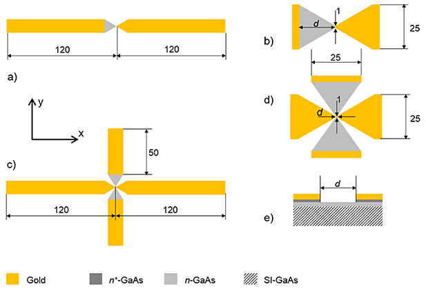
Figure 1. Schematic of investigated BT diodes (all dimensions are in μm): (a) asymmetric design, (b) enlarged active part of (a); (c) symmetric design; (d) enlarged active part of (c); (e) cross-sectional view of the active part along the x and z axes. xy coordinate system applies to (a)–(d).
Download figure:
Standard image High-resolution imageIn the asymmetric BT diode, the detected signal results from the nonuniform heating of carriers in the vicinity of the neck [23]. The asymmetry of contacts leads to a stronger electric field on the narrow side of the active area near the antenna tip. Because of the asymmetry in the carrier temperature, the diffusion of electrons from the hotter to the colder part of the channel results in the voltage signal across the sample. To ensure a sufficiently large difference in the carrier temperature, the distance between the antenna terminals d must significantly exceed the mean free path for electron energy relaxation. As discussed below and shown in figure 4(b), in GaAs, the electron energy relaxation distance is on the order of 1 μm. Therefore, the length of the active part must be at least several micrometers. In this study, it is assumed that the distance d is 10 μm for asymmetric BT diodes, similar to that used in the previously studied asymmetric devices [10, 13–16, 19, 23] in order to have rational references for comparison.
In the symmetric design, the thermodiffusion current is perpendicular to the current induced by the incident radiation. In this geometry, the symmetric tapered contacts along the x-axis act as bow-tie antenna leafs, while the other two contacts are used for readout of the detected voltage. The symmetric geometry allows one to reduce the distance between the antenna tips without the negative impact on the electron temperature gradient. The short distance between the antenna leaves is beneficial for increasing the heating electric field and decreasing the device impedance for better impedance matching between the device active area and antenna.
Simulations were performed to compare the efficiency of detectors of various designs. To calculate the detector responsivity to small signal THz excitation, we start with the simulation of relevant antenna parameters. The antenna impedance, directivity and efficiency are obtained using the commercial solver for RF electronics (the Advanced Design System software environment of Keysight Technologies). The metalized sectors of BT diodes are modeled as electrically thin planar antennas deposited on a semi-insulating GaAs plate. Then the antennas are represented as equivalent ac voltage sources. Following this approach here, we derive the impedance and the amplitude of the equivalent voltage source for a given incident power density. The voltage and impedance of the antenna electrodes are used as input parameters for further modeling the detector characteristics using the Synopsys Sentaurus TCAD. The equivalent ac voltage source is applied across the active part of the BT diode. Sentaurus TCAD solver was based on the classical hydrodynamic model consisting of the Poisson, electric charge continuity, current density and energy balance equations. The relevant GaAs material parameters were taken from the Sentaurus TCAD material database library. The calculated device sensitivity and impedance were used as parameters for comparison of BT diodes of the symmetric and asymmetric configuration.
BT diodes were simulated in two-dimensional geometry. In the asymmetric design, the active area was a trapezium with the base widths 1 μm and 25 μm (figure 1(b)). In the symmetric structure, the active area consists of two trapezoids connected through the central part of 1 μm × d μm (figure 1(d)). The active part is n-GaAs layer with donor concentration of 1016 cm−3. In simulated structures, the active part is terminated with 50 nm wide n+-GaAs layers with donor concentration of 1019 cm−3 for contacting the ac voltage source. The thickness of n+-GaAs layer is sufficiently larger than the thickness of the space charge region (≲10 nm) in n+-GaAs to provide non-rectifying contacts between the antenna metal and the active region. We assume that the heavily doped GaAs layers are in equilibrium with the metal contacts. Physical models involved in the solver were as follows: Fermi statistics; hydrodynamic transport for electrons and holes; doping dependent mobility; high-electric-field saturation of mobility including the electron transfer effect for hot electrons; doping dependent Shockley–Read–Hall recombination model; electron energy relaxation time of 1 ps [24]. In the simulations, the voltage was set to 0 V at one contact and the RF voltage source was connected to the other contact. All simulations were performed at 300 K with a time step equal to 0.01 of one oscillation period. Several oscillation periods (up to 15) were calculated until a stable solution was reached with deviations of the calculated values not exceeding 1 %. All relevant parameters of BT devices were extracted from the modeling of 1 μm thick device layer.
3. Results and discussion
The simulated antenna parameters are shown in figure 2. THz electric field is polarized along the horizontal antenna axis (x-axis). In the symmetric design, the impact of the signal readout contacts on the antenna characteristics were neglected for simplicity. As one can see, antennas of both types demonstrate almost identical parameters. Asymmetric design with one antenna leaf truncated has slightly higher resonant frequency and lower impedance.
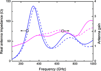
Figure 2. Real antenna impedance and antenna gain versus frequency of the BT antennas. Solid lines—symmetric configuration, dashed lines—asymmetric configuration.
Download figure:
Standard image High-resolution imageThe small signal impedance of the BT diode Zd was calculated using Sentaurus TCAD software at the resonant frequency of antenna. We found that for the asymmetric design Zd = (1584−j331) Ω at the frequency of 352 GHz and Zd = (500−j107) Ω at the frequency of 337 GHz for the symmetric design with d= 1 μm. Note that in the symmetric design, reducing the distance d leads to a decrease in the impedance of the device, therefore, better impedance matching between the detector and the antenna is achieved. The resonant frequency of the antenna was chosen in the frequency range above which the detector efficiency starts to decrease due to the finite momentum relaxation time, as can be seen from figure 7(b).
Further, we discuss the matching of the antenna impedance with the BT detector, which is important for optimizing the detector response. The active part is much smaller than the wavelength of the incoming radiation, therefore the BT detector can be characterized as a lumped element. In the case of perfect impedance matching the power absorbed by the detector is [25]:
where the antenna gain is given as G= ηD, η is the antenna efficiency, D is the antenna directivity, λ is the operating wavelength and I is the incident power density.
In the case of impedance mismatch the absorbed power P is smaller than Pmax. The mismatch factor [25]:
where the antenna impedance Za is obtained from the antenna S-parameter simulations [4], and Zd is the diode impedance.
In addition, the absorbed power is multiplied by 0.5 to account for the residual scattering of receiving antenna [26, 27]. The voltage amplitude of the effective voltage source on antenna terminals is [25, 28]:

By combining equations (1)–(3) we find that the voltage at the antenna terminals is 38 mV for the asymmetric design and 69.3 mV for the symmetric design (at d= 1 μm) when THz power density I is 0.1 mW mm−2 (it corresponds to a THz beam of power 0.058 mW focused to a spot with a diameter equal to one wavelength of an incident electromagnetic wave at the resonance frequency). The difference in antenna voltage between the studied structures depends mainly on the impedance mismatch factor given by equation (2) as the distance d has only a negligible effect on the antenna impedance.
To optimize the detector performance in the symmetric configuration device structures with the active part length d of 0.25 μm, 0.5 μm, 1 μm and 1.5 μm were simulated. The calculated complex impedance, the impedance mismatch factor and the antenna voltage are represented along with the detected voltage in table 1. The static resistance determines the detector noise power and the NEP value.
Table 1. Impedance of the active part of the BT detector, impedance mismatch factor, antenna voltage, detected voltage and static resistance for the symmetric design with d = 0.25 μm, 0.5 μm, 1 μm and 1.5 μm and for the asymmetric design with d = 10 μm.
| Symm., 0.25 μm | Symm., 0.5 μm | Symm., 1.0 μm | Symm., 1.5 μm | Asymm., 10 μm | |
|---|---|---|---|---|---|
| Impedance Zd, Ω | 124−j 24 | 283−j 76 | 500−j 107 | 647−j 155 | 1584−j 331 |
| Mismatch factor | 0.99 | 0.85 | 0.66 | 0.56 | 0.28 |
| Antenna voltage, mV | 73.8 | 69.3 | 60.4 | 55.9 | 38.0 |
| Detected voltage, mV | 0.88 | 0.79 | 0.34 | 0.24 | 0.016 |
| Static resistance, Ω | 1210 | 1062 | 910 | 818 | 1656 |
| Noise voltage, nV/√Hz | 4.48 | 4.19 | 3.88 | 3.68 | 5.24 |
In the symmetric BT diode, the tapered configuration of the BT antenna leads to the accumulation of induced charges at antenna tips and the concentration of the high-frequency electric field in a relatively small area between them. The electric field amplitude is plotted along the x-axis for samples with different lengths of the active part (figure 3(a)). The heavily doped regions are shown as shaded rectangles for reference. As expected, the electric field is confined mainly within the region with lower electron density. A decrease in the length d leads to a larger electric field amplitude. The incident electric field is 2.75 V cm−1 when the incident power density is 0.1 mW mm−2, as discussed previously. Note that the induced electric field remains nearly constant between the antenna tips, whereas it decreases along the y-axis (figure 3(b)) and vanishes at the side contacts. In fact, the side metal contacts act as antennas as well, however, their resonant frequency is far from the detector operating frequency, therefore, we neglect the electric field induced at the side contacts.
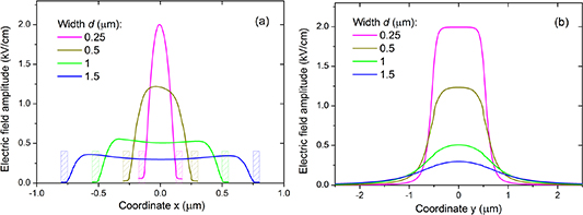
Figure 3. Electric field amplitude in the symmetric BT diode. (a) Along the antenna axis (at y = 0). (b) Along the direction perpendicular to the antenna axis (at x = 0). The coordinate reference point is set in the center of the active part. Shaded rectangles in (a) denote position of heavily doped areas.
Download figure:
Standard image High-resolution imageThe concentration of electric field results in a significant heating of free electrons in the central area of the active part. In figure 4(a), the electron temperature is shown between the antenna tips along the x-axis and in figure 4(b)—along the y-axis. The presented electron temperature is averaged over one oscillation period. Normally, the electron heating follows quadratic dependence of the electron temperature on the electric field amplitude. However, such behavior is found only in samples with wide antenna gaps—1.5 μm, 1 μm and 0.5 μm (compare figures 3(a) and 4(a)), whereas in the case of d= 0.25 μm the electron temperature is only slightly higher than that in the structure with d= 0.5 μm despite the remarkably larger electric field amplitude. This is a result of the energy loss of the hot electrons passing through the heavily doped contact regions. On the other hand, space limitations become of primary importance for electron energy to grow and reach steady-state value when the current path length decreases and approaches a certain critical length, which is in the order of hundreds of nanometers [29]. It is also seen that the hot electron energy relaxation distance extends to approximately 0.5 μm in the y direction relative to the corners of the antenna tips located at y = ±0.5 μm in agreement with theoretical estimation [6]. The temperature gradient along the y direction gives rise to the thermodiffusion current which is responsible for the detector response signal. Because of the device symmetry along the x-axis, the signal across the antenna leafs is negligible.
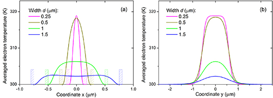
Figure 4. Averaged over period electron temperature in the symmetric BT diode. (a) Along the antenna axis (at y = 0); (b) along the y-axis (at x = 0). Shaded rectangles in (a) denote position of heavily doped areas.
Download figure:
Standard image High-resolution imageFor comparison, the electric field and electron temperature profiles were simulated for the conventional asymmetric BT diode (figure 5). As shown, the electric field is induced across the entire active part of the diode. In the asymmetric BT diode, the observed voltage signal appears due to the asymmetry of the temperature gradient caused by the asymmetry of the structure. Note that the electric field amplitude and electron temperature are remarkably lower in BT diodes with the asymmetric design. Therefore, the symmetric BT detector is expected to demonstrate larger thermoelectric voltage and higher sensitivity to the THz waves.
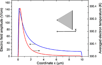
Figure 5. Electric field amplitude and averaged electron temperature in the asymmetric BT diode along the antenna axis. The reference point is set at the n-n+ interface at the narrow side of the active part. Inset—schematic of the active part, black areas denote heavily doped regions.
Download figure:
Standard image High-resolution imagePerformance of BT diodes of both types is presented in table 1 and figure 6. In the symmetric design, voltage is calculated between one of the antenna leafs and one of the side contacts and DC voltage component (detected voltage) is extracted. The symmetric BT diode also allows operation in the bolometric mode, in which DC current is passed vertically along the y direction (this mode is not discussed here). In the asymmetric design, the current along the x direction is calculated and DC current component is extracted. The detected voltage is obtained as a product of DC current and device static resistance. The responsivity is calculated as the ratio of the detected voltage to the incident THz power of 0.058 mW (see equations (1)–(3) and their comments). The NEP of the detectors is calculated as the ratio of the voltage noise and responsivity (figure 6). For unbiased operation, only the thermal noise is taken into account. The values of noise voltage are shown in table 1. In fact, the symmetric design of the BT diode consists of two equivalent detector structures. To calculate the NEP, we assume that the antenna leafs are DC-short connected via the antenna current nodes, and the side contacts have a short circuit for use as another detector terminal. In this scenario, two diode structures are connected in parallel, which leads to a decrease in static resistance and noise voltage.
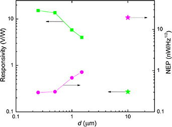
Figure 6. Responsivity (stars) and noise equivalent power (circles) of BT diodes against active area length. Solid symbols—symmetric design, open symbols—asymmetric design.
Download figure:
Standard image High-resolution imageIn figure 6, we show the responsivity and NEP of BT diodes of both types in the same graph versus length of the active part. It is seen that symmetric BT diode provides responsivity to THz radiation of up to 15 V W−1 and NEP as low as 300 pW Hz−1/2, more than one order of magnitude improvement over previously reported asymmetric BT devices. Note that the detector responsivity increases as the active area length is decreased. This is a combined effect of the reduced device impedance and increased concentration of RF electric field. Responsivity of the asymmetric BT diode is 0.3 V W−1, in agreement with the previously published experimental data [11]. Our calculations show that the responsivity of the symmetric BT detector increases with decreasing width of the antenna tips (in the direction of the y-axis), however, the device impedance also increases, which leads to lower absorbed power. To minimize the NEP, a tradeoff is needed between the responsivity, impedance and static resistance. Furthermore, larger hot-carrier thermoelectric signal occurs in materials with higher carrier mobility and at low temperatures, however, at the expense of reduced detection bandwidth [23]. Finally, implementation of the detector requires 3D electromagnetic simulation of BT diode integrated with the substrate lens according to specific application requirements. Modeling such optimizations is beyond the scope of this study.
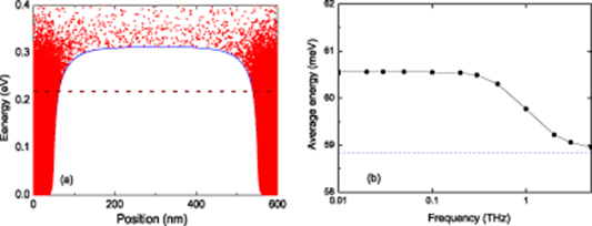
To verify the hydrodynamic modeling results of the symmetric design structure and to estimate the frequency limit of the detector, we performed the ensemble Monte Carlo (EMC) simulations using our simulation program. EMC calculations were performed for symmetric one-dimensional n+-n-n+ structure composed of an n-GaAs layer of 500 nm thickness sandwiched between two n+-GaAs layers of 50 nm thickness each. The n-GaAs doping was 1016 cm−3, and n+-GaAs was doped to 1019 cm−3. The amplitude of the applied ac voltage was 0.2 V. The nonparabolicity of Γ, L and X valleys and scattering of electrons by the polar optical, deformation acoustic, intervalley phonons, as well as ionized impurities were taken into account. The material parameters of n-GaAs are given in [30]. The electron-electron scattering and the Pauli exclusion principle were considered following [31]. The potential profile was found from the Poisson equation self-consistently coupled to the instant distribution of electrons and ionized impurities. The Poisson equation is solved at every time step using Dirichlet boundary conditions which are defined by the instant value of applied ac voltage. It was assumed that electrons are injected from the contacts with equilibrium Fermi–Dirac distribution [32]. Several periods of the applied voltage were simulated to attain the steady-state oscillations of the electron system.
The calculated potential profile and the electron energy distribution in n+-n-n+ structure are presented in figure 7(a). Figure 7(b) shows the hot electron energy in the middle n-GaAs layer averaged over one oscillation period. The presented EMC simulations indicate that the average electron energy is independent of frequency in the low-frequency range (to about 0.3 THz) and decreases with frequency in the high-frequency range in accordance with the Drude conductivity model. This factor limits the upper frequency of operation of the hot-electron detector. Accordingly, hydrodynamic calculations were performed under the same conditions for the one-dimensional n+-n-n+ structure. The average hot-electron energy was obtained at about 60 meV in the low-frequency range in agreement with EMC modeling. This fact justifies the choice of the energy flux factor of 0.28 used in the energy balance equation in hydrodynamic calculations.
Figure 7. (a) Potential profile (solid curve) and distribution of electron kinetic energy (points) at equilibrium; dashed line shows the Fermi energy; (b) average electron energy in n-GaAs layer against frequency of applied ac voltage; dashed line shows average energy at equilibrium.
Download figure:
Standard image High-resolution image
The NEP values of BT diodes are still inferior to those of commercial Schottky diodes [2, 33] and the state-of-the-art TeraFET detectors [28, 34], the production of bowtie diodes is much less demanding. In addition, the BT detector is characterized by high resistance to excessive input power as it does not contain easily vulnerable elements, such as a small-area isolated gate or rectifying metal-semiconductor contact. Finally, a DC short-circuit between the antenna leafs eliminates the DC potential difference in the gap, which provides additional internal protection against electrostatic discharge, which is always an issue in high-frequency electronic devices. At the next stage of research, it is planned to fabricate detector samples and optimize the parameters of symmetric BT detectors using both bulk semiconductors and two-dimensional semiconducting layers.
4. Conclusions
This article demonstrates a new design terahertz detector based on transverse hot-carrier transport in symmetric bow-tie diode. The geometry of the proposed device allows to reduce the spacing between the bow-tie antenna tips to submicrometer level, which leads to a significant enhancement of the heating electric field and improved impedance matching between the active device area and integrated bow-tie antenna. More than an order of magnitude increase in the device responsivity and a corresponding decrease in the NEP are shown in comparison with bow-tie detectors of asymmetric design. It was found that the optimal length of the active part is around 0.5 μm. Space constraints are of primary importance for electron energy to grow and reach a stationary value when the active part becomes shorter. The upper frequency limit of the n-GaAs BT diode reaches hundreds of GHz. These results demonstrate the new potential of BT diodes as fast and robust terahertz detectors in short-range communications, security and imaging systems.