

Abstract
In this work, technology computer-aided design (TCAD) simulation results of new CZT ring-drift detector geometries are presented. The physics model was developed and validated against the results from an existing device which had been comprehensively characterised at x-ray wavelengths. The model was then applied to new detector geometries and a systematic study of the parameters influencing charge collection performed. A comparison between one- two- and three-ring circle and semi-rectangular (or squircle) geometries is presented. In was found that charge collection with the squircle ring configuration was systematically better than the circular configuration and extends approximately  m further from the collecting anode. In addition, a two-ring geometry device is shown to collect charge
  m and
m and  m further from the anode when compared to one- and three- ring geometries, respectively. Based on these results, we derive an optimum configuration which potentially can be multiplied on larger crystals, offering an increased charge collection volume without compromising energy resolution.
Export citation and abstract BibTeX RIS

Original content from this work may be used under the terms of the Creative Commons Attribution 3.0 licence. Any further distribution of this work must maintain attribution to the author(s) and the title of the work, journal citation and DOI.
1. Introduction
Cadmium zinc telluride (usually denoted by  , CdZnTe or CZT) has emerged as the semiconductor material of choice for a number of x-ray spectroscopy applications in the nuclear industry [1], non-destructive testing [2], medical diagnostics [3] and space sciences [4] areas. It offers several advantages over silicon in the x- and
  -ray energy range between 20–500 keV. For example its density (5.8 g cm−3) is about twice that of Si and thus it has better stopping power, while its bulk resistivity (>
 cm) is much larger than Si allowing higher fields to be used for charge collection which in turn allow thicker devices to be fabricated. In addition, depending on the zinc fraction, its bandgap is typically 1.45–1.65 making it suitable for room or even elevated temperature operation. This negates the need for the complicated cryogenic cooling systems associated with the elemental semiconductors. However, a major disadvantage of CZT is wide disparity between the transport properties of electrons and holes. For example, there is an order of magnitude difference between its electron and hole mobilities, specifically 1350 cm2 V−1 s−1 for electrons and 120 cm2 V−1 s−1 for holes. Coupled with the fact that the mean free drift times are five times smaller for holes, the mu-tau (
 ) product of holes is thus 50 times worse than electrons. This means that the spectroscopic performance of a conventional planar detection system is limited by the poor
  product of the holes.
Single carrier sensing/correction is a technique that has been widely applied to CZT detectors to overcome poor hole transport. It achieves this by eliminating, or compensating for, the carrier with the poorest transport properties. Most approaches involve exploiting the near-field effect which can be induced by careful detector and/or electrode design. Particular implementations are: hemispherical and strip-drift geometries, coplanar grid and small pixel designs (for a review see [5]).
Technical progress in extending the collection volume and minimising the input noise in silicon drift detectors [6, 7] paved the way to apply the drift configuration approach to CZT detectors. In 1998, van Pamelen and Budtz-Jorgensen [8] applied the strip-drift method to CZT to reduce the electronic noise of the and correct for the residual effects of hole trapping. This was achieved by using an anode strip and drift strips on one side of the detector crystal in combination with a single planar electrode on the other side. Kuvvelti et al [9] demonstrated a marked improvement in energy resolution for a  mm strip CZT detector. They suggested that the strip-drift method can achieve energy resolutions which were within a factor of two of the Fano-limited resolution for CZT material. Gostilo et al [10] while further improving on energy resolution, concluded that for such configuration energy resolution at higher energies (661 keV) was limited by the transport characteristics of the charge carriers, even though the homogeneity of the selected crystals was high. The first CZT ring-drift detector, consisting of a point anode and control electrode, showed considerable improvement in energy resolution compared to the standard planar approach [11]. This approach was developed further through introduction of an analytical model and fabrication of the multi-ring drift configuration CZT detector in [12] and [13, 14]. This geometry was studied further in high detail by den Hartog et al [15] using a differential spectrometry analysis verified by fine x-ray scanning using highly tuned synchrotron beams. One of their key findings was unusual spatial response at lower energies, which suggested that the detector was insensitive over a large fraction of its physical area. This was considered to be an artefact of the current detector design, its ring geometry and biasing. Alruhaili et al [16] studied this geometry further and demonstrated independently that even though high energy resolution was achievable with such a topology, the charge collection volume was limited to a distance of 2 mm from the collecting anode on a
  mm device. Boothman et al [17] presented a comprehensive simulation study of the geometry characterised in [16]. The simulation model accurately recreated existing testing results and found optimised biasing conditions to improve charge collection extending to 2.5 mm. However, the problem of an ineffective charge collection volume has not fully been solved yet. On the
  mm crystal presented in [16] and [17], only the first 2–2.5 mm from the anode actually collect the charge, leaving the remaining 2.5–3 mm inactive. The present work capitalises on Boothman's simulation model and proposes a new geometry based on a
  mm CZT crystal. It lays the foundation for a higher efficiency detector unit cell which subsequently could be multiplied on
  and
and  mm crystals. This approach should lead to CZT detectors with a large active volume without a loss of energy resolution.
2. Materials and methods
2.1. Simulation package and model development implications
The Synopsys Sentaurus TCAD [18] finite element simulation package was employed to perform calculations in this study. The tools used were the Sentaurus Device Editor—a geometry structure editor, Sentaurus Device—a numerical simulation tool for electrical properties modelling, the INSPECT/Sentaurus Visual data visualisation programs and Sentaurus Workbench—a simulation flow management framework. Synopsys Sentaurus TCAD tools have several implications related to this study that were taken into account while conducting these simulations: the built-in models are mainly silicon specific and do not produce realistic results for compound semiconductors with default parameters; time related (or transient) simulations are limited to charge transfer from a single interaction only, meaning that a spectrum from a simulated detector cannot be built-up in a reasonable time frame; the charge generation mechanism is limited to alpha particles and heavy ions. Hence in order to simulate an x-ray interaction, additional steps are needed to realistically represent the charge cloud generated in the material.
2.2. Simulation model description
The realistic detector-grade properties of CZT used in this study were obtained from openly available data based on Redlen material [19]. Material from this manufacturer will be subsequently used to fabricate and characterise the detector based on the output and recommendations from this study.
2.2.1. Defects and resistivity.
The detector-grade CZT material resistivity exhibits values in the region of  cm. In order to achieve such resistivity values, a combination of defects were introduced in the form of acceptors and donors of a given energy, concentration and cross section, see table 1. Previous studies [20, 21] suggest that three shallow acceptor levels representing inherent material defects and one deep level responsible for the compensation mechanism are sufficient to adequately recreate realistic material resistivity.
Table 1. List of the defects introduced in the CZT model.
| Defect type | Energy (eV) | Concentration (cm−3) | Cross section (cm−2) |
|---|---|---|---|
| Acceptor |  + 0.023 + 0.023 |
 |
 |
| Acceptor |  + 0.290 + 0.290 |
 |
 |
| Acceptor |  + 0.480 + 0.480 |
 |
 |
| Donor | Ec - 0.830 |  |
 |
2.2.2. Mobility and life time.
The transport properties of the material are governed by the mobilities and life-times of the carriers. These were set such to achieve the  values for electrons and holes widely accepted in the literature for detector-grade material.
2.2.3. Injected charge definition.
X-ray interactions were simulated in the detector based on the heavy-ion model. Out of the two models available in the Synopsys Sentaurus TCAD, namely, alpha particle and heavy ion, the latter is known to be more adequate for the simulation of x-ray interactions. The parameters for the heavy-ion model were set to generate an electron-hole cloud expected for a 25 keV x-ray photon. The characteristic depth of the interaction was chosen such to achieve a 1/e attenuation length, corresponding to  m in CZT. This energy was chosen so the results of simulations validated against existing experimental data [16, 17, 22].
2.2.4. Charge collection definition.
Only a single photon interaction is allowed in the simulation package. The collected charge was calculated by integrating the electron current induced on the anode during the first 500 ns of the simulation time. The simulated values were benchmarked against the measurements. The same calculation method was later applied to compare between different geometries suggested for the new detector geometry.
2.2.5. Model validation.
The model was validated against the study of a manufactured device described in [16, 17, 22]. The device had dimensions of  mm (x-y -thickness). The charge collection was studied at the Diamond synchrotron facility using a monochromatic 25 keV
  mm beam across the centre of the detector. A 2D TCAD model of the geometrically equivalent device was created measuring
  mm. Because of the nature of the measurement, the 2D model was sufficient to qualitatively validate charge collection in the simulated device. Bias voltages applied to the model were replicated from the synchrotron measurements (R1 = −500 V, R2 = −600 V, R3 = −700 V, cathode = −700 V) with the exception of the guard ring, which was biased at −1000 V as the limitations of the TCAD would not permit correct boundary conditions at the edges of the detector model [22]. The validated model was applied to the new geometries to study the effects influencing charge collection and searching for an optimised geometrical arrangement.
2.2.6. Model biasing conditions.
Only one biasing scheme for this simulation study was chosen. The relative and absolute amplitudes of the voltages applied to the rings, cathode and guard ring were systematically studied in [17]. Their optimal voltages were chosen for this study, i.e. R1 = −1000 V, R2 = −1200 V, R3 = −1400 V, cathode = −1400 V, guard ring = −2000 V. Due to the length of each simulation, it was impractical to study further whether better biasing conditions exist for the new geometries. Such a study will be carried out on a fabricated device.
2.2.7. Simulated geometry models.
The detailed simulation performed by Boothman et al in [17] concluded that increasing number of steering rings from three to four to five does not improve charge collection. However, no conclusions on the designs with one and two rings were given. The devices created in this simulation study measure  mm. The collecting anode has a diameter of
  m. The thickness of the rings is
  m and the diameter of the starting point of the guard ring is
  m. Geometry models with one, two and three steering electrodes were simulated. In this study a comparison between a circle and squircle shape of the steering rings was performed. The geometry was developed such that only the diagonal cross section of the devices was different. This arrangement required a 3D model to be created for the comparison. A top view of the created geometries can be seen in figure 1. Charge collection was compared between the two sets of geometries. Charge was injected along diagonal X = Y axis at locations
  m, etc.
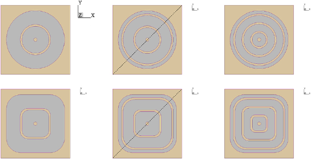
Figure 1. CZT detector configurations simulated in this study:  mm device; one, two and three rings; circle and squircle geometry of the rings. Charge was injected along diagonal X = Y axis, illustrated by a dashed line.
Download figure:
Standard image High-resolution image3. Results and discussion
3.1. CZT material properties validation
3.1.1. Resistivity.
The intrinsic material properties used in this study are based on three acceptors representing defects and one deep donor responsible for compensation. The initial trap energy levels, cross sections and concentrations were taken from [17, 22] and references therein. The macroscopic resistivity of the material can be directly calculated from the quasi-stationary simulation results with no bias applied to the detector by using formula
where q—unit charge, n and p —electron and hole concentrations,  and
and  electron and hole mobilities.
In the model created for this study resistivity was calculated to be  cm which falls within acceptable range for the detector grade material.
3.1.2. Charge carrier mobility and life-time.
The mobility and life time of the carriers were also extracted directly from the simulation results based on initial values set in the model configuration. They were found to be  and
and  cm2 V−1 for electrons and holes respectively.
3.2. Detector model validation
The micro-physics of the model was validated against a device fabricated and tested with a 25 keV  m micro-focus x-ray beam [16]. A simulation of the line scan across the centre of the detector was performed at a range of locations reported there. In the experiment, the centroid of the spectrum of the incident photons was plotted as a function of the beam position. In the Synopsys TCAD package only the charge from a single photon is allow to be simulated, hence a total charge induced on the anode was presented as a function of the interaction position for the model benchmarking.
Figure 2 illustrates the evolution of the current pulse as it was injected at different positions away from the anode. At the closest point to the anode position, the pulse is shown to have a symmetrical shape, denoting ideal charge collection through the detector bulk. Towards the furthest location, the current pulse not only degrades notably in height due to recombination, but also elongates due to trapping/de-trapping, since the charge takes longer to collect.

Figure 2. Evolution of the signal pulse injected at various positions along the detector and collected by the anode.
Download figure:
Standard image High-resolution imageFigure 3 shows a comparison between measurement and the model. The charge and peak position were normalised to unity at the interaction point under the anode for direct comparison. Inevitable discrepancies are observed in the charge collection between measurement and model. These are attributed to a variety of factors. Firstly, the measured doping concentrations of the defects in the real material have errors margins that are hard to precisely match in the model. Secondly, only a single 'representative' interaction is permitted at a specific depth in the TCAD simulations, which affects the spread of the interaction points as compared to the real measurement. Thirdly, the finite beam size adds to the ambiguity of the lateral interaction which cannot be adequately simulated with only a single interaction. The physics model along with any meshing, quasi-stationary and transient parameters were transferred directly into the 3D models to study new geometries for an optimised charge collection.
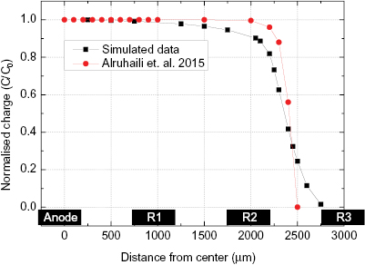
Figure 3. Line scan comparison between the results reported by Alruhaili et al in [16] and the present TCAD model.
Download figure:
Standard image High-resolution image3.3. Weighting potential simulations
The weighting potential visually illustrates how charge carriers drift inside a detector volume and produce a signal on the collecting electrode. The larger the value of the weighting potential, the larger the charge induced on the anode and hence the larger the signal. The same concept could be applied to the steering rings. Even though they do not collect the charge, the weighting potential from the rings shows the volume where the charge is influenced the most by a given steering ring. The simulations of the weighting potentials were performed for each geometry and each electrode. The given electrode was biased at +1 V while the other electrodes were kept at 0 V potential.
As expected, a comparison between the anode weighting potentials from all geometries indicate the 'small pixel effect' and an insensitivity of the anode to holes which are generated closer than  m from the anode where the weighting potential is larger than
  . This is illustrated in figure 4 for the three-ring squircle configuration. The weighting potentials from all the rings of the three-ring squirkle geometry are shown in figure 5 as a general illustration for all types of geometries simulated. Each geometry has subtle differences that influence charge collection. In order to further illustrate this, electron cloud snapshots were taken at different points in time during simulations. For illustrative purposes, charge was injected at 1.5 mm depth, 1.0 mm (x = y ). The transient simulations were conducted for 500 ns. The snapshots were taken for geometries with one, two and three rings squircle configuration. Figure 6 shows electron current densities at 40 ns (before any sizeable charge is detected at the anode), 120 ns (when the charge is peaked at the anode) and 300 ns (towards the end of the simulation). At 40 ns for the one ring configuration charge is visibly pushed down by the electric field of the ring preventing its drift towards the anode. Comparison between the two and three ring geometries at 40 ns show that the electric field is more effective in the two ring configuration as the charge is collected on the anode earlier. At 120 ns in the one and three ring configurations, charge is pushed towards the cathode, which is not observed in the two ring geometry. At 300 ns in the three ring case, the charge current density is higher at the origin of the charge, compared to the one and two ring configurations indicating that it would take longer to collect.
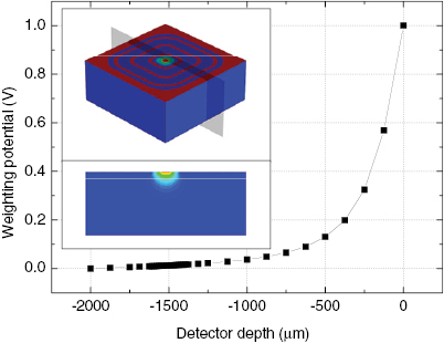
Figure 4. The weighting potential of the anode for the three-ring squircle geometry.
Download figure:
Standard image High-resolution image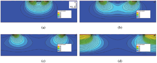
Figure 5. Weighting potential of the three-ring squirkle configuration. (a) Ring one. (b) Ring two. (c) Ring three. (d) Guard ring. Vertical (Z) scale is  m, horizontal (diagonal X = Y axis) scale is
  m.
m.
Download figure:
Standard image High-resolution image
Figure 6. Electron current densities simulated for one, two and three ring squircle configurations. Snapshots are taken at 40, 120 and 300 ns. Vertical (Z) scale is  m, horizontal (diagonal X = Y axis) scale is
  m.
m.
Download figure:
Standard image High-resolution image3.4. Evaluation of geometry options
A comparison between different geometries was performed in a similar way to the synchrotron studies on the benchmarked device. Since at the centre of the device along x and y axis' alone, circle and squircle geometries are identical, the charge was injected at various positions along diagonal x = y axis. It is assumed that the response along either x or y axis for both circle and squircle ring arrangements would be the same.
3.4.1. Shape of rings study.
Figure 7 shows a comparison between the three ring squirkle and three ring circle configurations. The charge collection remains similar between the two configurations until approximately  m. After this, the three ring squirkle configuration shows improved charge collection. In this geometry, the device remains sensitive to charge injection until approximately
  m, while the three ring circle configurations stops collecting charge after about
  m. Figure 8 shows a comparison between the two ring squirkle and two ring circle geometries. The charge collection in this case remains similar between the two configurations until approximately
  m. After this the two ring squirkle configuration shows improved charge collection by being sensitive to charge injection until
  m, whilst the two ring circle configurations stops collecting charge after about
  m. A dip in the charge collection in the two ring squirkle can be noticed between
  m and
m and  m. This feature is observed right below the first ring. Because such a dip is only observed prominently for the two ring squirkle geometry, it seems that the biasing conditions for this ring could be further improved to optimise charge collection in this region of the device. Figure 9 compares the one ring squirkle and one ring circle geometries. As for the three and two ring configurations, the squirkle geometry improves charge collection. The one ring circle geometry collects charge until about
  m, while the device with one ring squirkle configuration collects charge until ∼
 m. It is worth noting a small dip around
  m for the one ring circle geometry. Because it is located between the anode and first ring, it can be attributed to the weakest point in the weighting potential. This can be improved by careful optimisation of the biasing of the first ring.

Figure 7. Charge collection comparison between three ring squirkle and three ring circle configurations (along diagonal X = Y axis).
Download figure:
Standard image High-resolution image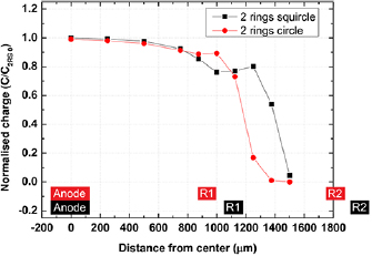
Figure 8. Charge collection comparison between two ring squirkle and two ring circle configurations (along diagonal X = Y axis).
Download figure:
Standard image High-resolution image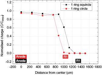
Figure 9. Charge collection comparison between one ring squirkle and one ring circle configurations (along diagonal X = Y axis).
Download figure:
Standard image High-resolution image3.4.2. Number of rings comparison.
The squircle steering ring configuration has been shown to be systematically better than the circle ring configuration. A comparison between the number of the rings in this geometry is shown in figure 10. Charge collection extends as far as ∼ m from the anode in the two ring configuration case. This gets worse for both the 3 and 1 ring geometries. The one ring configuration collects charge until
 m while the three ring geometry device—until ∼
 m. It is worth noting the pulse timing attributes of the geometries simulated. Figure 11 depicts three selected charge pulses from the one, two and three ring squircle geometries. Charge was injected at a distance of
  m from the anode. The total charge collected is marginally different between the two and three ring and
  smaller for the one ring geometries at this location. However, the times the pulses start to be collected by the anode differ. The first charge starts being seen on the anode is 50 − , 75 − and 85 ns for two, three and one ring configurations respectively. This indirectly confirms the more effective weighting profile for the two ring geometry. When charge is collected faster by the anode, there is less probability for recombination, which is likely to be pronounced more in a real device.

Figure 10. Charge collection comparison between one, two and three rings squirkle configurations (along diagonal X = Y axis).
Download figure:
Standard image High-resolution image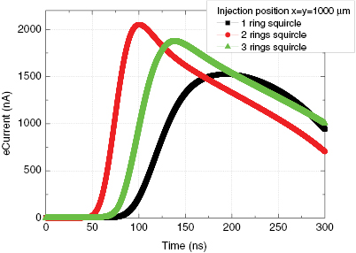
Figure 11. Pulse shape comparison between one, two and three rings squirkle configurations. Charge was injected at position  m.
m.
Download figure:
Standard image High-resolution image3.4.3. Device thickness and increased bias comparison.
The study of the two ring squircle configuration was extended further. A comparison was made for the device with double the thickness (4000 instead of  m) and double the default bias, R1 = −2000 V, R2 = −2400 V, R3 = −2800 V, cathode = −2800 V, guard ring = −4000 V. It was expected to see a change in the weighting potentials of the rings and hence variation in the charge collection.
Figure 12 shows the extension of the charge collection range for the  m thick device. In this case, the charge is being collected all the way to the start of the second ring (approx.
  m). This is improved by
  m compared to the nominal thinner device. The increase of charge collection when applying a factor of two increase in bias voltage is shown to be marginal, yielding only a ∼
 m extra.
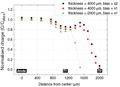
Figure 12. Charge collection comparison for the two rings squirkle configuration with twice the device thickness and bias.
Download figure:
Standard image High-resolution image4. Conclusions
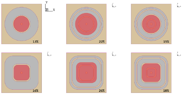
In this study a model based on Redlen CZT material was created. The basic properties were simulated and appear to be consistent with detector grade material. A detector model was created to follow the geometry properties of a device whaich dad been comprehensively studied with a collimated monochromatic 25 keV micro-beam x-ray source. Taking into account the limitations of the Synopsys TCAD, a realistic response was confirmed by performing simulations that mimic an x-ray scan across the detector surface. The model was then transferred to new geometries based on a  mm die in order to find one with the largest charge collection volume. In total, six geometries were compared in this study. Circle and squircle configurations with one, two and three rings were assessed. The squircle configuration was found to be systematically better for each of the three rings devices. The charge volume was extended by approximately an extra
  m with the squircle geometry. Out of the three ring configurations, the two ring geometry showed the largest extent of the collection volume being sensitive to charge up to
  m as compared to
  m for the one ring device. Figure 13 visualises charge collection regions. The fraction of total device area is shown for each geometry. For comparison, Boothman et al achieved maximum of
  collection area in their work [17, 22].
Figure 13. In red is the charge collection region as seen from the top of the device. Numbers in the corners are charge collection as fraction of the total device area.
Download figure:
Standard image High-resolution image
The simulation was extended to a 4 mm thick device with double the bias voltage for the two ring squircle configuration. The charge collection region was found to be extended even further by  m for the same interaction depth. This simulation work does not include optimisation of the biasing conditions of the proposed geometries. Such a study will be performed on a fabricated device. As indicated by Boothman in [17] and being observed during this study, the device biasing conditions can be improved further to optimise charge collection volume for different x-ray energies. The optimised geometry concluding this study is applicable to a
  mm CZT die. The dimensions of the anode and rings were designed such that the two ring squircle geometry can be multiplied on
  mm and eventually
  mm dies to increase charge collection volume with little compromise of energy resolution.
Acknowledgments
This work has been supported by the STFC grant ST/N000358/1.