

Abstract
Phase-change materials (PCMs) that can reversibly transit between crystalline and amorphous phases have been widely used for data-storage and other functional devices. As PCMs scale down to nanoscale, the properties and transition procedures can vary, bringing both challenges and opportunities in scalability. This article describes the physical structures, properties and applications of nanoscale phase-change materials and devices. The limitations and performance of scaling properties in phase-change materials and the recent progress and challenges in phase-change devices are presented. At the end, some emerging applications related to phase-change materials are also introduced.
Export citation and abstract BibTeX RIS
1. Introduction
Data storage media have always been important for human civilization, from cave paintings, printing, and photographs to magnetic tape. In recent years, the advent of solid-state data storage device has sped up the pace, making information easier to store in many regards. Among various emerging storage technologies, phase-change materials (PCMs) are widely considered a promising candidate for next-generation solid-state data storage devices [1, 2]. PCMs have been extensively used in re-writeable Blu-Ray discs and numerous new applications. They can reversibly transit between crystalline and amorphous phases and be repeatedly switched between these two phases through local crystallization, melting and rapid cooling, as shown in figure 1. Thus, the phase stability and transitions of PCMs are at the heart of phase-change memory devices. Information can be then encoded in these two phases as 1 or 0 bits, which show a distinctive contrast in electrical and optical properties. This extraordinary effect was first discovered in 1968 [3]. However, it took approximately 20 years to make a real breakthrough, when pseudo-binary GeTe and Sb2Te3 materials started to be used for optical data storage [4].
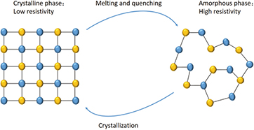
Figure 1. Schematic graph of phase change processes between amorphous phase and crystalline phase.
Download figure:
Standard image High-resolution imageIn recent years, scientists and engineers have refocused on the electronic memory applications of phase-change memory, utilizing electrical conductivity rather than reflectivity [5, 6]. Here, phase-change memory is achieved by the large electrical resistance contrast between the amorphous and crystalline phases in PCMs [7], in which the resistance of amorphous states can be three or four orders of magnitude higher than that of crystalline states. A long current pulse (set current) can be applied to heat the amorphous material above its crystallization temperature to induce recrystallization, whereas a higher short current pulse (reset current) can heat the crystalline phase and melt the material, enabling rapid cooling (melt-quenching) to form the amorphous states, as shown in figure 2(a). For electrical switching memory, one important phenomenon is the so-called threshold switching effect: when the phase-change memory is in the amorphous state or so-called reset state, a rather moderate threshold voltage can lead to a drastic reduction in resistance, producing enough heat to recrystallize the memory, as shown in figure 2(b). These effects discussed above are crucial for the functionality and performance of phase-change devices and are related to the properties of PCMs.
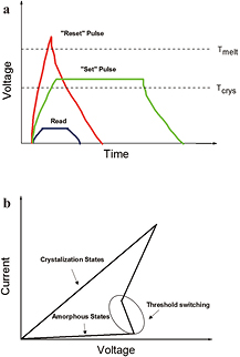
Figure 2. Principle of electrical phase change memory. (a) The programing of a electrical phase change device: a high voltage is applied to a volume of crystalline phase change materials, leading to melting and then rapidly quenching (reset pulse); a lower power pulse which hold the amorphous phase change materials for sufficient time for recrystallization(set pulse); a low voltage is used to sense the device resistance (read). (b) Current–voltage curve of a typical threshold switching process.
Download figure:
Standard image High-resolution imageA major concern in the development of PCMs based applications is their scalability. On the single-device scale, diminishing dimensions are favorable for lowering power consumption. From the system perspective, device scalability results in higher storage-data density and cost reduction. The scaling properties of both PCMs and devices need to be discussed. The properties of nanoscale PCMs can be different from those of bulk materials, leading to distinct phase transformation energetics and structural stabilities. Scaling the devices also brings opportunities and challenges for large-scale device fabrication. In this article, we focus on recent developments in nanoscale PCMs and devices. For more information on the atomic structure, chemical transformations, and applications of PCMs and memory, we refer to other excellent reviews [1, 2, 6, 8–14]. We discuss the properties and crucial parameters of PCMs as they shrink down to the nanometer scale. Then, we focus on nanoscale phase-change devices and present some excellent designs for ongoing improvements in device performance aspects such as lower power switching, high endurance, data retention time and multi-level cell applications. Furthermore, we present other potential applications that take advantage of the unique abilities of nanoscale PCMs. Notably, PCMs can be applied to other fields such as topologic, optic-circuit, thermoelectric and neuromorphic applications.
2. Properties of nanoscale PCMs
In the last two decades, the scaling properties of PCMs have been intensively investigated. Nanoscale phase-change thin films [15, 16], nanowires [17–21], and nanodots [22–24] have been synthesized and characterized, as shown in figure 3. Phase-change thin films can be conveniently fabricated by deposition processes [8]. Phase-change nanowires have attracted scientific and engineering interest due to their single-crystalline structures and tunable sizes [10]. Phase-change nanoparticles offer another platform to study the size limit of phase changes [25]. To produce nanostructure materials, several fabrication methods, such as sputtering deposition [8, 15], e-beam lithography [26], and chemical vapor deposition [27], can aid in the accurate control of the material scale [8]. Nanoscale defect engineering [28], dislocation engineering [29] and interfacial engineering [30] have also been widely used in the development of PCMs. Their electrical [31–33] and thermal [34] properties have been demonstrated at the atomic level to explore the scaling limits of PCMs.
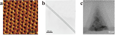
Figure 3. Transmission electron microscope of different kinds of phase change materials. (a) thin film with nanoscale bits patterns (b) nanowire (c) nanodot. (a) Reproduced by permission from Macmillan Publishers Ltd: Nature Materials [16], Copyright (2006). (b) Reprinted with permission from [20]. Copyright 2007, American Chemical Society. (c) Reprinted from [24], with the permission of AIP Publishing.
Download figure:
Standard image High-resolution imageThe performance of a nanoscale PCM device, including the set and reset power, on/off ratio, speed, and reliability, is strongly dependent on the electrical and thermal properties of the nanoscale PCM. In the following sections, we focus on the parameters of PCMs that are crucial for device applications, which are summarized in table 1. We review each parameter, including the crystallization temperature, melting temperature, thermal conductivity, threshold voltage, crystallization speed, and resistance contrast, to discuss the scaling law of these parameters.
Table 1. Materials properties that are related to the performance of PCM.
| Materials properties | PCM device performance |
|---|---|
| Crystallization temperature | Data retention time, set power |
| Melting temperature | Reset power |
| Resistivity | On/off ratio |
| Threshold voltage | Set voltage, reading voltage |
| Thermal conductivity | Set and reset power |
| Crystallization speed | Set pulse duration, data retention |
2.1. Crystallization temperature Tx
The crystallization temperature (Tx), the lowest temperature at which the crystallization process occurs, is a particularly important parameter. Tx sets a definitive and easily measured bound on the retention versus temperature curve for PCMs, which can be measured by raising the temperature slowly while monitoring the crystallinity [2]. Typically, a high crystallization temperature leads to better thermal stability and longer data retention time [13]. Multiple methods, including doping [35] and various material systems [36, 37], have been attempted to improve the crystalline properties.
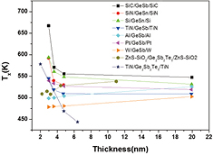
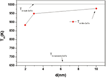
Interestingly, correlations have been reported between Tx and the dimension of the PCM. Generally, the Tx of PCMs sandwiched between oxides or nitrides can increase exponentially as the thin film thickness decreases [15, 24, 38], which can be explained by the inhibition of crystallization for very thin adjacent interfacial layers in semiconductor materials [39]. However, different interface materials can strongly influence the Tx in thin films. For instance, metal-induced crystallization can occur in PCMs sandwiched between metals. As a consequence, the crystallization temperature can reduce significantly, reaching 200 °C [30]. The influences on Tx of different interfacial layers are summarized in figure 4. Distinct interface capping materials introduce compressive stress to PCMs, thus strongly modulating Tx [38].
Download figure:
Standard image High-resolution imageCrystalline-crystalline phase transition temperatures have been reported to show film thickness-dependent properties in different material systems due to the interfacial free energy, which provides important insight into the multi-level applications of phase-change phenomena [36, 40, 41].
For nanowire devices, the phonon-softening model has predicted that as the diameter of the nanowire decreases, the enhanced phonon softening with an exposed broken band on the heterogeneous surface will suppress the Tx [28]. Measurement on Ge2Sb2Te5 showed that smaller diameter nanowires have lower activation energies, indicating a shorter data retention time [42]. However, Yu et al [43] did not observe a dependence of Tx on the nanowire diameter. For phase-change nanodots, a different trend is observed than that in the thin film, which is explained by the heterogeneous nucleation [44]. In exploring the ultimate size, nanoparticles as small as 2 nm have shown amorphous-crystalline transitions, indicating good scaling properties [45]. Nanocrystalline technology has also been applied to increase the Tx by the internal stress effect [46, 47]. The scaling properties of the crystalline temperature of PCMs shows promising potential for next-generation phase-change technology, and effort is needed to develop unique material systems for specific application requirements [28].
2.2. Melting temperature Tm
High reset energy has been a bottleneck in the development of phase-change memory. A low PCM melting temperature (Tm) is generally beneficial to the device performance because it indicates a reduction in the power required to reset a phase-change memory device. Fortunately, Tm can vary with composition [48] and dimension. With reduced dimensions, thin films [7], nanowires [20] and nanoparticles [49], have been reported with significantly reduced Tm values (figure 5), mainly due to the increasing ratio of surface atoms to volume atoms.
Download figure:
Standard image High-resolution imagePCMs have also been mixed with different substances that have higher melting temperatures. For example, nitrogen doping Ge2Sb2Te5 leads nitrogen to preferentially bond to Ge atoms [48]. Wang et al [44] found that this microscopic phenomenon helps maintain the grain size structure of Ge2Sb2Te5 because the melting temperature of nitrides is higher than that of Ge2Sb2Te5, increasing the overall endurance of the device. Pressure also plays an important role in Tm. Theoretical and experimental investigations have shown that amorphization and crystallization can be achieved under elevated pressure [50, 51], and the internal pressure can be high due to the volume change during phase transition [52]. The melting temperature can increase, leading to an increased 'reset' operation energy [53]. Overall, diminishing dimensions result in the reduction of Tm, which is favorable for decreasing the power of the reset step. Many other microscopic structure effects, such as interfaces and doping, can play important roles in determining the Tm, indicating that the design of PCM systems on the micro- and nanoscale should be deliberate and comprehensive.
2.3. Thermal conductivity
PCM devices require temperature-driven phase transitions. Thus, thermal properties play a central role in this technology [34, 54]. Researchers have extended nanoscale heat transfer measurement methods, such as TDTR [55] and 3ω [56], to reveal exciting thermal transport phenomena of PCMs. Thermal transport in PCMs are intriguing because several material phases can coexist depending on the temperature history, geometry, neighboring materials and process details [34, 57, 58]. Moreover, anisotropic thermal conductivity can be an important parameter in the crystalline phase due to the remaining nanoscale amorphous phase near grain boundaries [55]. Phase-change nanowires have also been reported to show rather small thermal conductivities in the amorphous and crystalline phases [59].
In addition, electron and phonon heat transport properties play influential roles in the thermal properties of PCMs. For instance, although atomic vibrations are mainly responsible for heat conduction in the amorphous phase, electron heat transport can become prominent in the crystalline phases of Ge2Sb2Te5 [21, 34, 60]. The difference in heat conductivity in different crystalline phases is well explained by separate electrical measurements and the Wiedemann–Franz law [49, 50].
Thermal boundary resistance (TBR) is another crucial parameter for the performance of nanoscale PCMs, because as dimensions diminish, most excess energy is required to reset the device flow through the interface between the electrode and the PCM [61] and through surrounding materials [50, 62]. The TBR between dielectrics [63, 64], metals [62, 65] and carbon-based materials [51] has been investigated, in which the distinct TBR between different phases of PCMs can be attributed to different acoustic and lattice structures, which can be explained by the phonon diffuse mismatch model [65]. Furthermore, study of the interplay between electrons and phonons through the interface suggests that, in all phases of Ge2Sb2Te5, phonons govern the boundary thermal transport rather than electrons due to the small amount of electron tunneling transport [60]. To localize heat, the dielectric staking method has also been used to minimize the surrounding thermal conductivity [50, 60]. The study of TBR is beneficial for understanding and improving the thermal isolation of PCMs.
2.4. Threshold voltage
The threshold voltage is a parameter of PCMs that describes the applied voltage required to induce an electrical breakdown effect, which has been assumed to be related to the structural instability under a high electrical field [66, 67]. This sudden increase in electrical conductivity enables PCM devices to rapidly and efficiently attain sufficient energy to recrystallize at a moderate voltage. Hence, materials that show threshold switching are essential for phase-change device applications [66–68].
Studies of phase-change devices have shown that the threshold voltage scales linearly with the length from the bridge along the applied voltage direction [5, 69], suggesting a material-dependent threshold field rather than a threshold voltage that should be surpassed for the amorphous material to become conductive, as shown in figure 6(a). However, according to the impact ionization model [70], the scaling law fails when the length is less than 10 nm [43], which is very favorable for scalability because the read current in the circuit may be higher than the reset current through the nanoscale phase-change device. Stochastic network and electrical-temperature fields are applied to explain the scalability of the threshold phenomena at the microscopic level [71, 72]. It has been reported that a sub-threshold electrical field could be applied to accelerate structural modification to modulate the threshold voltage, which is beneficial for control and improvement of the phase-change device performance [29, 73–75]. In addition, contact resistance is an important parameter for threshold voltage in nanoscale devices. With reduced dimensionality, contact resistance plays a more important role in the overall electrical resistance, thus greatly influencing the threshold voltage [76, 77]. Additional detailed information on contact resistance is given in section 3.2.
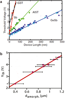
Figure 6. The scaling properties of threshold voltage of phase change materials. (a) Threshold voltage versus device length. Linear fits are used to determine the threshold field. Different symbols indicates different bridge width. (b) Threshold voltage as a function of the size of the amorphous region. (a) Reprinted from [69], with the permission of AIP Publishing. (b) Reprinted with permission from [46]. Copyright 2011, American Chemical Society.
Download figure:
Standard image High-resolution imageTo explore microscopic aspects during threshold switching, advanced experimental methods, including in situ TEM, have been applied to observe the phase change process. Meister et al [19] observed void formation during threshold transitions, and theoretical calculations have been conducted to show that electrical field effects may play a significant role in threshold transitions [71]. Furthermore, the relation between the nanostructure-amorphous phase change inside devices and threshold switching has been investigated, indicating a linear relationship between the threshold voltage and the scale of the amorphous domain [46], as shown in figure 6(b). This result can explain the observed variability in PCM switching measurements.
2.5. Crystallization speed
Speed is likely critically important for PCM devices because it sets an upper bound on the potential data rate [2]. Three processes determine the operation speed: read, reset and set. Generally, the set process (amorphous to crystalline transition) takes the longest of these three processes due to the slower kinetics of forming crystalline (lower resistance) state than of forming an amorphous (higher resistance) state [6]. Thus, improving the crystallization speed is central to accelerating the overall speed.
The formation of the crystalline phase involves four steps: (1) threshold switching [66], (2) current-induced heating to an elevated temperature, (3) crystal nucleation [33] and (4) crystal growth. The nucleation step can be slow in so-called growth-dominated materials, whereas nucleation-dominated materials generally have a lower barrier to nucleation [6]. PCMs can be divided into these two groups, depending on the nucleation and growth kinetics; various researchers have been working to reveal and supplement understanding of the microscopic and macroscopic structures of this process [6, 78, 79].
Several factors contribute to the nucleation and growth kinetics in PCMs [6]. Among them, scaling has a strong influence on the crystallization speed. It was reported that the crystallization speed of amorphous Ge2Sb2Te5 can decrease significantly when the device dimensions decrease due to interfacial effects [80, 81]. A superlattice has been introduced to build an interfacial phase-change memory with faster transit speed [82]. In addition, nanostructure engineering technology has been used to investigate and improve the crystallization speed of phase-change devices. In GeTe-based devices, a similar decrease in set speed is observed, and it was argued that the size of the amorphous region may play a critical role in the diminished growth-dominated recrystallization process time [83]. Loke et al [74] showed that applying a weak electrical field can greatly accelerate the recrystallization process to 500 ps due to nanostructure pre-ordering, as shown in figure 7. In addition, crystallization mechanisms different than those of bulk materials, such as hetero-crystallization mechanisms [44] or autocatalytic phase-change processes [84], may play important roles when devices are downscaled and may overcome the limitations between speed and reliable quality [44]. Finally, in contrast to the crystallization model, a purely electronic model for threshold switching has been applied to describe the phenomenon of ultrafast crystallization of Ag4In3Sb67Te26, indicating the potential for an ultrafast electronic switch [44]. The device history [26, 81], multi-phase (multi-level) technics [85, 86], temperature [79, 86, 87], and diverse material systems [88, 89] also strongly influence the crystallization speed.
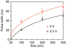
Figure 7. Size dependent switching speed. The pulse width decreases with the incubration voltage, further improving the speed. From [74]. Reprinted with permission from AAAS.
Download figure:
Standard image High-resolution image2.6. Resistivity ratio and conclusions for PCMs
The ratio between the resistivity in the amorphous and crystalline phases directly determines the on/off ratio of PCM devices and has a strong influence on the amplitude of the set and reset current [2]. Though theoretical studies predict that the resistivity ratio will decrease when the dimensions decrease below a dozen atomic layers [90], nanoscale PCMs do not generally show this phenomenon [78]. However, to meet the demanding requirements of data storage, multi-phase technics may be required to increase the device density. Thus, it would be necessary to manipulate the resistivity ratio to enable multi-phase change switching. Details of the multiphase-switching device are discussed in section 3.3.
PCMs generally demonstrate highly desirable scaling behavior, which can be extended over several generations of technology nodes [11]. Further efforts of scientists and engineers will reveal the microscopic mechanisms of different phase-transition processes and new materials systems to achieve an overall balance and improve the performance of devices through nanostructure-engineering and scaling to precisely manipulate the phase-change properties.
3. Challenges of nanoscale phase-change memory applications
Renewed interest in PCM technology was triggered by the discovery of fast crystallization materials [91, 92]. Since then, there have been many integration efforts in advanced PCM technology [2]. High-endurance [93], rapid [94] devices have been made to meet various standards of practical applications. In the last five years, PCM density improvement (device-to-device pitch scaling) and aggressive scaling of PCM devices have led to a reduction in the required reset power, which is an underlying strength of PCM devices [13]. The largest arrays have billions of bits per memory chip, bringing technologies within the range of the density of incumbent memory technologies [13]. Here, we briefly introduce some PCM applications and important challenges.
The first application is in stand-alone data storage to compete with flash memory [95]. It requires only moderate operation temperature, cycle numbers and switching speed (ns range), and Ge2Sb2Te5-based alloys can provide the required material properties and switch much faster (ps range). For high-speed hard drives [96], the cycle number is a high standard, and doped Ge2Sb2Te5 material systems may be necessary to reach the criterion. For automotive applications or pre-coded chips, high-temperature endurance is required, so additional doping of Ge-Sb-Te materials or GaSb is suitable for these applications [97–99]. Dynamic random access memory (DRAM) is a formidable challenge, requiring both rapidity and high cycle number (endurance). Rapid speeds have been achieved in several material systems [29, 74], but higher cycle numbers are difficult to reach. However, scaling properties may help increase the cycle number by complete melting to avoid element segregation [7].
An important obstacle in the scaling of PCMs is the access device, which should be larger than the PCM cell to provide sufficient current, thus limiting the storage density. Here, lowering the reset power of phase-change devices is an efficient method to reduce the size of the access device and consequently increase the storage density. Another important solution is to apply multi-phase technology, which can directly increase the data density. Moreover, the device reliability, including the retention, endurance and polarity effect also strongly influence the lifespan of nanoscale phase-change devices. In the following section, we focus on the challenges and opportunities of the reset power, the reliability of nanoscale phase-change devices and multiphase applications, as well as the solutions that scientists and engineers have developed to meet these challenges.
3.1. New designs to overcome high reset power
Reset power is closely related to the reset process, in which the crystalline phase of a PCM transitions to the amorphous phase. It was assumed that this transition requires heating the material above its melting temperature, which determines the general power consumption of nanoscale phase-change devices. In general, scaling can greatly decrease the reset power [15, 17, 42]. However, sufficient reset power is still necessary to minimize the feature size of PCMs and increase the data density. As noted in the previous section, the access device current is a major challenge in this aspect, and thus one method for improving the data density of nanoscale phase-change devices is to improve the general capability of the access device [2]. Another solution is to locally increase the current density in the PCM and decrease the switching volume, as presented below.
The industry has proposed brilliant designs using sub-lithographic aperture and doping methods [100, 101]. Among them, contact-minimized cells and volume-minimized cells are two general categories, as shown in figure 8(a) [2]. A contact-minimized cell minimizes the switching energy by introducing a mushroom-like nanoscale amorphous dome of PCM, resulting in an overall high-resistance state. A volume-minimized cell minimizes the volume of the PCM, thus lowering the reset power by scaling. Theoretical calculations suggest that these geometric properties may strongly influence the cell power efficiency [102].
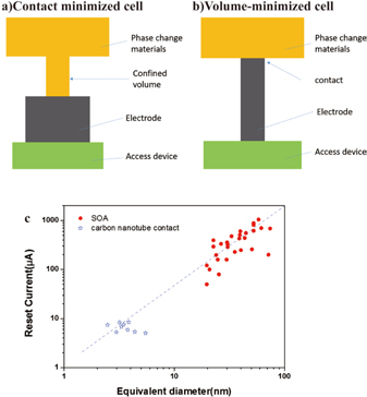
Figure 8. The scaling properties of reset power of phase change devices: A schematic graph of (a) a typical contact minimized cell and (b) a typical volume-minimized cell. (c) Scaling of reset current reported by Xiong [103] and Wong et al [1].
Download figure:
Standard image High-resolution imageRecent effort to lower the reset power has focused on improving the thermal efficiency using these two methods by balancing the cell resistance against the programming current [13]. Here, the contact electrode can greatly influence the power consumption [76]. Thus, carbon-based materials, such as carbon nanotubes or graphene ribbons, have been used as electrodes to decrease the overall energy consumption due to their sharp, atomically thin edges. Feng et al [103] presented a significant reduction in power using carbon nanotubes and found scalability between the electrode area and reset power, as shown in figure 8(c). Graphene was added at the interface [104] and electrode [77] between the PCM to aid in efficient Joule heating. Additionally, a superlattice PCM stack has been shown to lower the thermal conductivity [105] and change the switch mechanism to short-range movement instead of order-disorder transitions [106]. This ability has led to reduced power consumption and improved endurance [82]. The performance and power are improved by optimizing the stack design and decreasing the cell size [107, 108]. In addition, small cross-sectional and nanostructure-engineering devices, including phase-change nanotubes, have also been used to lower the switching power [28].
3.2. Reliability
Endurance is one aspect of reliability. Though PCMs generally enable good endurance properties (over 108 cycles), cycling-induced degradation generates early tail-bits that trigger read errors [13]. There are three typical tail-bit behaviors: cell open, stuck-high and stuck-low. These failure mechanisms are related to void formation and phase segregation [19, 109, 110]. Void formation is due to repeated changes in volume during switching by mechanical stress, and phase separation is driven by incomplete melting and recrystallization at the liquid-solid boundary [111, 112]. Thus, complete melting can aid in solving the problem of phase segregation [13]. Another method to avoid phase segregation includes manipulating the electrical pulse to reduce electromigration [113] or rejuvenating stressed PCM cells [114].
Another important aspect of reliability is material retention. To be applicable as a real candidate for nonvolatile memory, the PCM must demonstrate the long-term retention of stored data. The stability of the quenched reset phase dominates the retention issue because the crystalline set state is generally stable at room temperature. Here, thermally activated crystallization of the amorphous phase leads to a reduction in the resistance and causes retention failure. PCM retention measurements are typically conducted at higher temperature to speed up the resistance change. Activation energy has been used to measure the retention ability. For nanowire devices, it has been shown that the activation energy can be a function of nanowire thickness [8, 18], as shown in figure 9. Nanodots have also shown competitive retention properties [23]. A mushroom device has a retention activation energy of 2.6 eV and is adequate for more than 300 years retention time at 80 °C [115]. Different material systems [116–118] and doping [119, 120] also aid in manipulating the retention properties of nanoscale phase-change memory.
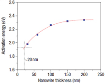
Figure 9. The activation energy varies with nanowire thickness. Higher activation energy implies good retention ability. Reprinted by permission from Macmillan Publishers Ltd: Nature Nanotechnology [17], Copyright (2007).
Download figure:
Standard image High-resolution image3.3. Multi-level cell applications
PCMs can be made to undergo multiple transitions by introducing intermediate resistance states, which is another powerful method to reduce the cost per bit and increase the data density. Feng et al [121] used nanoscale amorphous layers with different resistivities to enable multi-level switching. By manipulating the electrical current and heat, an intermediate controllable state can appear, which can be explained by the formation of crystallites embedded in the bulk amorphous phase, as supported by nucleation theory [122–126].
However, when PCM devices are programmed, the resistance tends to increase over time due to resistance drift, as the amorphous phase tends to increase with time, significantly reducing the memory window of multiple state applications. The defect annihilation model, electron-conduction model and distributed Pool–Frenkel (PF) model have been proposed to explain the origin of resistance drift [33, 127–131]. Thus, physical (stress, temperature) methods or chemical (composition change) methods can be used to design drift-insensitive materials [131]. The thermal disturbance method [87, 124, 132] has also been used to study drift behavior relating to temperature. Nanowire devices [112], different material systems [36, 131] and nanostructure engineering [126, 133] have been used to lower the drift resistance phenomenon due to the reproduction of mechanical and chemical environments.
4. New directions and applications
Despite the knowledge and progress mentioned above, other directions and applications require attention and serve as inspiring representatives of what nanoscale PCMs can offer. The thermoelectric effect, i.e. the conversion of thermal energy into electrical energy, has been studied in PCM materials and devices [134]. The thermoelectric efficiency is characterized by the figure of merit, ZT = σS2T/k, where σ is the electrical conductivity, S is the Seebeck coefficient, T is the temperature and k is the thermal conductivity. Chalcogenide-based PCMs exhibit S ≈ 350–380 µVK−1 [135] and ZT ≈ 0.7 [136]. The metastable pseudo-cubic phase shows planar defects, which were found to drastically decrease the thermal conductivity, possibly by hindering long-wavelength phonon propagation [137, 138]. By additional doping, such as with cobalt germanide precipitates, and forming a 'herringbone-like' structure, a ZT value of 1.7 can be achieved [139], as shown in figure 10. Further optimization of thermoelectric applications might include other types of precipitates. Research has also suggested that the Thomson and Peltier effects could be used to reduce the reset current [135, 140]. In general, the phonon thermal conductivity decreases with decreasing device dimension, resulting in a significant thermoelectric effect and influencing the nanoscale phase-change device properties.

Figure 10. Thermoelectric properties of nanostructure Ge–Sb–Te system of materials. (a) 'herringbone-like structure', contrast due to orientation differences between neighboring domains and twinning. (b) Thermoelectric figure of merit versus temperature change. Different symbols indicate different stoichiometric ratio between Ge–Sb–Te. (a), (b) Reprinted with permission [139] Copyright 2015, American Chemical Society.
Download figure:
Standard image High-resolution imageAnother interesting aspect is the topological insulator system of PCMs. Topological insulators are functional materials with applications, for example, in quantum computers [12, 141]. The topological properties of layered Ge2Sb2Te5 have been predicted by DFT computations for an ideal stacking sequence [142]. The possibility of inducing the TI phase by external force has been discussed [143]. However, the inherent disorder in the ternaries is naturally much higher than that in Sb2Te3, which is the parent material of PCMs and has been proven to be a topologic material [144]. Investigation of the topological nature of the Ge2Sb2Te5 surface has been reported [145], and further investigation is ongoing.
Furthermore, ideas for exploiting the optical properties of PCMs have been reported in recent literature. Color changes in PCM layers can be achieved by manipulating the thickness, which combines both optical and electrical modulation scaling properties [146]. PCMs are also real candidates for all-photonics memory [147]. Recently, a prototype non-volatile memory made of a non-volatile low-dimensional ultra-thin phase-change element integrated with a silicon nitride waveguide was fabricated [148]. An optical application that includes tuning the resonance of an antennae has also been extensively explored [149].
In addition, neuromorphic computing [150, 151] is a promising application of PCMs. In contrast to the 'von Neumann' architecture of today's computer, the neuromorphic system is designed to mimic the computation of the human brain, which is ultra-high density and has low energy consumption and fault-tolerant operation. Here, two nanoscale terminal devices that can emulate the plasticity and energy efficiency of a biologic synapse may be key elements in neuromorphic architecture. Thus, continuous transition between resistance levels is utilized to emulate biological synapses. A successful prototype has been reported [52, 151]. Furthermore, neuromorphic structure devices based on PCMs have been proposed [56–58, 61].
5. Conclusion and outlook
We briefly summarized the properties and applications of nanoscale PCMs and devices. We presented recent results of scaling property analyses of PCMs, including crystallization temperature, melting temperature, crystallization speed, threshold voltage and electrical resistivity. These properties, investigated using separate advanced characterization methods, demonstrate multiple scaling behaviors, most of which are beneficial for device applications and can be manipulated using nanostructure engineering. Recent progress in nanoscale phase-change devices was illustrated. The reset power, endurance properties and multi-level applications were discussed, and some explanations and improvements in these properties were presented. Finally, we presented new applications and directions for PCMs, including various thermoelectric, optical, neuromorphic and topologically insulating applications.
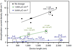
Despite this recent progress, additional effort is still required to explore the limitations and improve the properties of nanoscale PCMs and devices. More precise exploration of the microscopic structure is required. For instance, recent discoveries of microscopic phenomena of PCMs, such as dislocation jamming [29], localization effects [133, 152, 153], strain engineering [154] and interfacial engineering [155, 156], can be guidelines for new designs to improve the performance of PCMs. Thus, a more complex, precisely controlled nanostructure geometry, such as nanowires or superlattices, can be applied to improve the performance [12]. For example, by pre-inducing extended defects through ion irradiation, GeTe-based nanowire devices can achieve ultralow-power switching and show linear trends with an increase in the dimension, as shown in figure 11 [28]. As mentioned above, the interfacial phase-change memory [84, 154] can greatly reduce the switching power as the local structure of the superlattice changes. However, the precise switching mechanism, strain effect and local lattice distortion in the superlattice structure are not fully understood [12, 154, 157]. In addition, for material design of PCMs, a 'treasure map' for finding PCMs was proposed in 2008 and may be extended to other classes of functional materials, which can help in the selection of PCMs [14, 158]. Finally, because different compositions of PCMs are equally desirable, multiple material systems [37, 89, 159] beyond the traditional Ge–Sb–Te system require investigation.
Figure 11. Scaling behavior of phase change nanowires with pre-induced defects at different dosages. Different lines indicate different dosage amount. Reproduced from [28]. CC BY 4.0.
Download figure:
Standard image High-resolution image
The future of nanoscale PCMs and devices is bright, as they continue to evolve and improve through the steady effort of numerous researchers. PCMs are very powerful compounds and will provide a useful material platform for different applications. The success of phase-change devices requires realistic engineering solutions for their special material scaling properties. By continuing to accumulate and explore knowledge of the microscopic properties of PCMs and devices, we believe that exciting treasures will be unearthed in the future.
Acknowledgments
This work is jointly supported by the State Key Program for Basic Research of China (No. 2015CB659300), National Natural Science Foundation of China (Nos. 11621091, 11574143), Natural Science Foundation of Jiangsu Province (Nos. BK20150056, BK20160630), Postdoctoral Science Foundation of China (No.2016M601774), the Project Funded by the Priority Academic Program Development of Jiangsu Higher Education Institutions (PAPD) and the Fundamental Research Funds for the Central Universities.