

Abstract
Electrostatic in-plane microelectromechanical systems (MEMS) relays/switches are widely applied for their low power consumption and simple process. However, compared to the out-of-plane designs, in-plane designs usually suffer from high pull-in voltage, since the feature size of the bulk-silicon process limits the gap between the driving electrodes. Area cost and speed usually have to be sacrificed to enhance the driving force and decrease the pull-in voltage.
Balancing the pull-in voltage, speed and area cost is difficult for MEMS relays/switches but is essential in many practical applications. Comb structure is promising to relieve this contradiction. In this paper, we integrated the comb structure with the cantilever structure. As a result, the pull-in voltage decreased with the decreasing of the mass and area cost. A novel electrostatic lateral MEMS switch was introduced. The experiments have shown that 12 V pull-in voltage, 120  s switching time with a 28 V driving voltage at atmospheric pressure, and small area were fabricated using a conventional bulk-silicon process.
Export citation and abstract BibTeX RIS
1. Introduction
Microelectromechanical systems (MEMS) switches are electrically operated switches demonstrated by micro-fabrication techniques. The specifications of a MEMS switch are almost decided by two key components: the contact [1–3], and the actuator [4–6]. The electrostatic actuators are widely used for their low power consumption [7]. They can be achieved both vertically and laterally. Compared to the out-of-plane actuators [8], in-plane actuators [9] have simpler fabrication process (for fewer lithography steps to define the patterns such as cantilevers and contacts), and also suffer less from the residual stress introduced in the process [10, 11]. Figure 1 shows a schematic view of the lateral MEMS relays.
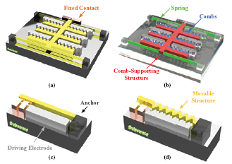
Figure 1. Schematic view of the in-plane MEMS switches. (a) Comb design for low pull-in voltage [12–16, 21], (b) composition of the movable structure in (a) and (c) cantilever design for low switching time [22–24, 30, 31], (d) this work.
Download figure:
Standard image High-resolution imageDecreasing the pull-in voltage and increasing the switching speed are two attractive but contradictory research directions. As shown in figure 1(a), one effective method for the in-plane actuators is adopting a large number of driving combs [12–16]. More combs generate a larger driving force, and the actuator can be pulled-in by lower voltage [13]. The inertia (mass) of the movable structure increases with the number of combs. By optimizing the driving combs [14, 17–21], people can obtain higher driving force and lower pulling-in voltage without increasing the number of the combs. However, the total mass of the movable structure in comb design is much larger than that of the cantilever design (figure 1(c)). Partly the reason is shown in figure 1(b). To use a large number of combs, an additional comb-supporting structure is required. The comb-supporting structure contributes extra mass to the movable structure but does not generate driving force or restoring force. This results in a slow switching speed. The switching time can be decreased by applying a small gap between movable and fixed comb electrodes [19], or, as shown in figure 1(c), by adopting a cantilever design to decrease the mass of the movable structure [22–24]. But some disadvantages have to be taken into consideration. (1) with a smaller gap between movable and fixed comb electrodes, the devices become vulnerable under shock and vibration [25, 26], which are inevitable in the industrial applications. (2) driving force generated by cantilever is not as strong as that generated by the combs as shown in figure 1(a). Two types of driving units, the comb [21], and the parallel-plate, are shown in figure 2, respectively. Furthermore, the driving force of the driving unit can be quantitatively described by equation (1) [27], the definition of parameters are given in table 1.
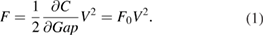
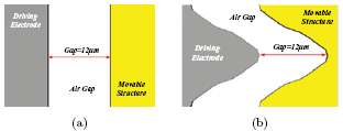
Figure 2. Model of driving units. (a) Parallel-plate; (b) comb [21].
Download figure:
Standard image High-resolution imageTable 1. Definition of parameters in the comb.
| Parameter/unit(SI) | Defination |
|---|---|
| C/F | Capacitance between the fixed driving electrode and the flexible structure |
| Gap/m | Distance between the fixed driving electrode and the flexible structure |
| F0/(N/V2) | Driving efficiency, expressed as  |
The shape of the electrode determines the value of C, under the condition that the dielectric constant and the distance Gap is given. For comb designs, the partial derivative of C versus the distance Gap can be maximized by optimizing the geometry of combs. In this way, the maximum driving efficiency F0 is obtained. As shown in the last column of table 2 [21], the driving efficiency F0 of combs is doubled, compared to the parallel-plate design, at different Gap values.
Table 2. Comparison of F0 between driving units with parallel plate capacitor (F0−Plate) and comb (F0−Comb).
Gap ( m) m) |
F0−Plate (nN V−2) | F0−Comb [21] (nN V−2) |  (%) (%) |
|---|---|---|---|
| 12 | 0.033 | 0.089 | 270 |
| 9 | 0.059 | 0.156 | 264 |
| 6 | 0.133 | 0.303 | 228 |
For the cantilever designs, a lower F0 usually means that a higher voltage is often required for the switch to pull down. To decrease the pull-in voltage, NEMS process [23, 24, 28, 29] or liquid dielectric [30, 31] is necessary. As logic devices, the NEMS are perfect [32–34], but the NEMS devices are hard to be used as power devices to convert tens or even hundreds of milliamperes current [35–37]. Devices with liquid dielectric also have followed disadvantages: (a) they are realized by a complex process, (b) the liquid environment introduces large damping coefficient, which deteriorates the switching time of the relays. For many situations, combs, NEMS and liquid dielectric have similar effects on the MEMS switches: all of them decrease the pull-in voltage. So if combs were adopted, NEMS technology and liquid dielectric are not needed.
In this paper, we present a novel design of lateral MEMS switch. As shown in figure 1(d), we have integrated the combs [21] into the micro cantilever to decrease the mass and area of the device. On one hand, compared to the designs shown in figure 1(a) [12–16, 21], the mass of the movable structure of the device was lower, and the speed response becomes better. On the other hand, compared to the cantilever designs shown in figure 1(c) [22–24, 30, 31], our design could boost the driving force, and obtain lower pull-in voltage.
2. Simulation
To get the static and dynamic characteristics of the switch, we simulated the actuator using finite element method, based on the electro-mechanics interface and solid-mechanics interface of COMSOL®.
Figure 3 shows the models we used in the simulation. Both of the models in figure 3 include (1) the cantilever and (2) the air gap between it and the driving electrode. To facilitate the distinction between different structures, the cantilever is shown in blue, while the air gap is shown in green. Figure 3(a) is the model of design with conventional cantilever design while figure 3(b) is the model of the design in this work. Design of the comb shape was introduced in [21], and parameters of this model are given in table 3.

Figure 3. Schematic view of the simulation models with constrains. (a) Conventional cantilever design, (b) this work.
Download figure:
Standard image High-resolution imageTable 3. Definition of parameters in the simulation model.
| PARM | Defination | Value |
|---|---|---|
| L | Length of the cantilever | 1500  m m |
| W | Width of the cantilever | 12  m m |
| T | Thickness of the structure | 60  m m |
| Gap0 | The initial value of Gap | 12  m m |
| Stroke | The stroke of the contact. In this design, expressed as  |
6  m m |
| ESi | Young's modulus of silicon | 170 GPa |
 |
Poisson's ratio of silicon | 0.28 |
 |
Relative permittivity of air | 1 |
| GND | Ground | 0 V |
 |
Driving voltage | [0 V, 28 V] |
| Ytip | Prescribed displacement on tip of the cantilever (the dark red point in figure 3) | ![$[0, Stroke]$](https://content.cld.iop.org/journals/0960-1317/29/6/065014/revision2/jmmab1635ieqn014.gif) |
| Ftip−re | Reaction force on tip of the can- tilever. Value of it is obtained by the simulator | — |
To simulate the static and dynamic situations of the cantilever under driving voltage, mechanical and electrical boundary conditions are taken into consideration. The key constraints are given in tables 4 and 5.
Table 4. Definition of mechanical constrains.
| Constrain | Color in figure 3 | Location |
|---|---|---|
| Free deformation | Green | Body of the air |
| Linear elastic material | Blue | Body of the cantilever |
| Fixed | Black | Root of the cantilever |
| Prescribed displacement | Dark red | Tip of the cantilever |
| Free | — | Other boundaries of the cantilever |
Table 5. Definition of electrical constrains.
| Constrain | Color in figure 3 | Location |
|---|---|---|
| Electrical material model | Green | Body of the air |
| Electrical potential: VDD | Gray | Boundary of the air |
| Electrical potential: GND | Gray | Boundary of the air |
In this model, prescribed displacement constraint was adopted on the tip of the cantilever. The reaction force is a function of driving voltage and prescribed displacement. Expressed as:

The pull-in voltage, contact force and switching time were obtained in this model by static and dynamic simulations.
2.1. Static simulation
Figure 4 shows the dependence relationship between driving voltage and the displacement of the contact. If the driving voltage is higher than zero, the micro cantilever bends and generates the restoring force. At each voltage, there will be one or more corresponding balance positions. In this balance position, the electrostatic driving force generated by the voltage is the same as the restoring force, and the reaction force on the tip of the cantilever (deep red in figure 3) is 0. If we define the 'balance position' as Ytip−balance, the 'balance positions' of the cantilever tip can be expressed as:


Figure 4. Dependence relationship between driving voltage and the displacement of the contact.
Download figure:
Standard image High-resolution imageThe pulling-in phenomenon has been discussed in several papers [38–43]. The solid circles and hollow squares refer to the balance positions and voltages discussed above. A curve of displacement versus driving voltage is obtained by connecting these points. The position, where the slope of the curve appears to be infinite, is defined as the'turning point' [38]. It is the dividing point between the 'stable points' (solid circles) and 'unstable points' (hollow squares), and the corresponding voltage is the pull-in voltage. The pull-in voltage obtained by simulation is 12 V. And we define the 'contacting force' as Fcontact, the reaction force with driving voltage  and under the condition of the displacement of the cantilever tip is equal to Stroke:

2.2. Dynamic simulation
Figure 5 shows the relationship between switching time and driving voltage, assuming the driving voltage is applied as an ideal step-function in the time domain. Switching time is the time consumption of the tip to move  m. Simulation results show that the switching time would be 105
  s with a 28 V driving voltage and 240
  s with a 12 V driving voltage.

Figure 5. Transient simulation of driving voltage and the displacement of the contact.
Download figure:
Standard image High-resolution image3. Fabrication
The actuator has been fabricated by a conventional bulk-silicon process with 6  m feature size, as shown schematically in figure 6. The silicon structures are bonded on the subtract made of BF33 glass. Initial thickness of the silicon wafer was 300
  m (figure 6(i)). 20
  m height bonding areas were achieved by DRIE process (figure 6(ii)). After the anodic bonding process (figure 6(iii)), the silicon wafer was thinned to 80
  m using the polishing process (figure 6(iv)). Then, 3000
  SixNy was deposited (figure 6(v)) and patterned (figure 6(vi)) to be hard mask. After that, the flexible part was released by DRIE process (figures 6(vii) and (viii)). Finally, 1
  m Cu and 30 nm Au were deposited (figure 6(ix)).

Figure 6. Fabrication process of the actuator. (i) A silicon wafer; (ii) forming the bonding area by DRIE process; (iii) anodic bonding; (iv) thinning by CMP process; (v) SixNy deposition by PECVD; (vi) patterning SixNy by RIE; (vii) flexible part releasing by DRIE; (viii) removing of photoresist and SixNy; (ix) sputtering metal: 1  m Cu and 30 nm Au.
Download figure:
Standard image High-resolution imageFigure 7(a) is the SEM image of the switch, and figure 7(b) is an actuator for pull-in voltage and contact force test.

Figure 7. SEM image of (a)the fully functional switch; (b) the actuator for the contacting force test.
Download figure:
Standard image High-resolution imageWe used an etch protection structure to average the 'local opening density' [44] in both sides of the cantilever. The etch protection structure was also reported in our previous work [45] as restoring force boosting electrode.
4. Experiment
We conducted experiments on both mechanical and electrical characteristics of the device. The experimental setup is shown in figure 8.

Figure 8. Setup for (a) static performance test and (b) dynamic performance test.
Download figure:
Standard image High-resolution imageAs shown in figure 8(a), the micro-robotic system with a force sensor is used to measure the contacting force in the test of static performance. The distance between the force sensor and the micro tip of the actuator is 6  m, which is the same as the stroke of the switch. Thus, if a voltage is applied, the corresponding contacting force is measured. The driving voltage is powered by a DC supply and two DC probes. We use an oscilloscope to sample the voltage between the fixed driving electrode and the micro cantilever.
Figure 8(b) is a schematic diagram of the principle of electrical testing. In the electrical test, we used a fully functional switch as shown in figure 7(a). One static contact of the switch was directly connected to the 6 V DC voltage, and the other was connected to the GND through a  resistor. If the supporting cantilever was pulled in, the movable contact on the tip of the supporting cantilever would become in contact with the fixed contacts, and a current would flow through the resistor and create a voltage drop across it. We used the oscilloscope to simultaneously measure the driving voltage (Voltage I) and the voltage drop across the resistor (Voltage II), to obtain the electrical specifications of the switch. In this way, the pull-in voltage, switching time, and lifetime of the switch were tested.
5. Results and discussion
5.1. Pull-in voltage
Pull-in voltage was obtained by the electronic test. The driving voltage (Voltage I) has risen from zero to 28 V, then gradually decreased from 28 V to 0 V. During the slow rising of the driving voltage, if the device was pulled in, the voltage drop across the resistor (Voltage II) would rise from 0 V to nearly 6 V. The corresponding voltage is the pull-in voltage. Conversely, during a gradual process of decreasing in the driving voltage, if the device was released, the voltage drop across the resistor will decrease from approximately 6 V–0 V. The corresponding voltage is the release voltage.
As shown in figure 9, the pull-in voltage was 12 V and the pull-off voltage was 9 V. The pull-in voltage of this job was even lower to the previous design for low pull-in voltage (14 V) of us [21], and the pull-in voltage of another previous work of us with micro cantilever [46] was 40 V.
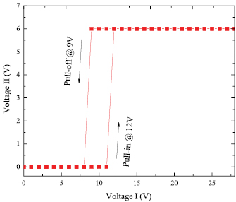
Figure 9. Pull-in voltage test.
Download figure:
Standard image High-resolution image5.2. Contacting force
Contacting force and the structure of contact decides the turn-on resistance [47, 48]. Figures 10 and 11 show the experimental results of contacting force at  m displacement. Figure 10 is the waveform obtained from the micro-robotic system. In figure 11, circles refer to the experimental data and the dashed line refers to the simulated result. The contacting force increases as the drive voltage increases. The simulated result correlates the experimental result well.

Figure 10. Waveform of the contacting force, with driving voltage (a) from 0 V to 12 V; (b) from 0 V to 28 V.
Download figure:
Standard image High-resolution image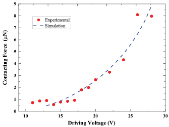
Figure 11. Contacting force versus voltage, at 6  m Stroke.
Download figure:
Standard image High-resolution image5.3. Dynamic performance and life time
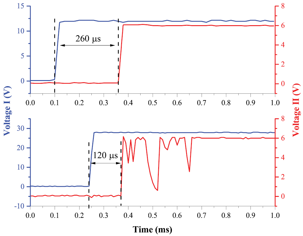
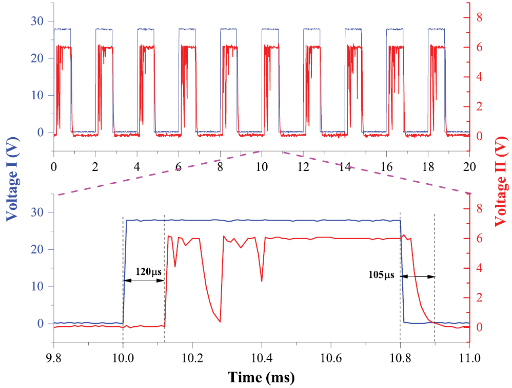
In the dynamic test, the driving voltage was applied as a step-function. Figure 12 shows the waveform of the dynamic test. Blue lines refer to the driving voltage (Voltage I), and the red lines are the voltage drop across the resistor (Voltage II). The switching time can be obtained by measuring the time between the rising edge of the driving voltage and that of the voltage drop across the resistor. Figure 13 shows time-scale waveform with driving voltage of 28 V and 106 cycles. Voltage drops in the beginning of each period indicate the contact-bouncing phenomenon [49–51].
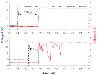
Figure 12. Time-scale waveform with driving voltage of (a) 12 V, (b) 28 V.
Download figure:
Standard image High-resolution image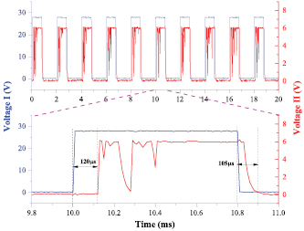
Figure 13. Time-scale waveform with driving voltage of 28 V and 106 cycles.
Download figure:
Standard image High-resolution imageFigure 14 shows the switching time of the device in atmospheric pressure. Red squares refer to the experimental results, and the blue line refers to the simulated results. 120  s switching time was obtained under the condition when the driving voltage is 28 V, and 260
  s switching time was obtained under the condition that the driving voltage is 12 V.

Figure 14. Switching time with different driving voltages.
Download figure:
Standard image High-resolution image
6. Conclusion
A MEMS switch with low pull-in voltage (12 V) and small area (1.5 mm  60
60  m, without pad) is introduced in this paper. The experimental results are in good agreement with the simulation. The switching time was 120
  s with the driving voltage of 28 V at the atmospheric pressure. Compared with our previous works [12, 46], both the switching time and the pull-in voltage were reduced. Since the mass of the movable structure was reduced, the driving efficiency, F0, was improved.
Acknowledgment
This work was financially supported by the National Nature Science Foundation of China, under Grant 61774096.
The authors would like to thank the Tsinghua Nanofabrication Technology Center and Prof Zheyao Wang, the Institute of Microelectronics, Tsinghua University for fabrication support. The authors would also like to thank Dr Yongfeng Gao for the design of combs [21]. Last our thanks would go to Mr Xiangzheng Sun and Mr Jian Chen, the Department of Precision Instrument, Tsinghua University, for testing technique support.