
Abstract
Mechanically flexible interconnects (MFIs) with highly scalable pitch (from 150 to 50 µm) and large vertical gap (65 µm) are reported for the first time in this paper. The wafer-level batch fabrication of the reported MFIs is enabled by photolithography on a highly non-uniform surface (65 µm high sacrificial domes) covered with a spray-coated photoresist. Based on finite element method simulations and experimental data, the mechanical compliance and resistance of the fabricated MFIs are reported.
Export citation and abstract BibTeX RIS
1. Introduction
Flexible interconnect technologies have been investigated over the past two decades for a wide range of applications. Initially, flexible interconnects [1–7] were developed to minimize the thermo-mechanical stress and improve the reliability caused by the coefficient of thermal expansion (CTE) mismatch between assembled silicon dice on an organic substrate. More recently, mechanically flexible interconnects (MFIs) have gained interest in the application of direct assembly of a Si interposer onto a motherboard for lower profile and higher electrical performance [8, 9]. Conventionally, the interposer is mounted on a second substrate (ceramic or organic) before being mounted onto a motherboard [10–14]. But using the MFIs may eliminate the secondary substrate and thus resulting in smaller form factor, higher bandwidth, low energy, and potentially lower cost. These benefits would obviously be attractive in many electronic systems ranging from data centers to mobile electronic applications. The 2012 International Technology Roadmap for Semiconductors (ITRS) [15] projects that the flip chip pitch in mobile products will shrink from 135 µm (in 2012) to 95 µm (in 2026), and the peak package warpage limit, which occurs during solder ball reflow process, to be ±60 µm for the package with solder balls on a pitch of 300 µm. None of the previously reported flexible interconnects can simultaneously provide both a high-density array and a large vertical gap. For example, Kacker et al demonstrated FlexConnects on a 100 µm pitch with approximately 10 µm vertical gap [5]; Spanier et al reported nickel tungsten (NiW) micro-springs with a 40 µm vertical gap and 500 µm pitch [6]. In this work, for the first time, we demonstrate the fabrication and testing of flexible interconnects with 50 µm pitch and 65 µm vertical gap. Therefore, scaling of MFI pitch in conjunction with a large vertical gap enables the reported MFIs to be applicable both as first and second level I/Os.
In addition to being used as permanent interconnects, the proposed NiW MFIs may be applicable for temporary interconnection applications. For example, probe cards used for automated test equipment (ATE) during wafer-level known good die testing can benefit from MFIs.
This paper is organized as following: in section 2, finite element method (FEM) analysis is conducted to investigate the electrical and mechanical properties of MFIs with various pitch and size. The wafer-level batch fabrication process of MFIs with a wide range of dimensions and pitch is discussed in section 3. Finally, in section 4, results from mechanical and electrical testing of the MFIs are reported.
2. MFIs scaling
In this section, we report FEM analysis of the mechanical compliance and electrical resistance of MFIs with various geometries. As shown in figure 1(a), the pitch, p, of an MFI array is the distance between two nearby MFI tips; the length, l, of MFIs is the projected distance between the tip and anchor of the MFI. When the pitch and the length of an MFI are specified, the tapered shape of the MFI is optimized based on the design rules reported previously [7, 9]. Since both the vertical gap and the thickness of the MFI are uniform, they are considered as constant in the analysis reported in this section. The NiW MFI is assumed to be stress-free before deformation because the internal stress induced in the NiW electroplating process [16] is negligible compared to the stress caused by the external bending force. Moreover, the internal stress-free assumption is verified by the fact that the simulated and experimental compliance match as reported in section 4.

Figure 1. Pitch definition (a) and von Mises stress simulations of NiW MFIs on 50 µm pitch (b), 75 µm pitch (c), 150 µm pitch (d).
Download figure:
Standard image High-resolution imageThe mechanical properties of NiW MFIs with various sizes are simulated using ANSYS Workbench 13.0. NiW MFI designs on 50, 75, and 150 µm pitch are shown in figures 1(b)–(d). The MFI thickness and vertical gap are selected as 7.2 and 65 µm, respectively. As shown in figure 1, the inner stress of MFI is uniformly distributed to decrease the maximum inner stress that helps alleviate the mechanical fatigue. The compliance of each simulated MFI is summarized in table 1. The thickness, 7.2 µm, is selected here to optimize the compliance of MFIs on 150 µm pitch. Of course, the thickness of an MFI should be based on a specific MFI geometrical design, which again, in this case was performed for the MFI design with 150 µm pitch. As such, the compliance of the MFIs on 50 µm pitch is lower than those on 150 µm pitch. To increase the compliance of the MFIs on 50 µm pitch, the thickness of the MFIs can be reduced, as shown in figure 2.

Figure 2. FEM simulation results indicate the compliance of MFIs on 50, 75, and 150 µm pitches increases as the thickness decrease.
Download figure:
Standard image High-resolution imageTable 1. Simulation results of MFIs scaling.
| Pitch | |||
|---|---|---|---|
| 50 µm | 75 µm | 150 µm | |
| Length (µm) | 50 | 75 | 150 |
| Vertical gap (µm) | 65 | 65 | 65 |
| Thickness (µm) | 7.2 | 7.2 | 7.2 |
| Compliance (mm N−1) | 1.26 | 2.93 | 5.57 |
| Resistance (mΩ) | 110.63 | 125.72 | 122.48 |
To maintain the tapered design of MFIs, in this work, the size of the MFIs is scaled down in both the x and y directions with the same scaling factor, as shown in figure 1(a). Therefore under such scaling, at a given thickness, the resistance, R, of the MFIs on different pitches does not vary appreciably as demonstrated by the FEM simulation results summarized in table 1.
3. Fabrication process
The fabrication process of the MFIs under consideration is illustrated in figure 3. Conventionally, a spin coating approach is adopted in the fabrication of flexible I/Os with either small pitch (down to 100 µm) or large vertical gap (up to 40 µm), such as the work reported in [1–8]. However, due to two main issues, difficulty to achieve proper exposure of the photoresist and non-uniform evaporation of the solvent (details will be discussed later in this section), spinning coating is not feasible to realize flexible I/Os with both fine pitch and larger vertical gap. In this paper, we utilize conformal photoresist spray coating for the first time, which is the key enabler to scaling MFI pitch to 50 µm, while maintaining a 65 µm tall vertical gap. The fabrication process of the MFIs begins with a sacrificial polymer spin coating on a silicon wafer with a nitride passivation layer. This process step is followed by a thermal reflow process to form 65 µm tall sacrificial polymer domes. Next, a Ti/Cu/Ti film is sputter coated on top of the polymer domes as an electroplating seed layer. Above the seed layer, instead of photoresist spin coating, photoresist spray coating is adopted to realize a 10 µm thick conformal negative photoresist layer (over the 65 µm tall domes). This conformal photoresist layer is patterned and used as the NiW electroplating mold for the MFIs. After electroplating of the MFIs, the photoresist plating mold, the seed layer and the polymer domes are removed leaving behind fine-pitch MFIs with a vertical gap of 65 µm above the substrate. Details of the spray coating process and its advantages over the spin coating for the MFI fabrication process are described next.
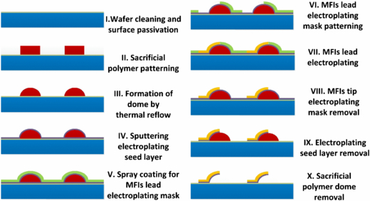
Figure 3. Fabrication process of the MFIs with highly scalable pitch.
Download figure:
Standard image High-resolution imageSpray coating is performed using a Suss Alta Spray Coater (shown in figure 4) to yield a uniform and conformal photoresist film above the polymer domes. During the spray coating process, the diluted photoresist is pumped to a spray nozzle and subsequently pulverized into tiny droplets. These tiny droplets in turn are sprayed out of the nozzle and onto the wafer surface. During the flight from the nozzle to the wafer, most of the solvent in the droplets is evaporated and only the polymer clusters are deposited on the wafer surface to form a conformal film. The spray coater nozzle is scanned in the X- and Y-axes while the wafer is continuously rotated to ensure uniform deposition. The thickness of the deposited film depends on the nozzle scanning speed, the pumping rate, and the photoresist concentration. For example, about 10 µm thick photoresist can be obtained by spray coating diluted negative photoresist with a nozzle speed of 350 mm s−1 and a pump flow rate of 0.8 ml min−1.
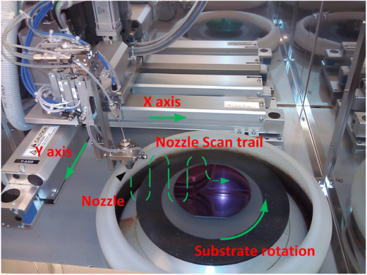
Figure 4. Uniform and conformal photoresist film can be obtained by Suss Alta Spray Coating System.
Download figure:
Standard image High-resolution imageIn order to highlight the key benefits of the spray-coated photoresist layer, a cross-section of sacrificial polymer domes (covered by an electroplating seed layer) coated with a spin-coated and a spray-coated photoresist layer are shown in figure 5. The spin-coated photoresist layer produces a planar surface profile resulting in a non-uniform photoresist layer. Since the photoresist thickness in the spin-coating scenario is non-uniform, two main challenges are introduced that make photoresist spin-coating not applicable for fine-pitch MFIs fabrication: (1) exposure dose control and (2) non-uniform solvent evaporation. However, the surface profile of the spray-coated photoresist layer perfectly follows the wafer surface topology leading to a uniform photoresist layer. In addition, since most of the solvent evaporates during the spray coating process, low temperature soft bake is sufficient for the subsequent photolithography step. Therefore, the two spinning coating induced issues can be perfectly resolved. The challenges induced by spin-coating approach and how they are resolved by spray-coating approach are discussed next.
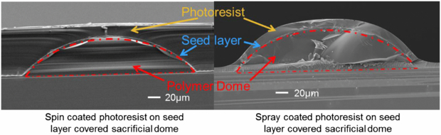
Figure 5. A cross-section examination is performed to compare polymer dome structures coated by the spin-coating and by the spray-coating.
Download figure:
Standard image High-resolution imageAs shown in figure 6, after spin coating, the photoresist layer on the top of the polymer domes is thin while the region in the valley between two domes is thick. The large photoresist thickness difference makes it difficult to achieve proper exposure of the photoresist on both the top of the domes and in the valley between the domes. Either over exposure on the top (resulting in loss of fine patterns) or under exposure in the valley (resulting in severe undercut of MFIs anchor) will render the MFI fabrication as null, as shown in figure 7.
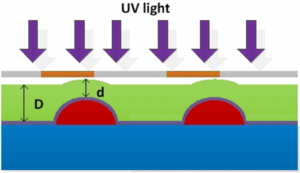
Figure 6. Exposure dose optimization on spin-coated photoresist is difficult due to the non-uniform thickness.
Download figure:
Standard image High-resolution image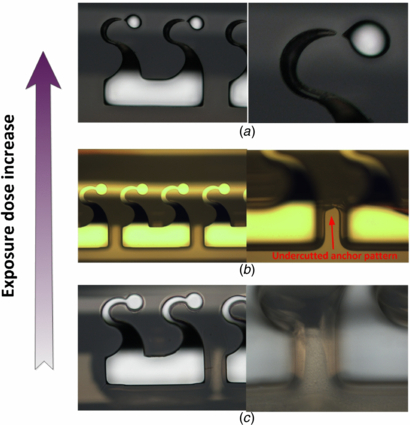
Figure 7. An over exposure of photoresist results in the loss of fine pattern on top of the dome (a); the photoresist undercut cannot be eliminated by a fine-tuned exposure (b); under exposure results in severe undercut in the valley (c).
Download figure:
Standard image High-resolution imageThe other main issue, as shown in figure 8(a), is the non-uniform evaporation of the solvent in photoresist. During the soft bake step, most of the solvent evaporates from the photoresist, which leads to volume shrinkage of the photoresist layer. Due to the thickness variation, the evaporation and the volume shrink are non-uniform, which leads to an inner stress variation around the dome. In addition, the partially melted polymer dome during the high temperature soft bake process step makes the dome prone to distortion. Consequently, the seed layer covering the polymer dome can be broken, which leads to photoresist leakage at the dome edge (figure 8(b)) and seed layer cracking on top of the dome (figure 8(c)). The photoresist leakage will prevent the subsequent electroplating process and yield broken MFIs, as shown in figure 8(d). Moreover, the photoresist plating mold cracking can also be induced by the non-uniform evaporation, as shown in figure 8(e).
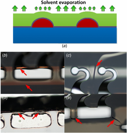
Figure 8. Fabrication issues caused by non-uniform solvent evaporation (a) are: (b) polymer dome leakage, (c) seed layer cracking, (d) MFIs breaking, and (e) electroplating mask cracking.
Download figure:
Standard image High-resolution imageUsing spray coating, a uniform and conformal photoresist film can be formed across the wafer and thus eliminating the two challenges introduced by spin-coating. As shown in figure 9, patterns on top and in the valley of the domes are fully developed with good critical dimension control. Since there is no undercut or breakage in the electroplating mask, shorting is prevented between nearby MFIs after electroplating. Compared with the spin-coated sample, the MFIs fabricated using spray coating avoid the high temperature soft baking therefore the non-uniform solvent evaporation issue and produces MFIs with high yield, as shown in figure 10.
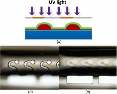
Figure 9. A proper exposure can be conducted on the conformal spray-coated photoresist layer (a). After the development, clear pattern can be obtained both on the top of the domes (b) and in the valley between the domes (c).
Download figure:
Standard image High-resolution image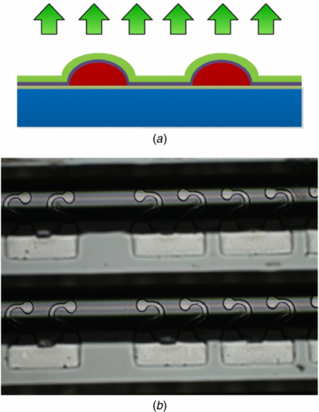
Figure 10. The solvent evaporation of a spray coated sample is uniform with no high temperature soft baking process needed (a) which yields to MFIs consistent to design geometry on the dome surface with no cracks (b).
Download figure:
Standard image High-resolution imageAfter the removal of the plating mold, seed layer, and sacrificial domes, figure 11(a) illustrates the remaining free standing MFI array with various pitches (150, 75 and 50 µm). The 65 µm vertical gap of MFIs is verified by the side view, as shown in figure 11(b). High magnification images of MFIs with various pitches are illustrated in figure 12. All MFIs have the same vertical gap (65 µm) and thickness (7.2 µm).
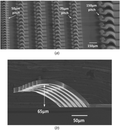
Figure 11. Overall view (a) and side view (b) of free standing MFIs array on 150, 75 and 50 µm pitch with 65 µm vertical gap.
Download figure:
Standard image High-resolution image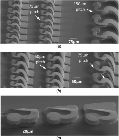
Figure 12. High magnification images of MFIs with various pitch.
Download figure:
Standard image High-resolution image4. Results and discussion
In this section, mechanical indentation and electrical four-point resistance measurements are reported for 7.2 µm thick MFIs on 50, 75 and 150 µm pitch.
4.1. Mechanical indentation test
Indentation testing of the MFIs is carried out by a Hysitron TriboIndenter. As shown in figure 13, for each indentation cycle, the free standing MFI is deformed downward to a preset depth under a predefined force profile applied by a piezo-driven indentation head. After indentation, the MFI is released to recover its original (pre-indentation) profile. The real-time position and corresponding reaction force of the tip, which has the same value as that of the MFI tip, are recorded.
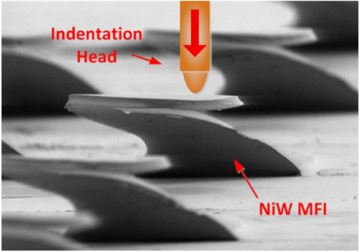
Figure 13. Mechanical indentation test performed on MFI. The freestanding MFI is deformed by a piezo-driven indentation head.
Download figure:
Standard image High-resolution imageAs shown in the indentation results of figure 14, there are two loading steps in each indentation cycle: a forward loading step and a backward loading step. During the forward loading step, the MFI is pressed downward, while the applied force and the position of the deformed MFI are recorded as the forward plot. Similarly, the backward plot is recorded during the backward loading step while the MFI attempts to recover its original position.
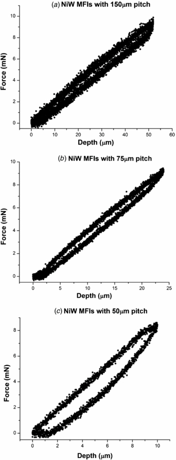
Figure 14. Indentation test results of MFIs on (a) 150 µm pitch, (b) 75 µm pitch and (c) 50 µm pitch.
Download figure:
Standard image High-resolution imageThe results of the 150 µm pitch MFIs are shown in figure 14(a). The measured reaction force is 9.4 mN for a 50 µm vertical deformation resulting in a measured compliance of 5.32 mm N−1. For the 75 µm pitch MFIs, the indentation results are shown in figure 14(b), and the measured reaction force is 9.2 mN at 25 µm vertical deformation, resulting in a compliance of 2.72 mm N−1. For the 50 µm pitch MFIs (figure 14(c)), the measured reaction force is 8.3 mN at a 10 µm vertical deformation, resulting in a compliance of 1.20 mm N−1. These results are summarized in table 2 and consistent with our FEM simulations in section 2. Again, to increase the compliance of the MFIs on the smaller pitch, a thinner metal film should be electroplated as shown in figure 2.
Table 2. Comparison between FEM simulation and experimental data.
| Pitch | |||||
|---|---|---|---|---|---|
| 50 µm | 75 µm | 150 µm | |||
| Compliance (mm N−1) | FEM simulation | 1.26 | 2.93 | 5.57 | |
| Indentation measurement | 1.20 | 2.72 | 5.32 | ||
| Resistance (mΩ) | FEM simulation | 110.63 | 125.72 | 122.48 | |
| Four point | Average | 119.1 | 134.3 | 133.2 | |
| measurement | |||||
| Standard | 3.87 | 4.02 | 3.79 | ||
| deviation | |||||
4.2. Electrical resistance test
The four point electrical resistance measurement is performed by a Signatone Probe Station. As shown in figure 15, two probe tips are placed on the tip of the MFI and another two probe tips are placed on the anchor of the MFI. During the measurements, the tested MFIs are partially bent to attain a stable resistance reading. Seven MFIs were randomly picked from each of the three designs with different pitches. As plotted in figure 16, the average resistance of MFIs on 150, 75 and 50 µm pitch is 133.2, 134.3 and 119.1 mΩ respectively. The resistance is slightly larger than the results from FEM simulations, which is believed due to the fact the resistivity of the electroplated metal film is higher than that of bulk material, which is used in the simulation.
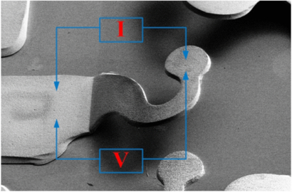
Figure 15. Four-point resistance test on MFIs.
Download figure:
Standard image High-resolution image
Figure 16. Four-point resistance test results for 50, 75 and 150 µm pitch MFIs.
Download figure:
Standard image High-resolution image
5. Conclusions
The mechanical compliance and electrical resistance of 7.2 µm thick MFIs is investigated using FEM simulations, and results were experimentally verified. The key features introduced in this paper are: (1) a spray-coating assisted process has been developed to enable fine pitch patterning on a substrate with a large surface variation; (2) MFIs with highly scalable pitch (from 150 to 50 µm), and large vertical gap (65 µm) have been obtained for the first time; and (3) electrical and mechanical properties of the MFIs with various pitch are investigated through FEM simulations and experimental testing.
Acknowledgments
This work is supported by Oracle Labs. Special thanks for the invaluable discussions with Dr James Mitchell, Dr Hiren Thacker, and Dr John Cunningham at Oracle Labs.