

Abstract
By exploiting the interesting trait of graphene to have electrically tunable first- and third-order conductivities besides its capability to support plasmonic resonances at terahertz frequencies, here, through the nonlinear finite-difference time-domain numerical technique we developed, we demonstrate a noticeable improvement in the conversion efficiency of third-harmonic generation (THG) from a graphene microribbon array by more than five orders of magnitude compared to an infinite graphene sheet, under normal illumination of terahertz waves. As the Fermi level and period length of the ribbon array increase, the transmission obviously manifests a blue shift but denotes a red shift with an increase in ribbon width. The quality factor of resonance (and so the THG efficiency) also shows improvement with an increase in graphene Fermi level, carrier mobility and period length and is degraded by an increase in ribbon width. Generating new frequencies, terahertz signal processing, spectroscopy and so on are among the plethora of valuable potential applications envisioned to be developed based on the findings reported here.
Export citation and abstract BibTeX RIS
1. Introduction
While it is believed that the universe is bathed in terahertz (THz) energy, and myriad applications in chemical and biological imaging, security technology, and astronomy are envisioned for the THz frequency range (roughly from 100 GHz − 10 THz), until relatively recently, it has remained one of the least tapped regions of the electromagnetic spectrum compared to its neighbors (the infrared and microwave bands) due to lack of efficient laboratory facilities such as emitters, detectors and so on. Since a large number of materials are transparent for THz waves, the development of THz technology and the implementation of THz components require materials with proper response to THz frequencies [1, 2]. Although metamaterials have been proven to offer a promising approach for this dilemma, the complexity in design and difficulty in the fabrication process have remained obstacles. Graphene, a recently isolated two-dimensional crystal of  carbon atoms, arranged in a honeycomb lattice, is a material of interest in this context. Over the last few years, whole ranges of experiments have revealed the fascinating electrical, optical and physical properties of graphene, mainly originated from its exceptional Dirac cone-type band structure [3–5].
While in the conventional plasmonics of noble metals there is no opportunity for efficient excitation of surface plasmon polaritons (SPPs) at the THz band and it is limited to the study of transverse magnetic (TM) SPPs at the near infrared and visible frequencies, graphene can support either TM or transverse electric (TE) SPPs depending on the sign of the imaginary part of its conductivity. TM plasmons in graphene offer a higher level of confinement, a lower degree of loss and therefore greater propagation length than their metal counterparts. TE plasmons are also specified by low loss even in room temperature but weak localization at the surface [6–9]. The strong coupling of light to SPPs and the consequent creation of strong localized electromagnetic fields and the high sensitivity of SPPs to the properties of the dielectric bounding medium, besides the fast response time of plasmonic excitations, which can strengthen the traditionally observed nonlinear phenomena in bulk semiconductors, make plasmonics a good platform for nonlinear studies [10]. The nonlinear plasmonics field includes both the nonlinear response of the dielectric environment and the active medium such as noble metals. Although the nonlinear response of metallic films and nanostructures is thoroughly investigated in the visible and near infrared frequencies, it cannot be extended to the THz regime since noble metals cannot effectively support SPPs at these frequencies. The limitations of noble metal based plasmonics can be effectively addressed by graphene, a material of atomic thickness. The capability of graphene to support SPPs at THz frequencies combined with its dynamically tunable, strong nonlinear response due to the particular linear energy dispersion of its charge carriers nominates graphene as a promising candidate for the relatively unexplored field of THz nonlinear plasmonics. The particular nonlinearity of graphene is theoretically predicted in [11–14] and experimentally confirmed in several cases including direct measurement of the third-order refractive index with the Z-scan technique [15], observation of four-wave mixing in graphene flakes [16], and third-harmonic generation (THG) [17].
Over the last few years, some aspects of graphene nonlinearity have been reported in the literature including its bistability [18], Kerr nonlinearity [19], self-induced regenerative oscillations [20], four-wave mixing [16, 20], second-harmonic generation (SHG) [21, 22], saturable absorption [23], THG [17] and soliton formation [24] with applications in SPP wave excitation [25, 26], phase shifting [27], filtering [28], switching [29], ultrafast pulsed lasers [30] and so on. In this contribution, we aim to study the enhancement of THG from graphene sheets under normal illumination of THz waves due to plasmon resonance. While in our recently published paper, we have investigated the effect of the quasi phase matching technique to enhance the efficiency of THG for propagating SPPs on graphene [31], here we show how patterning graphene as a microribbon array can considerably promote the efficiency of THG by several orders of magnitude due to plasmonic interactions, compared to infinite graphene sheets under normal illumination of THz waves. Although resonance-enhanced THG via azo-polymer resonant waveguide gratings [32], optical fibers [33], Ag nanoparticles [34] and film-coupled plasmonic strip resonators [35] has been studied in the visible and near infrared frequencies, the use of graphene due to its capability of supporting plasmonic modes in the THz band gap (providing opportunity to work below the diffraction limit), its large third-order nonlinearity (reducing power consumption for a given nonlinear response) and the gate voltage tunability of its first- and third-order conductivities introduces fascinating aspects to this topic, worthy of exploring. This is besides the atomic thickness and planar nature of graphene, which make it a promising candidate for miniaturized and highly integrated nonlinear THz plasmonic devices and circuits.
The current study presents the extension of the nonlinear plasmonic field to the THz regime. Here, for the first time to our knowledge, we reveal a noticeable enhancement in the conversion efficiency (CE) of dynamically tunable THG over the THz gap due to plasmonic resonance from a graphene microribbon array of nanometer thickness, which cannot be achieved by conventional noble metal based plasmonics.
Since graphene is a two-dimensional centrosymmetric crystal, SHG in it is prohibited [36]. However, in some particular cases, symmetry breaking achieved by fabricating nanoislands of graphene with finite size [37] or by an oblique incidence of radiation on infinite graphene sheets [21] can lead to SHG from graphene which is outside of the focus of this study.
2. Graphene conductivity
Within random phase approximation and in the absence of a magneto-static bias field and spatial dispersion (where the conductivity components become wavenumber dependent), the graphene isotropic complex surface conductivity can be expressed as (assuming  time harmonic dependency) [38]:
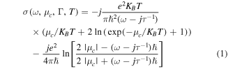
where the first and second terms refer to the intraband and interband graphene conductivities originated from the intraband and interband transitions of electrons respectively. In this relation -e is the electron charge,  is the reduced Planck's constant,
  is the angular frequency,
  is the electron–phonon relaxation time, T is the temperature,
  is the Boltzmann constant,
  is the chemical potential representing the graphene Fermi level, and
  is the energy. The interband term in this relation is calculated approximately by considering the constraint of
  For frequencies
  the graphene conductivity is dominated by the interband transition of electrons which is known as a major mechanism of plasmon loss (via excitation of electron–hole pairs) [6, 38]. Furthermore, in this frequency range the sensitivity of graphene conductivity to the Fermi level and frequency is negligible and has a universal value of
  for
for  corresponding to a noticeable absorption constant of 2.3% per graphene layer with atomic thickness [39–41]. On the other hand, for frequencies
  the Pauli principle will block interband transitions (in p-doped graphene there is no electron available for the interband transition and in n-doped graphene electron states in resonance in the conduction band are occupied) and the intraband transition of electrons (free carrier absorption) plays a significant role. In this frequency range, which is considered as a low-loss regime (the real part of conductivity is much smaller than the imaginary part) for graphene operation, the graphene conductivity reveals great tunability with the Fermi level [38, 42].
The nonlinear conductivity of graphene is also defined as [11, 12, 43]:

In the low-frequency limit, where  the interband transition of electrons occurs at a negligible rate compared to the intraband one and the third-order conductivity of graphene is proportional to
  In contrast, for higher frequencies where
  the interband transition of electrons plays the dominant role and the frequency dependency of third-order conductivity would be proportional to
  according to quantum mechanical analysis [16, 28]. The coefficient
  in (2) represents the effect of two-photon absorption (TPA) in graphene which in recent experiments is shown to be
  [20, 43]. Since TPA is essentially an interband mechanism and we work in low THz frequency on moderately doped graphene samples in which the intraband transition of electrons has the dominant role besides the smallness of the real part of the graphene nonlinear conductivity compared to its imaginary part and also for numerical simulation simplicity, we ignore the effect of TPA in graphene in our study.
Our simulations are performed in room temperature  and the electron–phonon relaxation time is calculated as
  [44] where
  is the Fermi velocity and
  is the mobility of charge carriers taken in the order of
  in our simulation corresponding to
  for
for  which is a rather large value for graphene samples on a substrate in room temperature (while an ordinary one for suspended graphene sheets in low temperatures and also reported in several works for fabrication under special conditions for the lowest level of impurities, with multilayer structures or with special types of dielectric environments) [45–47]. This is only by considering the graphene operation in the nonlinear regime in our study. Actually for lower typical values of relaxation time in the order of 0.1 ps graphene loss would be noticeable and to work in the nonlinear regime, high and possibly unachievable light intensities may be required. In this regard, for nonlinear purposes, low-loss and high-quality samples are preferred.
3. Numerical method
To investigate the THG capability of graphene, schematically illustrated in figure 1(a), and calculate the power transmission, we employ a subcell finite-difference time-domain (FDTD) numerical technique which can precisely model the atomic thickness of graphene. Taking the assumption that the graphene sheet is infinite and invariant in the y direction, the simulation can be performed in a two-dimensional case, according to figure 1(b), without loss of accuracy. Certainly, more accurate results by accounting the effect of finite length in this direction can be accomplished by three-dimensional subcell FDTD but at the cost of a large amount of computer memory and computing time. The periodic boundary condition is enforced to the x direction to simulate the periodicity and infinity and the convolutional perfectly matched layer (CPML) is employed in the z direction to dissipate the outgoing waves [48–51]. The number of CPML cells is set to be 80, to ensure the complete absorption of power at the boundaries. The FDTD grid size is chosen as  [52] (the results for a smaller grid converge to the analytic ones). The time step is also set following the Courant stability condition
 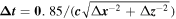 [51], where c is the speed of light in the free space (according to our numerous simulations, our developed code is stable). We recall that by working in the frequencies
  only the intraband transitions of electrons would be relevant and only this term of graphene linear and nonlinear conductivities should be included in the FDTD code.
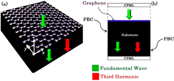
Figure 1. Schematic of (a) THG from extended graphene sheet relying on a flat substrate and (b) two-dimensional simulated structure via FDTD (the effect of the finite thickness of the substrate and possibly related Fabry–Perot resonances are ignored in our study).
Download figure:
Standard image High-resolution imageBy defining a volume conductivity for a  thick graphene layer as
  the volume current density and thus Ampere's law can be written as
  and
and  respectively. So we can ascribe an equivalent complex permittivity of
  and thus an equivalent effective linear susceptibility of
  to the
  thick graphene layer where
  and
and  denote the real and imaginary parts of graphene conductivity [53, 54]. In the same way, an equivalent nonlinear susceptibility can be designated to graphene defined as
  [55, 56].
Although it seems that the more appropriate implementation of graphene as a two-dimensional material in the FDTD code would be by its linear and nonlinear conductivities (and so by its linear and nonlinear currents), the bulk representation of graphene (certainly of finite thickness) by its linear and nonlinear susceptibilities (and so by its linear and nonlinear polarizations) in this study is only due to the presence of a Kerr-nonlinear medium in the graphene environment which must be modeled by polarization.
By working in the frequency range where only the intraband term of graphene conductivity is relevant, the effective linear susceptibility can be written as [50, 51]:


where a is the portion of the cell occupied by graphene which in our simulation is taken to be 0.01 (the graphene thickness is taken to be 1 nm). However it is shown that inasmuch as the graphene thickness is sufficiently small compared to the working wavelength, this special choice is not of critical importance [53].
To simulate the spectral response of the system and evaluate its THG capability, Maxwell's equations are solved by using an FDTD algorithm. For this purpose, at first electric flux density D is calculated using a discrete form of Ampere's law (in the time and space domains)  where H is the magnetic field vector. The key point to model graphene in our FDTD code is in the next step by use of the following constitutive relation [48]:

in which we have assigned the linear polarization of  and the nonlinear polarization of
  to characterize the linear and nonlinear dispersive nature of graphene and the nonlinear polarizations of
  to describe the Kerr-effect of the graphene bounding medium. The relations used to incorporate
  and
and  in our FDTD code can be found in [50, 51] and
  is implemented as a fourth-order time-derivative (considering the
  frequency dependency of
  following the procedure reported in [48, 57]. A Newton iteration technique is applied to find the electric field from equation (7). Finally, the magnetic field can be computed by a discretized expression of Faraday's law
  where
where  is the magnetic permeability.
Throughout this work, we employ light of TM polarization in normal incidence (the electric field is in the x direction and along the width of the ribbon). This condition is necessary to excite TM SPPs in the following explored resonant structures (if the incident electric field is oriented along the length of the ribbon instead of the width, no resonance is observed since the ribbon is too long to support any resonance in our working frequency range besides that by considering the sign of the imaginary part of graphene conductivity; for the chosen graphene Fermi levels in this study and also our working frequency range, the graphene can only support TM SPPs). To study THG, a cosine-modulated Gaussian wave packet centered at the frequency of the fundamental wave (FW), narrow in the frequency domain and thus long-standing in the time domain, is launched to the structure (along a line in the x direction on one side of the structure) which requires a rather large computational box. Certainly to calculate the transmittance, reflectance and absorbance spectra over a wide spectral range, the illuminated Gaussian wave should be sufficiently broadband (wide in the frequency domain and narrow in the time domain). Our excitation source can be expressed mathematically as  where
where  is the time in the FDTD loop,
  is the amplitude,
  is the center frequency,
  is the time delay and
  determines the pulse width in the time and frequency domains.
To compute the transmitted power  the structure (infinite graphene sheet or ribbon array) is excited from one side (e.g. the top of the structure) and the FDTD calculated fields are recorded over a line (along the x direction) on the other side (e.g. the bottom of the structure). By taking the fast Fourier transform from the recorded fields and integrating the pointing vector over the sampling line,
  can be calculated. Removal of the structure (a situation in which the medium in the simulation region is homogenous and no reflection occurs) is done to calculate the incident power
  The normalized transmitted power is defined as
  Sampling for the reflected power
  is performed on the same side of the excitation and the difference in calculated power in the presence and absence of the structure gives
  .
.
All of our simulations are performed by exploiting the C++ programming language and MATLAB software on a P4 Core(TM)2 Quad CPU 3 GHz with 8 GB RAM. In the THG study, more than 300 000 time steps (corresponding to 260 min running time) are considered, and in the calculation of transmittance, reflectance and absorbance spectra, around 80 000 time steps (corresponding to 70 min running time) are taken into account.
To validate the FDTD code we developed, the normalized transmitted (T), reflected (R) and absorbed (A) powers for the normally incident light wave upon an extended graphene sheet are computed and the results are compared with the analytic solutions defined as [49]:


where  and
and  refer to the regions above and below the graphene sheet. The result of this comparison, which is depicted in figure 2, confirms the accuracy of our code. (The effect of the finite thickness of the substrate and possibly related Fabry–Perot (FP) resonances are ignored here).

Figure 2. Comparison of normalized (a) transmitted, (b) reflected and (c) absorbed power computed by FDTD with analytic solution for the case where a light wave normally illuminates an extended graphene sheet. The results are for two different graphene Fermi levels and two different substrates (air with relative permittivity of 1 and silicon (Si) with relative permittivity of 11.9).
Download figure:
Standard image High-resolution imageWe have also examined our code in the case of SPP wave propagation on a graphene sheet. For this purpose the frequency and Fermi level dependency of the wavelength of the propagating TM SPP wave are computed by the dispersion relation according to [6]
and are compared with the ones obtained from our FDTD code where  and
and  are the relative dielectric constant of the surrounding medium,
  is the plasmon wave vector and
  is the free space light speed. The results show very good agreement as depicted in figures 3(a) and (b) respectively. The inset in figure 3(b) shows the spatial distribution of
  in the x–z plane in the steady-state case for a suspended graphene sheet at the frequency of 5 THz and
  .
.
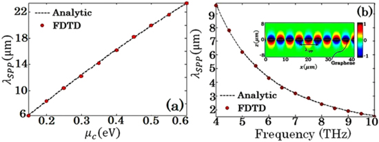
Figure 3. Comparison of  extracted from FDTD code and (11) (a) at the frequency of 5 THz and (b)
  The inset shows the spatial distribution of
  in the x–z plane in the steady-state case for a suspended graphene sheet at the frequency of 5 THz and
  .
.
Download figure:
Standard image High-resolution image4. THG from infinite graphene sheet
Figure 4 shows the normalized output power (the output power is normalized to the incident power at the FW) for the case depicted in figure 1. Here the intensity of the FW is  and the graphene Fermi level is set as
  The first peak is attributed to the excitation of the structure with a narrowband, cosine-modulated Gaussian wave packet for which the center frequency is taken to be the frequency of the FW and here is set at 0.5 THz. While for low-intensity illumination there is no second peak in the output spectrum, by increasing the illumination intensity a peak appears at the place of the third harmonic (TH) (1.5 THz) due to third-order nonlinearity in the graphene and its substrate (in fact there is no direct excitation at TH). The substrate chosen is
  glass as a Kerr-nonlinear medium, with a linear refractive index of 2.86 and a nonlinear refractive index of
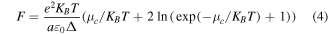
  in the THz regime [58]. This Kerr-nonlinear substrate is taken to be isotropic, homogenous and dispersionless over our frequency range. In what follows, to have a concept of THG strength, we evaluate the CE defined as
  where
where  and
and  stand for the produced TH power by graphene and the incident pump power at the FW respectively. The CE for the result presented in figure 4 is obtained around −80 dB.

Figure 4. The normalized output power spectrum for the extended graphene sheet with  relying on
  glass under normal illumination with FW intensity of
 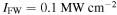 and FW frequency of
  .
.
Download figure:
Standard image High-resolution imageTHG from the graphene sheet under normal illumination is mainly affected by three factors. According to (2) stronger nonlinear response is expected for graphene layers of lower Fermi level. This is mainly due to the fact that for operations in the nonlinear regime, the total energy gained by electrons in graphene under high intensity illumination should be high enough compared to their average Fermi energy. The intensity of the FW  is also a key factor that largely contributes to THG efficiency. While for lower FW intensities the response of the system is linear, for higher ones it enters the nonlinear regime and higher values of THG efficiency are obtained. Finally, the frequency of the FW
  is considered as an influencing factor. According to (2), the graphene third-order conductivity is higher at lower frequencies so a higher TH level is expected for operation in this region. Figure 5 shows how CE varies with these three factors.
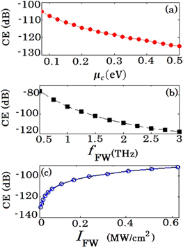
Figure 5. CE versus (a) graphene Fermi level for  and
and  , (b)
, (b)  for
for  and
and  and (c)
  for
for  and
and 
Download figure:
Standard image High-resolution imageWhile for lightly doped graphene samples under illumination of low-frequency THz waves the contribution of graphene in THG is dominant and THG from a Kerr-nonlinear substrate is negligible, for heavily doped graphene samples under high-frequency THz wave illumination, the graphene nonlinear response becomes weak and comparable with that of the substrate. Certainly, this fact cannot be overlooked that to get a nonlinear response from graphene samples of a high Fermi level with higher frequency of the FW, the intensity of illuminating THz waves should be increased which in turn enhances the contribution of the substrate in THG. This phenomenon is explored in figure 6.
Figure 6. Comparison of graphene and substrate contribution in THG for (a) 
 and
and  , (b)
, (b) 
 and
and 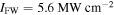 and (c)
 and
and  .
.
Download figure:
Standard image High-resolution image5. Resonance-enhanced THG from graphene microribbon array
In what follows, we investigate how plasmonic interactions by creating a strong localized electromagnetic field may help to improve the efficiency of THG from graphene under normal illumination of THz waves. For this purpose, we investigate a periodic array of graphene microribbons, as depicted in figure 7.
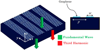
Figure 7. Schematic of THG by graphene microribbon array.
Download figure:
Standard image High-resolution imageThe resonance condition in the normal illumination of the graphene microribbon array, depicted in figure 7 (as far as the coupling strength between the ribbons would be negligible, especially for arrays with periodicity sufficiently greater than the ribbon widths), is achieved following the excitation of SPPs in each ribbon where a constructive interference occurs for an SPP round trip [59]:

where  is the propagation constant of the SPPs, m is an integer (the first resonance can be determined by placing
  , Re indicates the real part,
  is the ribbon width and
  is the phase induced upon reflection at the ends of the ribbon, commonly taken to be
  based on the assumption that the field vanishes at the ribbon edge. However, considering the complex excitation of deeply evanescent modes near the ribbon edges and imposing the continuity of electric and magnetic fields leads to a nontrivial phase of about
  which is essentially independent of the intrinsic properties of graphene (Fermi level, temperature....), the wavelength of operation, and the dielectric environment, and strongly affects the resonant frequencies [50, 59].
Figure 8 shows the transmittance (T), reflectance (R) and absorbance (A) spectra for the schematically depicted case in figure 7 under normal illumination of low-intensity THz waves with 
 and
and  and a silicon substrate of
  at THz frequencies [60]. Consistent with our expectation, a notch in the transmittance spectrum and a peak in the reflectance and absorbance spectra at the resonant frequency are created due to the excitation of SPPs. Charge accumulation along the edge of the graphene ribbon may affect its local conductivity which for the sake of numerical simulation simplicity is not taken into account in our study; however, including this effect may lead to more realistic results [61].
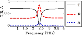
Figure 8. Transmittance, reflectance and absorbance spectra for schematically depicted case in figure 7 under normal illumination of low-intensity THz waves with 

 and
and  .
.
Download figure:
Standard image High-resolution imageFigure 9(a) shows the FDTD calculated transmittance spectra for different values of the graphene Fermi level with 
 and a silicon substrate of
  Figure 9(b) illustrates that the resonant frequency undergoes a blue shift with an increase in Fermi level due to a reduction in the
  of the excited SPPs following equation (12) [50, 51]. The resonant frequencies obtained from our FDTD code reveal very good agreement with those obtained from equation (12). The quality factor
  of resonance shows an increase with the graphene Fermi level as depicted in figure 9(c). This is mainly attributed to the higher resonant frequency and also an increase in the figure of merit (FOM) of propagating SPPs on graphene defined as
  [31]. The reduction in minimum transmittance at the resonant frequency with an increase in graphene Fermi level is also attributed to the higher number of charge carriers contributed in the plasmonic oscillation [62]. Besides that, the minimum transmittance is strongly affected by the value taken for the mobility of the charge carriers. In fact, for lower-quality graphene samples (with lower mobility of charge carriers), the loss is more noticeable and the minimum transmittance (the quality factor of resonance) increases (decreases).
Figure 9. (a) Transmittance spectra of structure in figure 7 for various graphene Fermi levels under normal illumination of low-intensity THz waves with 
 and
and  and (b) resonant frequency and (c) quality factor versus graphene Fermi level.
Download figure:
Standard image High-resolution imageIt is well known that a change in graphene Fermi level can be achieved by chemical doping or applying a gate voltage between a Au electrode on graphene and a highly doped silicon substrate which can act as a bottom electrode while an insulating layer, typically silicon dioxide  is positioned between the graphene and silicon substrate. However, in this study, we have ignored the finite thickness of the substrate and related FP resonances. Certainly, the coincidence of the frequency of FP and plasmon resonances and the proper positioning of the graphene microribbon array at the place of maximum field enhancement in the FP cavity (or even the coincidence of FP resonance with the TH) may help to increase the TH level which is not the subject of the current study.
Following equation (12) a red shift in the resonant frequency by increasing the ribbon width is expected. Figure 10(a) shows the transmittance spectra for different values of the ribbon width while the graphene Fermi level and period of the array are kept constant at  and
and  respectively. The relation reported in equation (12) is valid for single ribbons or arrays of periodicity much greater than the ribbon width. By matching the ribbon width to the period of the array due to an increase in coupling strength between adjacent ribbons, the resonant frequency undergoes a red shift compared to a single ribbon and the quality factor of resonance also shows a reduction. The reduction in quality factor with an increase in ribbon width may also be attributed to the lower resonant frequency besides the lower FOM of the SPP mode at these frequencies. Figures 10(b) and (c) respectively explore the variation of resonant frequency and the quality factor with ribbon width.
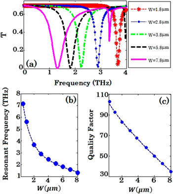
Figure 10. (a) Transmittance spectra of structure in figure 7 for various ribbon widths under normal illumination of low-intensity THz waves with 
 and
and  and (b) resonant frequency and (c) quality factor versus ribbon width.
Download figure:
Standard image High-resolution imageWe also investigate how the period of the array can affect the resonant frequency and quality factor of resonance without any change in the graphene Fermi level and ribbon width. Figure 11(a) depicts the transmittance spectra for different values of the period at 
 and
and  The variation of resonant frequency and the quality factor with the array period is also illustrated in figures 11(b) and (c) respectively. Consistent with our discussion above, by increasing the period (and thus the inter-ribbon space) the resonant frequency approaches the value of a single ribbon and the quality factor of resonance also increases due to the higher resonant frequency and greater confinement of the SPP mode.
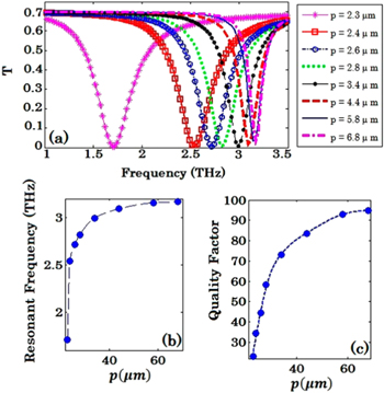
Figure 11. (a) Transmittance spectra of structure in figure 7 for various periods of the array under normal illumination of low-intensity THz waves with 
 and
and  and (b) resonant frequency and (c) quality factor versus ribbon width.
Download figure:
Standard image High-resolution imageNow let us investigate how the resonance in the above investigated graphene microribbon array can enhance TH strength. We expect in the case of the coincidence of the resonant frequency with the FW frequency, the localization of the electric field around the graphene ribbon, which boosts the nonlinear response of the structure arising from both the graphene and the nonlinear substrate, leads to considerable improvement in CE. To show the effectiveness of patterning graphene as a microribbon array and the influence of different parameters on the improvement of the THG CE, we define  which compares the CE obtained by the graphene microribbon array denoted by CERA with a reference case of an infinite graphene sheet denoted by CEIN (schematically depicted in the insets of figures 12(a) and (b) respectively). To study each parameter, other parameters involved in both cases (including the intensity and frequency of the illuminating wave and other structural and graphene parameters) are taken to be the same.
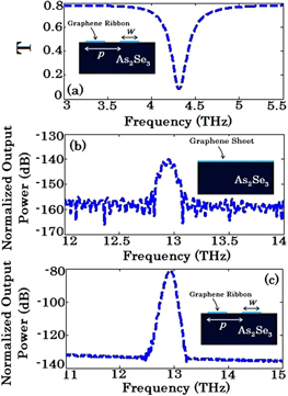
Figure 12. (a) The transmittance spectrum for a graphene microribbon array of 
 and
and  positioned on a substrate made of
  glass under normal illumination. Normalized output power for (b) infinite graphene sheet and (c) microribbon array under normal illumination with
  and
and  (the insets show the unit cell of the studied structure).
Download figure:
Standard image High-resolution imageFigure 12 explores this fact. The transmittance spectrum for a graphene microribbon array of 
 and
and  on a substrate made of
  glass is depicted in figure 12(a) which shows a resonance around
  This resonant frequency is chosen as
  For the infinite graphene sheet a very low TH level with noiselike behavior for
  is observed according to figure 12(b), by patterning it as a microribbon array; interestingly, the TH level at the same
  and
and  is increased by around six orders of magnitude.
According to our discussion above, increasing the graphene Fermi level and period of the array and reducing the ribbon width lead to resonances of a higher quality factor and hence a field enhancement on the graphene which is expected to improve the efficiency of THG. This expectation is confirmed by our FDTD simulation results depicted in figures 13(a)–(c) respectively.
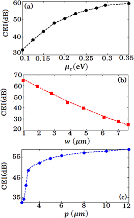
Figure 13. Improvement in the conversion efficiency of THG by pattering graphene as an array of microribbons compared to an infinite graphene sheet while both of them are on an  glass substrate (schematically depicted in figures 12(a) and (b) respectively) versus (a) graphene Fermi level with
 (b) ribbon width with
 and (c) period of array with
 .
.
Download figure:
Standard image High-resolution imageCertainly, it cannot be overlooked that by increasing the graphene Fermi level which is accompanied by a corresponding increase in the resonant frequency of the structure, a reduction in the nonlinear susceptibility of the graphene is observed. Therefore, even a higher quality factor (and hence a greater field enhancement) of the resonance obtained from the structures of graphene samples of higher Fermi levels may not lead to a continuous and linear increase in CEI as our results in figure 13(a) indicate.
Very clean and high-quality graphene samples which possess carriers of high mobility (corresponding to long relaxation time) are preferred for our study as they lead to stronger resonances with higher quality factors and reduce the required energy for nonlinear response. Figure 14(a) presents the transmittance spectra for different values of carrier mobility and figure 14(b) explores how patterning graphene samples with higher carrier mobility as a microribbon array can more noticeably improve the CE of THG. In the case of using conventionally produced graphene samples of lower mobility (lower than 20 000 cm2 V–1 s–1) [63–65] depending on the power consumption criteria and experimental facilities, one should consider the optimization of the structure for resonances of higher quality factors to improve the nonlinear response of the system. Besides that although the commonly used chemical vapor deposition (CVD) grown graphene samples have lower mobility than exfoliated graphene, mainly attributed to the transfer process in the CVD technique, this challenge can be addressed by advanced transfer methods [66].

Figure 14. (a) Transmittance spectra of structure in figure 7 for various values of charge carrier mobility at 
 and
and  and an
  glass substrate (b) Improvement in the conversion efficiency of THG by pattering graphene as a microribbon array compared to an infinite graphene sheet (schematically depicted in figures 12(a) and(b) respectively) versus the charge carrier mobility.
Download figure:
Standard image High-resolution imageFigure 15 shows CEI as a function of FW frequency. As expected, when the frequency of the FW is tuned around the plasmon resonant frequency, a noticeable enhancement in CEI is observed. The frequency of the maximum CEI shows a small red shift in the order of 35 GHz with respect to the plasmon resonant frequency (obtained from our linear simulation) which is attributed to the modification of graphene conductivity by high-intensity illuminating waves [28].
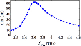
Figure 15. Improvement in conversion efficiency versus frequency of fundamental wave by patterning graphene as a microribbon array for the structure depicted in figure 7 with 
 and
and  and an
  glass substrate instead of an infinite graphene sheet (corresponding to the schematically depicted structures in figures 12(a) and (b) respectively).
Download figure:
Standard image High-resolution imageRegarding the asymmetric behavior of CEI versus the frequency of the FW around the resonant condition in figure 15, one should notice the contribution of the concentration of the electromagnetic field at the ribbon edge in THG. This effect would be much more important in the case of high-intensity illumination at higher frequencies where the difference between an infinite graphene sheet and a ribbon array (sensitivity to the inter-ribbon space) is more distinguishable for the illuminating wave than at lower frequencies (corresponding to longer wavelengths).
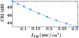
In all of the above simulations, to calculate the amount of enhancement in CE, we have set the intensity of the illuminating wave to be as low as possible (the TH level from the infinite graphene sheet is around −140 dB) such that the red shift in the resonant frequency of the system is negligible and the resonant frequency in the linear case provides a good approximation of the one in the nonlinear case. However, certainly by increasing the illumination intensity, to achieve higher levels of TH, one should be aware that the resonant frequency of the system undergoes a red shift and by working in the resonant frequency obtained from linear simulation, a reduction in THG improvement due to working out of the resonant region may be observed which is demonstrated in figure 16.
Figure 16. The reduction in CEI by increasing the illumination intensity and working in the resonant frequency obtained from the linear simulation for the structure depicted in the inset of figure 12(a) with 

 and an
  glass substrate.
Download figure:
Standard image High-resolution image
All of the results reported in this study are calculated for the transmission mode (according to figures 1 and 7). However, according to our simulations, the results obtained by working in the reflection mode follow the same trend of variation with different parameters consistent with those obtained from the transmission mode and a negligible difference in the order of 2–3 dB in the TH level is observed which may be attributed to the transmission and reflection coefficients of the incident wave at the graphene boundary. Therefore, depending on the experimental facilities or convenience one of these two modes can be employed.
It is worth mentioning that the mechanisms of laser-induced damage to graphene, when illuminated by femtosecond (fs) pulsed lasers compared to CW lasers, are different. With fs pulsed lasers, both thermal and non-thermal effects have a contribution, whereas with CW lasers thermal effects play a dominant role. In terms of peak intensity, graphene can tolerate higher intensities for a shorter pulse at lower average intensity. In total, the reported damage threshold for fs pulsed lasers is  which is much higher than that observed for CW lasers,
  [50, 51, 67–69]. The intensities in our study are much lower than the threshold intensity of graphene damage. Since no loss is taken for the graphene bounding dielectric medium in our simulations, obtaining the same results in an experimental case may be achieved by increasing the intensity of the illuminating wave.
The intensities required for our predicted nonlinear responses can be provided by currently available or recently developed THz lasers [70] such as CO2 lasers or molecular THz lasers (up to  [71], THz lasers with peak electric fields of
  [72], single-cycle THz pulses with electric fields greater than
  [73] and coherent transition radiation sources from relativistic electron bunches with field strength in the order of
  [74].
[74].
6. Conclusion
In this study, we have demonstrated how electromagnetic field enhancement in a graphene microribbon array, under plasmon resonance conditions, can noticeably contribute to the improvement of THG strength, by more than five orders of magnitude based on our FDTD numerical simulations, compared to an infinite graphene sheet. By considering the electric tunability of the graphene first- and third-order conductivities besides the ability of graphene to support the SPP mode at THz frequencies, valuable potential applications for the THz gap region can be developed. We have shown that the resonant frequency of the ribbon array undergoes a blue shift with an increase in graphene Fermi level and period length and a decrease in ribbon width. We have revealed that for a graphene microribbon array of a higher Fermi level and quality (higher carrier mobility and longer relaxation time), a longer period and a narrower ribbon width, a more noticeable improvement in TH level is expected due to the formation of plasmon resonances of higher quality factors. We have explored how the modification of graphene conductivity under intense illumination and the corresponding red shift in the plasmon resonant frequency may lead to a reduction in THG CE in the case of excitation of the system at the resonant frequency obtained from linear simulation, due to working out of the resonance state.