
Abstract
Femtosecond ultrabright cathodes with spatially structured emission are a critical technology for applications such as free-electron lasers, tabletop coherent x-ray sources, and ultrafast imaging. In this work, the optimization of the total electron yield of ultrafast photon-triggered field emission cathodes composed of arrays of nanosharp, high-aspect-ratio, single-crystal silicon pillars is explored through the variation of the emitter pitch and height. Arrays of 6 nm tip radius silicon emitters with emitter densities between 1.2 and 73.9 million tips cm−2 (hexagonally packed arrays with emitter pitch between 1.25 and 10 μm) and emitter height between 2.0 and 8.5 μm were characterized using 35 fs 800 nm laser pulses. Three-photon electron emission for low-energy (<0.3 μJ) light pulses and strong-field emission for high-energy (>1 μJ) light pulses was observed, in agreement with the literature. Of the devices tested, the arrays with emitter pitch equal to 2.5 μm produced the highest total electron yield; arrays with larger emitter pitch suffer area sub-utilization, and in devices with smaller emitter pitch the larger emitter density does not compensate the smaller per-emitter current due to the electric field shadowing that results from the proximity of the adjacent tips. Experimental data and simulations suggest that 2 μm tall emitters achieve practical optimal performance as shorter emitters have visibly smaller field factors due to the proximity of the emitter tip to the substrate, and taller emitters show marginal improvement in the electron yield at the expense of greater fabrication difficulty.
Export citation and abstract BibTeX RIS

Content from this work may be used under the terms of the Creative Commons Attribution 3.0 licence. Any further distribution of this work must maintain attribution to the author(s) and the title of the work, journal citation and DOI.
Introduction
Femtosecond ultrabright cathodes with spatially structured emission are a critical technology for applications such as free-electron lasers, tabletop coherent x-ray sources, and ultrafast imaging [1–3]. State-of-the-art ultrafast cathodes are flat surfaces coated with highly reactive, low-workfunction materials that produce electrons through a single-photon absorption process of ultraviolet light pulses. However, these devices have several disadvantages including (i) they need to be fabricated, stored, and operated in ultra-high vacuum, and (ii) producing high current pulses reduces their lifetime due to the rapid degradation of the low workfunction material [4]. Cathodes based on photon-triggered field emission, i.e., tunneling of electrons due to the interaction of high-intensity optical pulses with field enhancing structures, are a promising technology to bypass these shortcomings [5, 6]. Reported ultrafast photo-triggered field emission cathodes include single-tip sources that are serially manufactured [7–9] and multi-emitter sources that are microfabricated [10–16]. We recently reported batch-fabricated photon-triggered field emission cathodes composed of massively multiplexed (>100 000 tips, 4.6 million tips cm−2), uniform (<1 nm tip radius standard deviation) arrays of nano-sharp high-aspect-ratio silicon pillars [17]; the devices are made using standard CMOS batch fabrication processes, are stored at atmospheric conditions, and can be operated at lower vacuum levels compared to standard photocathodes with no degradation. The devices are capable of pC-level emission with multi-kHz repetition, greatly increasing the total emitted charge per pulse compared to single-emitter sources; in addition, the cathode shapes the emission as a series of electron sheets with periodic transverse structure, which is essential for applications such as x-ray generation through emittance exchange and inverse Compton scattering [18]. In this work, through experiment and simulations, the optimization of the total electron yield of ultrafast photon-triggered field emission cathodes composed of arrays of nanosharp, high-aspect-ratio, single-crystal silicon pillars is explored through the variation of the emitter pitch and height.
Device fabrication
The devices were made from 5 Ω cm, n-type, single-crystal, single-side-polished 150 mm diameter silicon wafers. First, an array of circular features is formed on the wafer using a 250 nm thick low-pressure chemical vapor deposited silicon-rich silicon nitride film, projection optical lithography, and reactive ion etching (RIE). Then, a second array of circular features is created on top of the first array using a 500 nm thick plasma-enhanced chemical vapor deposited silicon dioxide film, projection optical lithography, and RIE; each oxide feature is concentric within 0.1 μm to the nitride feature directly underneath, which is the alignment capability of the projection lithography tool used. Next, the body of the pillars is etched using deep reactive ion etching ; the wafers are then cleaned and oxidized. The oxidation step thins the pillars and the nitride features act as a diffusion barrier to form the tips with low tip diameter spread. The oxide and nitride films are removed using wet etchants, resulting in highly uniform hexagonally packed arrays of single-crystal silicon pillars, each topped by an ultrasharp tip. We fabricated arrays of silicon emitters with 6 nm tip radius and emitter height equal to 2, 4, and 8.5 μm, hexagonally packed with emitter pitch equal to 1.25, 2.5, 5, and 10 μm (1.2–73.9 million emitters cm−2). The shape of the silicon emitters resembles a cone with a sidewall inclination of 2.4° with respect to the normal of the substrate. Figure 1(a) shows a schematic of the fabrication process flow, and figure 1(b) shows an SEM of the cross-section of a fabricated array of high-aspect-ratio nanosharp Si pillars with a close-up of one of the emitter tips. Right before characterization, the chip was dipped in 2% HF acid to remove the native oxide.

Figure 1. Fabrication process flow schematic (a); SEM cross-section view of an array of high-aspect-ratio Si pillars with 1.25 μm pitch, 8.5 μm height and tip radius of 6 nm (b).
Download figure:
Standard image High-resolution imageExperimental procedure
Characterization of the devices in a diode configuration was conducted inside a vacuum chamber with pressure below 5 × 10⁻⁸ Torr. The chip was connected to ground through a picoammeter (Keithley 6485), while the anode electrode, i.e., a 0.25'' diameter plate placed 3 mm above the chip, was connected to a source-measuring unit that provided bias voltages between 10 and 5000 V (Keithley 237 for 10–1000 V, and Keithley 248 for 1000–5000 V). The cathode was excited with 35 fs 800 nm laser pulses at 3 kHz repetition rate from a regeneratively amplified titanium sapphire oscillator seed. The laser pulses illuminated the samples at an 84° grazing incidence, which defined a roughly 765 μm by 80 μm ellipsoidal spot on the substrate. The energy of the incident pulses was controlled using a half-waveplate and polarizer together with various neutral density filters (0, 10 and 20 db). The polarization angle was optimized to align the K vector with the axis of the emitters and the pulse compression of the laser was tuned to maximize the current emitted per pulse. Each sample was actuated for at least 20 min using 1.4 μJ pulses while the anode is biased at 100 V to remove any absorbed gases from the tips and stabilize the emission. The anode bias voltage was swept between 10 and 5000 V; at each anode bias voltage, the energy of the incident laser pulses was varied between 0.04 and 10 μJ. The average emitter and anode currents were recorded for each combination of anode bias voltage and laser pulse energy. It was verified that in each data point the emitted and collected currents were the same. The current was then converted to emitted charge per pulse by dividing the average current value by the repetition rate of the laser.
Results and discussions
Figure 2 shows the total emitted charge per pulse versus incident laser pulse energy from arrays with emitter pitch equal to 1.25, 2.5, 5, and 10 μm, and emitter height equal to 2, 4, and 8.5 μm; in these experiments the anode bias voltage was set at 1000 V. Each charge-incident photon pulse energy characteristic has three distinctive regimes: a multi-photon regime for low-energy pulses (<0.3 μJ), a field emission regime for high-energy pulses (>1.0 μJ), and a transition regime between the multi-photon and field emission regimes (i.e., the kink in each characteristic). At low laser pulse energy (<0.3 μJ), each emitted electron absorbs three photons in order to escape from the tip surface because the electron affinity of Si is 4.05 eV and the energy of the photons at 800 nm used in the experiments is 1.55 eV. Furthermore, the power dependence slopes of the low-intensity portion of the charge-pulse energy characteristics are about 3, in agreement with a three-photon absorption process [19].

Figure 2. Total emitted charge per pulse versus incident laser pulse energy for arrays of emitters with height equal to 2, 4, and 8.5 μm and pitch equal to (a) 1.25 μm, (b) 2.5 μm, (c) 5 μm and (d) 10 μm. In these measurements the anode bias was set at 1000 V. In each plot the power dependence slopes for the high-energy portions of the curves are shown, as well as reference cubic power dependence lines next to the low-energy portions of the curves (P is the incident energy).
Download figure:
Standard image High-resolution imageAt high laser pulse energies (>1.0 μJ), electrons tunnel into the continuum faster than an optical period [20, 21]; this regime is commonly referred to as the strong-field or tunneling regime and it follows a time-averaged Fowler–Nordheim model [22]. The strong-field emission model without space charge effects presented in [17] predicts that the slope at the highest current yield is 1.2 at a fixed bias of 1000 V; the high-energy slopes in figures 2(c) and (d) are close to this value, but the high-energy slopes of figures 2(a) and (b) are not. This can be explained by the development of a space charge-induced virtual cathode at smaller pitches; as electrons form a current sheet above the emitter, this virtual cathode suppresses the electron emission [23]. The strong field emission model with space–charge effects presented in [17] predicts a slope of 0.51 at the highest current yield with a bias of 1000 V—in close agreement with the high-energy slopes of figures 2(a) and (b). In figure 2(d), corresponding to the data with emitter pitch equal to 10 μm (i.e., the largest emitter pitch investigated), the total charge emitted per pulse augments with increasing emitter height, although the charge versus laser pulse energy characteristics converge for an incident laser pulse energy >1 μJ for devices with emitter height >4 μm. In figures 2(a)–(c) the charge versus pulse energy characteristics almost overlap, regardless of the emitter height. Therefore, the data suggest that the effect of the pillar height in the charge versus pulse energy characteristic greatly diminishes for decreasing emitter pitch.
The total charge versus incident photon energy data with anode bias voltage set at 1000 V are shown in figure 3, grouped this time by the emitter height instead of the emitter pitch. In all cases, for a fixed emitter height, the total charge emission per pulse increases with decreasing emitter pitch, down to 2.5 μm; further reduction of the emitter pitch results in less charge emission. The total emission of the array depends on the number of emitters and the current per emitter. There is a trade-off between the field enhancement attained by the emitters and the number of emitters as the emitter pitch is scaled down. As the emitter pitch is reduced, the field enhancement of the emitters is also reduced because of electric field shadowing from the adjacent emitters. There is an exponential dependence of the field emitted current on the field factor, while the number of emitters per unit of area geometrically increases as the emitter pitch is reduced. Down to 2.5 μm emitter pitch, the result of the trade-off is a net gain in the total current production; smaller emitter pitch results in a net loss of the total current emission. Of the devices tested, the arrays with emitter pitch equal to 2.5 μm produced the highest total charge emission; however, it does not necessarily imply that 2.5 μm is the optimum pitch since the pitch was varied across a range using a few discretized values. The data shown in figure 3 suggest that in all cases the charge versus incident laser pulse energy characteristics converge into a space–charge limit characteristic at high pulse energy; however, the convergence seems to take place for intensities beyond 10 μJ, which is close to the damage threshold energy for silicon photo-triggered field emission arrays (∼20 μJ) [17]. Similar behavior of the charge versus incident laser pulse energy characteristics was obtained when conducting the experiments with an anode bias voltage of 100 V, shown in figure 4, although the electron yield is smaller.

Figure 3. Total emitted charge per pulse versus incident laser pulse energy for emitter arrays with emitter pitch equal to 1.25, 2.5, 5 and 10 μm, and emitter height equal to (a) 2 μm, (b) 4 μm, and (c) 8.5 μm. In these experiments the anode bias voltage was set at 1000 V.
Download figure:
Standard image High-resolution image
Figure 4. Total emitted charge per pulse versus incident laser pulse energy for emitter arrays with emitter pitch equal to 1.25, 2.5, 5 and 10 μm, and emitter height equal to (a) 2 μm, (b) 4 μm, and (c) 8.5 μm. In these experiments the anode bias voltage was set at 100 V.
Download figure:
Standard image High-resolution imageThe emitted charge per tip per pulse as a function of the emitter pitch was also investigated. The emission per tip was estimated assuming uniform operation of the array, dividing the total emission by the number of emitters within the laser spot size (a roughly 765 μm by 80 μm ellipse). Figure 5 shows that a larger emitter pitch implies better emission per emitter at high laser pulse intensities (>2 μJ) due to the better field enhancement of the tip as there is more space between emitters, and the appearance of space charge effects in the arrays with smaller pitch as evidenced by the high-energy slopes of the characteristics shown in figure 2. The emission per emitter of the arrays with 2.5 μm emitter pitch is lower than that of the arrays with larger emitter pitch, evidencing reduced enhancement due to the proximity effect of the tips.

Figure 5. Emitted charge per emitter per pulse versus incident laser pulse energy for arrays of emitters with emitter pitch equal to 1.25, 2.5, 5 and 10 μm, and emitter height equal to (a) 2 μm, (b) 4 μm, and (c) 8.5 μm. In these experiments the anode bias voltage was set at 1000 V.
Download figure:
Standard image High-resolution imageThe variation of the total charge emission as a function of the anode bias voltage was also explored. Figure 6 shows the charge versus anode bias voltage for devices with emitter height equal to 8.5 μm when the laser pulse energy is set at 8.4 μJ. The device with 2.5 μm emitter pitch has the highest emission at all bias voltages. The power dependence slopes in all characteristics are similar (∼0.28) and close to the slope found in [17] (∼0.33). The voltage dependence slope is smaller than 1, indicating that the emission is limited by the space charge due to the virtual cathode effect.

Figure 6. Total emitted charge per pulse versus anode bias voltage at an incident laser pulse energy equal to 8.4 μJ for arrays of emitters with emitter height equal to 8.5 μm and emitter pitch equal to 1.25, 2.5, 5 and 10 μm.
Download figure:
Standard image High-resolution imageFigure 7 shows the computed quantum efficiency (QE), i.e., the number of electrons emitted per incident photon, for the total emitted charge per pulse versus incident photon energy when the anode bias voltage is equal to 1000 V. In figures 7(a)–(c), QE first increases rapidly at low energies (<0.6 μJ), corresponding to the three-photon absorption regime and the transition regime between multi-photon and strong-field regimes; at high energies (>1 μJ), which corresponds to the strong-field emission regime, QE saturates and becomes flat. For the emitter pitch values of 1.25 and 2.5 μm, QE reaches a maximum around 0.4 μJ, to then bend down, presumably due to the virtual cathode effect. The maximum estimated QE is equal to 8.2 × 10⁻⁷ and corresponds to the array with emitter height equal to 4 μm and emitter pitch equal to 2.5 μm. However, the QE versus incident photon energy characteristics for all devices with emitter pitch equal to 2.5 μm are fairly similar, as shown in figure 7(d). The QE values obtained are high considering that only a very small fraction of the array surface is utilized, as the tip diameter is ∼12 nm and the tip spacing is on the order of microns. The QE of planar Si is 10−10 [17].

Figure 7. Quantum efficiency as a function of incident laser pulse energy for devices with emitter pitch equal to 1.25, 2.5, 5, and 10 μm and emitter height equal to (a) 2 μm, (b) 4 μm, and (c) 8.5 μm; (d) summary of quantum efficiency characteristics for devices with 2.5 μm emitter pitch.
Download figure:
Standard image High-resolution imageData were collected to examine the emission stability of the cathode technology using a array with emitter height equal to 8.5 μm and emitter pitch equal to 2.5 μm; in these experiments four different combinations of incident energy and anode bias voltage were used while continuing operating the device for 1800 s. The current emitted is plotted as a function of time in figure 8. All four curves show stable current emission after over 5 million pulses and no signs of deterioration are observed. The lowest constant current emission has the lowest noise compared to the others because small perturbations in the electric field (i.e. the laser intensity) result in large changes to the emitted current (this is why the emitter current is usually plotted in log scale; in figure 8 it is plotted in linear scale for clarity). The highest emitted current shows an average 2.4 pC per pulse emission (7.2 nA of average current) at the incident energy of 9.5 μJ and anode bias voltage of 5000 V.

Figure 8. Total emitted charge per pulse for a given incident photon pulse energy and anode bias voltage as a function of time for an emitter array with emitter height equal to 8.5 μm and emitter pitch equal to 2.5 μm.
Download figure:
Standard image High-resolution imageThe dependence of the geometry of the emitter (height) and emitter array (pitch) in the field enhancement of the emitter was investigated using finite element models with Floquet periodicity and the frequency domain analysis module of the commercial software COMSOL Multiphysics. We used the materials library of the software to assign the physical properties of the emitter material. The Fowler–Nordheim equation relates the field-emitted current to the electrostatic field at the surface as [24]

where I is the current from the tip, αtip is the emission area, AFN and BFN are constants, F is the maximum normal electric field on the surface of the emitter tip, and t(y) and v(y) are Nordheim elliptic functions. The maximum normal electric field on the surface of the emitter tip is enhanced by the emitter tip from the electric field of the incident photons and can be expressed as

where  is the dimensionless field factor of the tip (a measure of the field enhancement of the tip), and
  is the electric field of the incident photons.
We validated the simulation framework by verifying the Fresnel equations between Si and vacuum before inserting the Si pillar. The Fresnel equations describe the behavior of light when moving between media with different refractive indices. Equation (3) predicts the p-polarized reflectance, Rp, between two media when a pulse traveling in medium 1 reflects on medium 2:
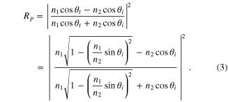
In our case n1 is the refractive index of vacuum and n2 is the refractive index of Si, θi is the incident angle (84°), and θt is the refractive angle from Snell's law. The code yielded results similar to the prediction of equation (3) within 3%.
We originally implemented 3D models of the array unit cells but we found that the simulations did not converge for emitter pitch above 1.75 μm and emitter height above 2 μm; we believe this was due to the large number of finite elements in the simulations and the memory capabilities of our simulation platform, as finite elements with side as small as 1.5 nm were required to accurately map the geometries and the spatial transitions of the solution. Therefore, we implemented 2D simulations of the arrays instead. The field factor predicted by the 2D simulation and the field factor predicted by the 3D simulation do not agree. For example, the 3D simulation of the case where the emitter pitch is equal to 1 μm and emitter height equal to 2 μm predicts a field factor equal to 4.2, while the corresponding 2D simulation predicts a field factor equal to 1.7. This is not surprising because a 3D model describes a planar array of tapered tips while a 2D model describes a linear array of tapered ridges, and 3D features concentrate the field lines more effectively than 2D features, resulting in higher field factors. However, the results of the 2D simulations reveal trends that qualitatively resemble the behavior of the 3D case.
First, arrays with emitter height equal to 2 μm, emitter pitch in the 1–100 μm range in 0.1 μm steps, and tip radii equal to 6, 12, and 24 nm were simulated (i.e., a total of 2973 independent simulations); the results are shown in figure 9. In general, the field factor increases for increasing emitter pitch, to eventually reach a limit value; however, we observe oscillations of the field factor that are more pronounced for small values of emitter pitch. A fit proportional to  where r is the tip radius and n = 0.278, closely describes the asymptotic values of the field factor obtained in the simulations. Finer discretization of the emitter pitch range using photons with wavelength equal to 800, 900, 1000, and 2000 nm revealed that the oscillations of the field factor are periodic with separation between adjacent peaks a little over half the wavelength of the photons (0.517). The ripples in the field factor can be explained by Bragg diffraction [25], where the distance p between consecutive peaks is given by

where λ is the wavelength of the photons and θ is the incident angle. Given that the emitter arrays have hexagonal packing, we speculate that the period of the ripples would be different for different directions of propagation of the incident laser pulse with respect to the orientation of the array. However, we could not verify this hypothesis because of the convergence problems we had with the 3D simulations.

Figure 9. Simulated emitter field factor versus emitter pitch for 2 μm tall emitters with emitter tip radii equal to 6, 12, and 24 nm.
Download figure:
Standard image High-resolution imageSimulations of the emitter field factor for varying emitter height between 0.4 and 2 μm were also conducted. In this case, the emitter height was varied in steps of 0.4 μm while the emitter pitch was varied in the 1–100 μm range in steps of 0.1 μm (i.e., a total of 4955 independent simulations); the result is shown in figure 10. A similar trend to the curves shown in figure 9 is observed, i.e., the field factor increases rapidly to then saturate as the emitter height is increased and a periodic oscillation with separation between adjacent peaks equal to 51.7% the wavelength of the photons. Also, it is clear that the field factor increases with the height of the pillar, up to a point where further increase yields minimal differential returns. This is an important result because making devices with larger emitter height is harder and more expensive, and the extra complexity would be unjustified given the results obtained. For example, the results of this work suggest that the emitters in [17] are unnecessarily long by a factor of 20 to achieve roughly the same emission characteristics.

Figure 10. Simulated emitter field factor versus emitter pitch for 6 nm tip radius emitters with emitter height equal to 0.4, 0.8, 1.2, 1.6, and 2.0 μm.
Download figure:
Standard image High-resolution image
Conclusion
The emission of electrons from planar arrays of photon-actuated, high-aspect-ratio, single-crystal silicon nanosharp electron emitters that span a range of emitter height and pitch was investigated using ultrashort photon pulses. Arrays of 6 nm tip radius silicon emitters with emitter densities between 1.2 and 73.9 million tips cm−2 (i.e., emitter pitch between 1.25 and 10 μm) and emitter height between 2.0 and 8.5 μm were characterized using 35 fs 800 nm light pulses. For low-energy incident photon pulses (<0.3 μJ) the data are consistent with a three-photon absorption process, while for high-energy incident laser pulses (>1 μJ) the data are described by a time average Fowler–Nordheim model strong-field emission, in agreement with the literature and the models. Of the devices tested the arrays with emitter pitch equal to 2.5 μm produced the highest total electron yield, while 2 μm tall emitters achieve practical optimal performance, as taller emitters only show marginal improvement in the electron yield at the expense of a more difficult fabrication process.
Acknowledgments
The devices were fabricated at the Microsystems Technology Laboratories, MIT. This work was funded by the Defense Advanced Research Projects Agency/Microsystems Technology Office (DARPA/MTO) under contract N66001-11-1-4192 (program manager D Palmer). Any opinions, findings, and conclusions or recommendations expressed in this publication are those of the authors and do not necessarily reflect the views of the US Government and therefore, no official endorsement of the US Government should be inferred.