
Abstract
Current–voltage and Kelvin probe force microscopy (KPFM) measurements were performed on single ZnO nanowires. Measurements are shown to be strongly correlated with the contact behavior, either Ohmic or diode-like. The ZnO nanowires were obtained by metallo-organic chemical vapor deposition (MOCVD) and contacted using electronic-beam lithography. Depending on the contact geometry, good quality Ohmic contacts (linear I–V behavior) or non-linear (diode-like) contacts were obtained. Current–voltage and KPFM measurements on both types of contacted ZnO nanowires were performed in order to investigate their behavior. A clear correlation could be established between the I–V curve, the electrical potential profile along the device and the nanowire geometry. Some arguments supporting this behavior are given based on technological issues and on depletion region extension. This work will help to better understand the electrical behavior of Ohmic contacts on single ZnO nanowires, for future applications in nanoscale field-effect transistors and nano-photodetectors.
Export citation and abstract BibTeX RIS
1. Introduction
As low dimensionality and high surface to volume ratio have a major impact on overall photodetection performance, there has been an increased interest in recent years in the use of semiconductor nanowires as photodetectors. A wide variety of semiconductor materials have been used, such as Si [1], GaN [2], GaAs [3], ZnO [4–7], Ge [8, 9], ZnTe [10], CdS [11], SnO2 [12], InN [13] and W18O49 [14]. Some of the reported results prove that single nanowires can actually exhibit strong photoconduction gain. Among them, ZnO nanowires have been of particular interest as photoconduction gains as high as 1010 [7] in the UV region were reported. Such a high gain means that the photon–electron conversion can reach several orders of magnitude in a single nanowire which can be sufficient to detect single photons or at least to detect very low intensity light. ZnO nanowires seem thus ideal for applications requiring high spatial resolution (sub-micron resolution) and low optical power detection such as single molecule applications for biology or for quantum optics experiments.
Nevertheless, several issues come into play when it comes to making a precise measurement of the photoconductive gain of a single nanowire. An important issue is the good quality of the injecting contacts on the nanowire and the reproducibility of its characteristics. Current–voltage (I–V) measurements of biased nanowires [15] and local surface potential mapping using KPFM [16–26] are generally used in order to characterize the contacted nanowires. In this paper, we present the electrical characterization results of ZnO nanowires obtained by MOCVD and contacted by Ti/Au pads using e-beam lithography [27].
2. Experimental details
The ZnO nanowires are epitaxially grown on A-plane sapphire substrates by metalorganic chemical vapor deposition in a horizontal reactor operating at a reduced pressure of 65 mbar. The substrate holder (graphite covered with SiC) can be heated up to 1000 ° C using RF induction. The reactor walls are not cooled. Diethylzinc (DEZn) and nitrous oxide (N2O) with partial pressures of 9.1×10⁻³ mbar and 8.6 mbar were respectively used as zinc and oxygen sources. The carrier gas was helium. The ZnO nanostructures, consisting of nanowires emerging on the top of hexagonal pyramids, were grown at a temperature of 875 ° C using an oxygen/zinc molar ratio of 940, in order to ensure the formation of vertically aligned nanowires with high aspect ratio. The densely packed vertical ZnO nanowires were then sonicated in an ethanol solution in order to remove them from the initial substrate. Single nanowires are obtained by drop-casting the resulting solution on a silicon substrate with a top SiO2 insulating layer of 400 nm (estimated by ellipsometry measurements). Electrical contacts on single nanowires were obtained using a lift-off technique based on e-beam lithography on PMMA resist. Using a mechanical indenter, an alignment grid is drawn on the surface to perform the lithography in a single step. More details on the fabrication process can be found in [27]. The photoluminescence spectra of single nanowires are first measured using a microphotoluminescence setup in order to select good quality ZnO nanowires. The selected ones were the ones presenting high photoluminescence intensity and good waveguiding effect along the nanowire, thus ensuring a fairly good structural NW. The indenter marks are then used as alignment marks for the e-beam lithography which will define the contact pads for the nanostructures (figure 1(b)). We finally evaporated 30 nm of titanium and 300 nm of gold on the substrate followed by the lift-off procedure.
The contacted nanowires were characterized using current–voltage and surface potential measurements (figure 1). The electrical characterizations were performed using an Agilent 5270B analyzer and were done in the dark to avoid any spurious effect due to the light environment. The surface potential measurements on biased ZnO nanowires have been performed using the Kelvin probe force microscopy technique (KPFM) [28, 29]. For that, a Dimension 3100 atomic force microscope (AFM) was used in the lift mode. All AFM measurements have been performed in a clean room environment with a constant temperature of 21 ° C and a relative humidity of 30%. The AFM/KPFM setup is placed into a glove box where the relative humidity can be decreased down to about 5% through a closed-loop air drying system. Conductive tips coated with Pt/Ir with a resonant frequency of around 75 kHz were used. The measurement method consists of two consecutive probe scans for each raster scan line: the first scan measures the topography of the sample whereas the second scan measures the local potential using the Kelvin probe technique [30].

Figure 1. Experimental setup for ZnO nanowire characterization: AFM and probe-station image (left) and cross-section schematics of the electrical connections (right).
Download figure:
Standard image High-resolution imageThe surface potential distribution is measured using the 'Kelvin probe' method [28, 29]. To overcome the influence of the surface topography in the potential measurements each AFM scan line is imaged in two steps (lift mode): firstly the tip follows the surface topography which is recorded (Step 1), then it is removed from the surface and placed at a distance of about 100 nm (Step 2). Following the previously recorded topographic profile, the tip hovers over the scan line at a constant height and performs the potential measurement, thus eliminating eventual artifacts arising from the sample surface topography.
During this measurement (Step 2) the feedback is no longer provided in z as the tip follows the prerecorded topography profile. Instead, a voltage is applied on the conductive cantilever which is composed of an AC component Vacsin(ωt) and a DC voltage Vdc. The AC component is used to actuate the cantilever and the DC voltage is applied to compensate the electrostatic force component Fω experienced by the probe tip at the excitation frequency.
In the case of a metallic sample surface, if a voltage is applied on the cantilever (with the sample grounded), the energy U of the cantilever-surface capacitive system is expressed by

where Δφ is the workfunction difference between the cantilever and the sample surface and Vdc, Vac the DC and AC components of the applied voltage on the cantilever. The cantilever-surface capacitive force in lift mode (Step 2) is expressed by

where


As can be seen from equation (4) the surface potential Δφ can be determined by applying a Vdc voltage on the cantilever so that the Fω component of the total force be brought to zero (Vdc =− Δφ for Fω = 0). Therefore the feedback in lift mode is no longer in z (the tip is following the prerecorded topography profile measured in Step 1) but on Vdc with a zero set-point for the Fω component.
In the case of imaging the surface potential generated by charges present in a biased device, the tip–sample interaction force acting on the tip during lift mode is dependent on the lift height (z) [29, 31]. The lift height can therefore be chosen according to the level of lateral resolution required for the KPFM measurement. The tip height was set to 100 nm during all KPFM measurements presented in this work.
3. Results and discussion
ZnO nanowires with diameters between 120 and 250 nm and length between 11 and 16 μm were measured (as shown in figure 2).

Figure 2. AFM 3D image of a contacted ZnO nanowire (left) with a corresponding cross-section (right) showing an average nanowire width of 130 nm.
Download figure:
Standard image High-resolution imageAs depicted in figure 3 most nanowires exhibit linear I–V behavior, showing that the technological process provides good Ohmic contacts.

Figure 3. SEM image (left) and current–voltage measurement (right) of a ZnO nanowire showing linear (Ohmic) behavior.
Download figure:
Standard image High-resolution imageSurface potential maps of the linear nanowire were obtained using the KPFM technique for different bias voltages. Figure 4 presents the KPFM measurements for a 1 V bias applied in a forward (figure 4(a)) and reverse (figure 4(b)) direction. As can be observed in the longitudinal potential cross-section graph (figure 5), the potential distribution along the ZnO nanowire with linear contacts is identical regardless of the bias voltage application direction, as expected from Ohmic contacts. Also a linear potential profile is clearly observed along the whole nanowire between the contacts. From the I–V measurements, neglecting the Ohmic contact series resistances contributions, the nanowire resistivities are estimated to be between 0.20 and 1.9 Ω cm (with resistances ranging from 0.25 to 2.4 MΩ), for an electrode spacing of 4 μm and an average nanowire diameter of 200 nm [27]. Upon applying a gate voltage (between +10 and −10 V, not shown here), we found that the ZnO NWs were n-doped, which is in good agreement with standard residual doping in ZnO [32]. From a two-probe I–V measurement the contact contribution cannot be distinguished from the nanowire intrinsic resistance. However, the estimated resistivities are in good agreement with approximated values calculated considering a residual doping density in the range 1016–1017 cm−3 and a drift mobility of 100 cm2 V−1 s−1, typical values for ZnO [32].
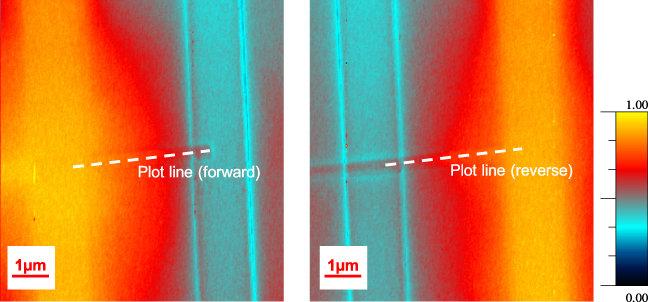
Figure 4. Potential measurements on a contacted ZnO nanowire with linear I–V behavior for a forward (left) and reverse (right) bias (U = 1 V). A symmetric behavior is observed. Color scale varies from 0 to 1 V.
Download figure:
Standard image High-resolution image
Figure 5. Measured topography and electrical potential variation along a ZnO nanowire with Ohmic contacts.
Download figure:
Standard image High-resolution imageA diode-like I–V behavior was also found for a small fraction of the contacted nanowires (figure 6) due to the presence of one Schottky-behaving Au–ZnO contact.

Figure 6. SEM image (left) and I–V measurement (right) on a non-Ohmic ZnO nanowire.
Download figure:
Standard image High-resolution imageThe surface potential of such Schottky-behaving contacts was also investigated using KPFM measurements. Figure 7 presents the generated surface potential distributions for forward (figure 7(a)) and reverse (figure 7(b)) bias. As can be seen from the longitudinal cross-section along the nanowire (figure 8), the potential profile is linear for the forward bias (similar to figure 5) and highly non-linear for reverse bias. Figure 9 represents a schematic band diagram of a Schottky contact. From this picture, one can see that when a forward bias is applied, the voltage drop in the depletion region of the Schottky contact is very limited: the applied bias is then quasi-linearly distributed over the whole nanowire length. In contrast, under reverse bias, the depletion region at the Schottky contact extends into the ZnO volume, and most of the applied voltage is lost at this region. Consequently, the measurement shows an almost constant potential distribution along the nanowire, but a sharp voltage drop at the ZnO nanowire Schottky contact vicinity. This situation is illustrated in figure 9 (right).
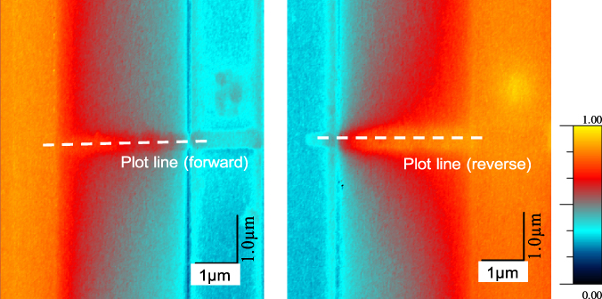
Figure 7. Potential measurements on a contacted ZnO nanowire with diode-like I–V behavior for a forward (left) and reverse (right) bias (U = 1 V). Color scale varies from 0 to 1 V.
Download figure:
Standard image High-resolution image
Figure 8. Measured topography and electrical potential variation along a ZnO nanowire with a Schottky contact.
Download figure:
Standard image High-resolution image
Figure 9. Schematic band diagram of a Schottky contact under forward (left) and reverse (right) bias. ΦB is the barrier height at the metal–semiconductor contact, EFm and EFS are respectively the Fermi level in the metal and in the semiconductor. The gray areas represent the extensions of the depleted region at the metal/semiconductor interface.
Download figure:
Standard image High-resolution image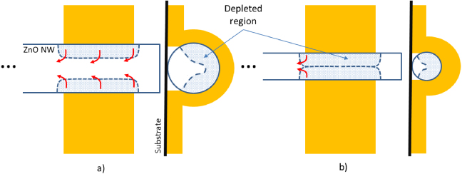
Figure 10. Schematic top and side views of thick (a) and thin (b) ZnO nanowires and their gold contacts under reverse bias, illustrating the effect of the depleted region extension. The schematic arrows indicate current flow under the partially or fully depleted contacts.
Download figure:
Standard image High-resolution image
A possible explanation for the Ohmic or diode-like contact behavior follows observation of the nanowire shape. Due to the growth conditions, all the nanowires are slightly needle shaped. From a quantitative head and tail diameter study using an electron-beam microscope, it turned out that the head to tail diameter ratio of the nanowires are above 70% for all the Ohmic behaving contacts, and decreases to between 50 and 70% for the Schottky-behaving contacts. In fact, the Schottky-behaving contact was always located at the narrow side of the wire. Some fabrication issues cannot be discarded due to the very thin needle end of these nanowires, such as lithography, metal deposition, or very limited contact surface between the metal and the ZnO.
Another phenomenon may emphasize the non-linear behavior in narrow wires, if one considers a residual depletion region being present at the contact/ZnO interface, as illustrated figures 9 and 10. On thin tail devices, the nanowire diameter under the contact may be lower than the depletion region extension. In this case the nanowire may become fully depleted under the contact, and may become highly resistive (figure 10(b)), generating a non-linear I–V behavior. More precisely, considering a junction with a barrier ranging from 0.05 to 0.1 eV, a residual doping density of 1017 cm−3, and an applied bias in the range 0–1 V, the depletion region could extend over 20–100 nm (following usual junction depletion length calculation [33]). Depending on the wire diameter below the contact, the nanowire could be either conductive or highly resistive.
4. Conclusions
Current–voltage characterization and Kelvin probe potential mapping were performed on single nanowire devices made of ZnO, showing a good Ohmic I–V behavior correlated to a linear distribution of the electric potential along the nanowire. Some Schottky-behaving nanowire devices were also identified and characterized. In this case, KPFM potential measurements revealed an abrupt potential drop at the Schottky contact vicinity, as expected from the presence of a depletion region in such contacts. This behavior could be correlated to the needle shape of the nanowires, and in particular a diode-like I–V curve is observed for nanowires exhibiting one very narrow end. Non-linear I–V behavior observed in very narrow nanowires is thought to be enhanced due to a depleted zone extending over the entire ZnO volume under the contact.
Acknowledgments
We acknowledge the help of B Guelorget from LASMIS for the use of the micro-indenter. The authors would like to thank the Champagne-Ardenne region for supporting this work via the 'NanoGain' project. All the fabrication and some of the characterization of this work was realized using the Champagne-Ardenne region platform 'Nanomat' funded by the DRRT Champagne-Ardenne and the European FEDER program. We also want to acknowledge the partial support of the 'Labex ACTION' program (contract ANR-11-LABX-01-01).