
Abstract
We have investigated the growth of self-catalyzed GaAs/GaAsxSb1−x core–shell nanowires directly on Si(111) substrates by molecular beam epitaxy. The compositions of the GaAsxSb1−x shells are tuned in a wide range where the Sb-content is varied from 10 to ∼70%, covering the miscibility gap. In addition, the GaAsxSb1−x shells are grown on both zinc blende (ZB) and wurtzite (WZ) crystal structures. Morphological and structural characterizations of the grown nanowires indicate successful transfer of the GaAs core crystal structure to the GaAsxSb1−x shells for both ZB and WZ nanowires, with slower shell growth rate on the WZ segments.
Export citation and abstract BibTeX RIS
1. Introduction
The growth of axial and radial heterostructure nanowires allows combination of various materials with interesting properties for both fundamental material science studies and a variety of device applications. GaAs/GaAsxSb1−x is one of the promising material combinations, due to the tunable GaAsxSb1−x wavelength covering the important telecommunication spectrum and their type-II band alignment suitable for numerous device applications, especially for solar cells [1, 2]. So far, there have been several reports on the axial heterostructural growth of both Au-free and Au-assisted GaAs/GaAsxSb1−x nanowires by molecular beam epitaxy (MBE) [2–5]. Furthermore, photoluminescence (PL) properties of these nanowires and their significant dependence on the crystal structures have been extensively studied [6]. All the above mentioned studies report that GaAsxSb1−x inserts always adopt zinc blende (ZB) crystal structure and even by adding Sb flux to GaAs nanowires with wurtzite (WZ) crystal structure, the crystal structure instantly changes to ZB. In fact, a literature review on Sb-based nanowires indicates that they almost always prefer to grow in ZB crystal structure, partly related to their low ionicity [7]. Despite the advances made in the growth of axial heterostructure GaAs/GaAsxSb1−x nanowires, the radial heterostructural growth of these nanowires has not been fully investigated. Therefore, employing the core–shell geometry offers a simple way to explore the WZ crystal structure of the GaAsxSb1−x shells. In addition, GaAsxSb1−x is known to have a large miscibility gap [8] which restricts the compositional tuning of this material. It should be mentioned that there are several bulk growth studies demonstrating that metastable GaAsxSb1−x layers within the miscibility gap could be grown on the lattice matched substrates such as InP by using low V/III ratio and low temperatures [9–11].
We report on the successful growth of self-catalyzed GaAs/GaAsxSb1−x core–shell nanowires directly on the Si(111) substrates by MBE. The main significance of the self-catalyzed growth approach is to avoid introducing any external material within the system such as Au and also to prevent unwanted axial GaAsxSb1−x growth during the shell growth. The compositions of the GaAsxSb1−x shells were tuned and the Sb-content was varied in the range of 10 to ∼70%, covering the miscibility gap. In addition, we have investigated the growth of GaAs/GaAsxSb1−x nanowires in both ZB and WZ crystal structures, demonstrating that the core–shell geometry enables transfer of the GaAs structure to the GaAsxSb1−x shells.
2. Experimental details
All the growths were performed in a Varian Gen II Modular MBE system. Solid state Ga source together with As and Sb valved crackers were employed. The use of crackers allows for adjustment of the proportion of dimers and tetramers. The nanowires were grown by using As tetramers and Sb dimers. P-type Si(111) wafers were used as substrates.
The GaAsxSb1−x shells were grown on both ZB and WZ GaAs core nanowires. The WZ GaAs core nanowires were grown by inserting a short GaAsSb segment after the ZB GaAs core nanowire, followed by the GaAs nanowire growth (GaAs/GaAsSb/GaAs) which allows formation of the WZ GaAs nanowires [5]. All the GaAs core nanowires studied in this work (both the WZ and ZB crystal structures) were grown at 640 ° C with planar equivalent GaAs growth rate of 0.7 ML s−1 on GaAs(100) substrate and As flux with beam equivalent pressure of 5.6 × 10⁻⁶ Torr. In order to grow GaAsxSb1−x shell around the core GaAs nanowires and to avoid axial GaAsxSb1−x growth, after the core growth, Ga droplets were solidified under only high As flux of 1.3 × 10⁻⁵ Torr for 10 min. In case of ZB GaAs core nanowires, the solidification process was performed at the same temperature as the core nanowire growth (640 ° C). For the GaAs/GaAsSb/GaAs core nanowires, a lower solidification temperature of 550 ° C together with Sb flux of 1.15 × 10⁻⁶ Torr were supplied during the solidification time (10 min) to avoid GaAsSb insert decomposition and kinking issue. The GaAsxSb1−x shell growth was done by using the same Ga and As fluxes as the core nanowires and adding various Sb fluxes from 1.6 × 10⁻⁶ to 2 × 10⁻⁷ Torr.
After the growth, nanowires were morphologically characterized in a Zeiss Ultra field emission scanning electron microscope (FE-SEM). High resolution transmission electron microscopy (HRTEM) was used to determine the crystal structure of the grown samples (TEM-JEOL 3000F operated at 300 kV). For the TEM characterization, nanowires were broken off from the substrate and transferred onto carbon-coated Cu grids. Additionally, high angle annular dark field scanning transmission electron microscopy (HAADF STEM) and x-ray energy dispersive spectroscopy (XEDS) were used to determine the chemical composition of the obtained nanowires together with the shell thickness.
3. Results and discussion
Figure 1(a) shows a schematic illustration of a Ga-assisted GaAs core nanowire grown directly on the Si(111) substrate, which similar to the Au-assisted growth proceeds via a vapor–liquid–solid (VLS) growth mechanism. A SEM micrograph of such a Ga-assisted GaAs nanowire is shown in figure 1(c). As mentioned in section 2, after the growth of GaAs core nanowires, the Ga droplets on top of the nanowires were solidified, and then the GaAsxSb1−x shells were grown in a vapor–solid growth mechanism [12]. Figure 1(b) schematically illustrates a GaAs/GaAsxSb1−x core–shell nanowire with prismatic hexagonal tip shape, and figure 1(d) shows a SEM image of such a grown nanowire. Figures 1(e) and (f) show top and side cross sectional schematic views of GaAs/GaAsxSb1−x core–shell nanowires, respectively.
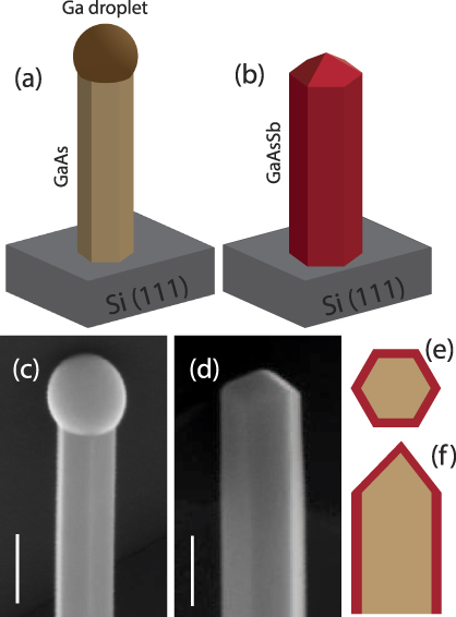
Figure 1. Schematic illustration of (a) a self-catalyzed GaAs core nanowire directly grown on Si(111) substrates. (b) A GaAs/GaAsxSb1−x core–shell nanowire where GaAsxSb1−x shell is grown after the Ga-solidification process. Magnified SEM images of (c) a self-catalyzed GaAs nanowire directly grown on the Si substrate and (d) A GaAs/GaAsxSb1−x core–shell nanowire. The scale bar for (c) and (d) is 100 nm. Cross sectional (e) top and (f) side schematic view of the GaAs/GaAsxSb1−x core–shell nanowires.
Download figure:
Standard image High-resolution imageIn the following, section 3.1 describes the results of the GaAsxSb1−x shell growth with the main focuses on the composition and thickness control (on both ZB and WZ GaAs core nanowires). Section 3.2 explains the GaAsxSb1−x shell growth results on the GaAs core nanowires in ZB and WZ crystal structures.
3.1. Control of GaAsxSb1−x shell composition and thickness
In order to grow GaAsxSb1−x shells around the GaAs core nanowires, we first studied the temperature effect on the shell morphology and composition. As stated in the experimental section, all the GaAs core nanowires (both ZB and WZ) were grown at 640 ° C. To study the temperature effect systematically, we have grown a set of ZB samples where all the core nanowire growth conditions were kept the same and only the shell growth temperature was varied from 470 to 640 ° C. It should be mentioned that at higher temperatures than 640 ° C, the shell growth is unsuccessful, partly due to the low antimonide decomposition temperature [13]. The samples grown at different temperatures were characterized by HRTEM and their chemical compositions were determined by both radial and axial line scans as well as point and area XEDS analysis.
Figure 2(a) shows the Sb composition data for the ZB GaAsxSb1−x shells (calculated by XEDS analysis) with respect to their growth temperatures (470–640 ° C). The respective blue circle, red square, green diamond, and black triangle data points correspond to the Sb flux of 1.6 × 10−6,1.1 × 10−6,6 × 10⁻⁷, and 2 × 10⁻⁷ Torr, where the filled data points are the average values and the error bars represent the standard deviation from the average value. The composition results indicate that lowering the shell growth temperature enhances the Sb incorporation in the shell and hence allows formation of higher Sb-content GaAsxSb1−x shells [14]. However, SEM inspections of the grown samples show that by lowering the temperature, the morphology of the nanowires deteriorate, and instead of flat {110}-type facets, rough side facets form.
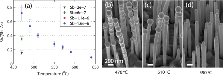
Figure 2. (a) The Sb composition data (calculated from XEDS analysis) for the ZB GaAs/GaAsxSb1−x core–shell nanowires grown at different temperatures (470–640 ° C), averaged over 3–5 nanowires for each sample. The blue circle and red square data points (respective Sb flux of 1.6 × 10⁻⁶ and 1.1 × 10⁻⁶ Torr) indicate formation of higher Sb-content shells at lower temperatures where below the temperature of 550 ° C, the shell growth is inhomogeneous. The green diamond and black triangle data points (respective Sb flux of 6 × 10⁻⁷ and 2 × 10⁻⁷ Torr) indicate formation of lower Sb-content shells at lower Sb fluxes with smooth side facets, confirming that the shell morphology is only affected by strain. 30° tilted view SEM images of GaAs/GaAsxSb1−x core–shell nanowires where the GaAsxSb1−x shells were grown at (b) 470 ° C, (c) 510 ° C and (d) 590 ° C. The scale bar for (c) and (d) is 200 nm.
Download figure:
Standard image High-resolution imageFigures 2(b)–(d) show SEM micrographs of the ZB GaAs/GaAsxSb1−x core–shell nanowires (with Sb flux of 1.6 × 10⁻⁶ Torr) grown at 470, 510, and 590 ° C, respectively. It should be mentioned that the nanowires grown at 550 ° C and higher temperatures demonstrate very similar morphology to those grown at 590 ° C (figure 2(d)). As shown in figures 2(b) and (c), by decreasing the temperature below 550 ° C the shell morphology starts to change, forming the rough side facets that indicate inhomogeneous shell growth, followed by some bending nanowires. Figure 2(b) shows the SEM image of the nanowires grown at 470 ° C, demonstrating significant inhomogeneous shell growth behavior. The formation of these rough side facets at low temperatures could be related to the strain induced from the high lattice mismatch between the GaAs cores and the GaAsxSb1−x shells, resulting in an island growth mode regime. Figure S1 of the supplementary material (available at stacks.iop.org/Nano/24/405601/mmedia) shows HAADF STEM and HRTEM images of such a nanowire. The same trend was observed for another similar set of samples grown with slightly lower Sb flux of 1.1 × 10⁻⁶ Torr, confirming the temperature effect on the composition and morphology of the nanowires. Our finding supports a recent report where similar surface roughening and island formation were observed in GaAs/GaSb core–shell nanowires [15]. Apart from the nanowire morphology, figures 2(b)–(d) also demonstrate significant tip morphology change for samples grown with low shell temperatures (below 570 ° C). This is shown by the overgrown faceted tips in figures 2(b) and (c). However, in this study we only focus on the nanowire core–shell morphology and the tip morphology change is beyond the scope of this work.
We next investigated the effect of Sb flux on the morphology of the grown core–shell nanowires. This series was performed at the lowest shell temperature of 470 ° C since we could not increase the Sb flux further. The results of this set of samples (green diamond, black triangle together with the blue circle data point at 470 ° C in figure 2(a)) indicate that the morphology of the grown nanowires (figure 2(b)) could be optimized (similar to figure 2(d)) by lowering Sb flux about one order of magnitude to Sb flux of 2 × 10⁻⁷ Torr. This morphology improvement at the constant shell growth temperature confirms that the shell morphology is only affected by strain (i.e. Sb-content) and not the temperature. Therefore, higher temperatures seem to reduce the available Sb, perhaps by increasing desorption.
Moreover, we have studied the growth rate of GaAsxSb1−x shells around ZB GaAs core nanowires. Figure 3 shows the nanowire diameter for samples grown with different shell growth times (0–45 min) where the error bars indicate the standard deviations from the average value. As the data suggest, GaAsxSb1−x shell growth rate follows a linear behavior, shown by dashed red line. Figure 3 suggests a quite high growth rate of ∼125 nm h−1, resulting from several processes such as the direct impingement of adatoms, their diffusion from the substrate, and contribution from the secondary adsorption process [16, 17].
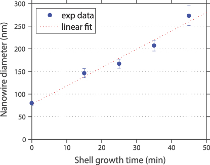
Figure 3. The GaAs/GaAsxSb1−x core–shell nanowire diameter for ZB samples grown with different shell growth times (0–45 min) shown by the blue data points. The GaAsxSb1−x shells are grown with Sb flux of 1.6 × 10⁻⁶ Torr at temperature of 570 ° C. The measurements were done on a minimum of 12 nanowires for each sample and the error bars indicate the standard deviation from the average values. The blue experimental data points suggest a linear shell growth rate shown by the dashed red line.
Download figure:
Standard image High-resolution image3.2. Effect of crystal phase
HRTEM investigations on the grown ZB nanowires clearly demonstrate that the GaAsxSb1−x shells follow the same stacking sequence as the GaAs core nanowire, as shown for other material systems [18]. As a result, the GaAsxSb1−x shell growth around ZB GaAs core nanowires result in the formation of ZB GaAsxSb1−x shells. It should be noted that the same trend has been observed in other core–shell nanowire material systems such as InAs/InP and GaP/Si [19, 20].
In addition to the ZB crystal structure, the GaAsxSb1−x shells were grown on WZ GaAs core nanowires as well. Although self-catalyzed GaAs nanowires normally adopt ZB phase, introducing a GaAsSb insert followed by shutting off Sb flux, and continuing the growth of GaAs allows the formation of WZ phase [5], as schematically shown in figure 4(a). We have used these WZ–ZB nanowires as a template to enable us to study the GaAsxSb1−x shell growth on both ZB and WZ crystal structures within the same nanowire.

Figure 4. Schematic illustration of (a) self-catalyzed GaAs/GaAsSb/GaAs core nanowires grown on Si(111) substrates. (b) Side view cross section of GaAs/GaAsSb/GaAs nanowires after Ga-solidification and GaAsxSb1−x shell growth. (c) 30° tilted view SEM image of GaAs/GaAsSb/GaAs core nanowires where Ga-solidification was performed at 640 ° C without Sb flux, resulting in GaAsSb insert decomposition, shown by white arrows. The scale bar is 100 nm. (d) 30° tilted view SEM image of GaAs/GaAsSb/GaAs nanowires with optimized solidification condition covered by GaAsxSb1−x shell grown for 25 min. The WZ segments have a visibly smaller diameter than the ZB segments, due to reduced radial growth. The scale bar is 100 nm.
Download figure:
Standard image High-resolution imageTo study the GaAsxSb1−x shell growth on the ZB–WZ GaAs nanowires, similar to the ZB GaAs nanowires, the Ga droplets were solidified after the core nanowire growth. Then, GaAsxSb1−x shells were epitaxially grown around the GaAs/GaAsSb/GaAs core nanowires, as schematically shown in figure 4(b).
The results of our study on the GaAs/GaAsSb/GaAs core nanowires indicate that applying the same Ga-solidification condition as used for the ZB GaAs core nanowires (supplying only As flux at 640 ° C) results in the decomposition of the GaAsSb inserts followed by nanowire thinning and kinking at the GaAsSb insert position. Figure 4(c) shows a SEM image of GaAs/GaAsSb/GaAs core nanowires with the same Ga-solidification condition (as compared to the ZB nanowires), resulting in GaAsSb decomposition indicated by white arrows. Therefore, to avoid this decomposition issue, Sb flux of 1.15 × 10⁻⁶ Torr was added during the solidification process and also the temperature was lowered to 550 ° C.
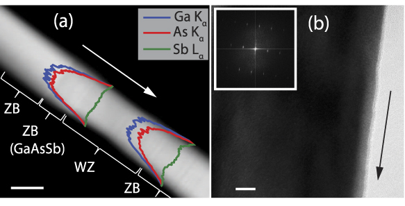
By employing the improved solidification condition, GaAsxSb1−x shells were then grown around the GaAs/GaAsSb/GaAs core nanowires. Figure 4(d) shows a SEM micrograph of such a sample with 25 min GaAsxSb1−x shell growth at 590 ° C and Sb flux of 1.1 × 10⁻⁶ Torr. Figure 5(a) shows a HAADF STEM image of a similar nanowire to those shown in figure 4(d), where the white arrow indicates the growth direction. As shown in figure 5(a), after the base GaAs ZB segment, a GaAsSb insert is introduced, which is followed by the formation of the GaAs WZ segment. It should be noted that after the WZ part, the crystal structure eventually changes back to ZB. The length of the GaAs WZ segment varies from 100 to 400 nm (after the GaAsSb insert) for nanowires with various diameters.
Figure 5. (a) HAADF STEM image of a similar nanowire (25 min shell growth) as shown in figure 4(d), demonstrating various segments along the nanowire where the white arrow shows the growth direction. The respective Ga, As and Sb signals are shown in blue, red and green colors where the shell composition is GaAs0.85Sb0.15. The antimony signal (green line) indicates homogeneous shell growth with slower growth rate on the WZ, compared to the ZB segment. The scale bar is 100 nm. (b) HRTEM image of the WZ segment for a sample with 15 min shell growth time, demonstrating WZ GaAsxSb1−x shell growth. The black arrow shows the growth direction and the scale bar is 10 nm. The inset shows the fast Fourier transform taken from the GaAsxSb1−x shell part, demonstrating the characteristic pattern of a hexagonal crystal phase.
Download figure:
Standard image High-resolution image
The radial XEDS line scans for both WZ and ZB segments are shown in the figure 5(a). The antimony signal (green line) indicates homogeneous shell growth on the WZ segment. Unlike the WZ segments, the shell growth is not homogeneous on the ZB segments due to the presence of polar microfacets that provide some nucleation sites. Also, the shell is thinner on the WZ, compared to the ZB segment. This is attributed to a slower GaAsxSb1−x shell growth rate on the WZ, compared to the ZB crystal structure as shown in other material systems [19]. A lower radial growth rate for WZ nanowires than for ZB has previously been attributed to a lower surface energy for WZ facets than for ZB [19, 21, 22], consistent with theoretical calculations of common WZ and ZB side facets [23]. This slower shell growth rate explains the thicker top part of the figures 4(d) and 5(a), corresponding ZB parts. It is difficult to accurately quantify the composition of the WZ shell since it is quite thin, but the Sb-content is measured to be similar to or slightly lower than on the ZB segment.
4. Conclusion
We have studied the growth of self-catalyzed GaAs/GaAsxSb1−x core–shell nanowires directly on Si(111) substrates by MBE technique. We demonstrate that by varying the temperature and Sb flux, the composition of the grown GaAsxSb1−x shells is tuned in a wide range, covering the miscibility gap. However, at low temperatures (below 550 ° C) and high Sb fluxes (≥1.1 × 10⁻⁶ Torr), the high lattice mismatch between the GaAs core and GaAsxSb1−x shells results in inhomogeneous shell growth. Furthermore, GaAsxSb1−x shells are successfully grown on both ZB and WZ core crystal structures. The morphological characterization results indicate that the shell growth rate is lower on the WZ, compared to the ZB segment, suggesting a lower side facet surface energy.
Acknowledgments
This work was partially supported by the Swedish Research Council (VR), the Swedish Foundation for Strategic Research (SSF), VINNOVA, the Knut and Alice Wallenberg Foundation (KAW), and the Nanometer Structure Consortium at Lund University (nmC@LU), and partially by the 'RENERGI' program of the Research Council of Norway under Grant No. 190871.