
Abstract
A plasma system with a complementary filter to shield samples from damage during tetrafluoromethane (CF4) plasma treatment was proposed in order to incorporate fluorine atoms into gadolinium oxide nanocrystals (Gd2O3-NCs) for flash memory applications. X-ray photoelectron spectroscopy confirmed that fluorine atoms were successfully introduced into the Gd2O3-NCs despite the use of a filter in the plasma-enhanced chemical vapour deposition system to shield against several potentially damaging species. The number of incorporated fluorine atoms can be controlled by varying the treatment time. The optimized memory window of the resulting flash memory devices was twice that of devices treated by a filterless system because more fluorine atoms were incorporated into the Gd2O3-NCs film with very little damage. This enlarged the bandgap energy from 5.48 to 6.83 eV, as observed by ultraviolet absorption measurements. This bandgap expansion can provide a large built-in electric field that allows more charges to be stored in the Gd2O3-NCs. The maximum improvement in the retention characteristic was >60%. Because plasma damage during treatment is minimal, maximum fluorination can be achieved. The concept of simply adding a filter to a plasma system to prevent plasma damage exhibits great promise for functionalization or modification of nanomaterials for advanced nanoelectronics while introducing minimal defects.
Export citation and abstract BibTeX RIS
1. Introduction
Since Tiwari et al [1] developed flash memory devices based on discrete charge traps such as metal nanocrystals (NCs) and semiconductor NCs embedded in a dielectric matrix, these devices have been extensively investigated in order to address the down-scaling issues of floating gate flash memory [2–4]. To achieve faster program/erase characteristics, control of the potential well depth (and thus the charge storage nodes) in metal NC memory, e.g., Ge, Au, Ag, Pt, and Ni has been demonstrated [5–7]. Moreover, metal–oxide NC flash memory using hafnium oxide NCs embedded in a SiO2 matrix reportedly exhibits good retention and endurance and a large memory window. In comparison with their metal NC counterparts, metal–oxide NC memory has advantages such as compatibility with complementary metal–oxide-semiconductor technology, rapid fabrication, and high trap densities [8, 9]. The structure of NCs embedded in a dielectric matrix has been controlled using various methods, such as sputtering followed by annealing [10], ion implantation [11], and self-assembly [12]. It was found that these processes can induce defects or traps in the dielectric matrix surrounding the NCs; this results in stored charge leakage from the NCs via trap-assisted tunnelling and causes retention problems [13, 14]. Therefore, the quality of the dielectric matrix, which electrically isolates the NCs, is critical to the construction of NC flash memory devices [15, 16]. Plasma treatment is a major step in ultralarge-scale integrated circuits and is used to passivate defects in the dielectric layer. It has been used to improve the reliability of NC flash memory devices because it enables passivation of traps or defects using hydrogen atoms [16] (in the case of hydrogen plasma) or nitrogen atoms [17] (in the case of ammonia plasma). Gadolinium oxide (Gd2O3), a rare-earth sesquioxide, has been reported to be a candidate as a gate dielectric for silicon and compound semiconductor device applications due to its low frequency dispersion, high k with high coupling ratio and process compatibility with easy fabrication for NCs formation [18–20]. The crystallized Gd2O3-NCs with low bandgap energy (Eg ∼ 5.0–5.4 eV) surrounded by the high Eg of amorphous Gd2O3 dielectric (∼6.3–6.4 eV) to perform the energy band offset are responsible for the charge storage [21, 22]. Unfortunately, there is still room for improving the memory characteristics of Gd2O3-NC based flash memory. In our previous study [23, 24], we fluorinated Gd2O3-NCs for NC-based flash memory by using tetrafluoromethane (CF4) plasma treatment. The memory characteristics, including the program/erase speed, charge retention, and endurance, were significantly improved by the incorporation of fluorine atoms, resulting in a built-in electric field in the Gd2O3 nanostructure. However, defects are inevitably introduced into the dielectric matrix when a plasma is applied, owing to plasma damage resulting from energetic ion bombardment and ultraviolet (UV) irradiation [25–27]. This damage may counterbalance the passivation effect because of additional defects induced by the plasma. In this study, we propose the insertion of a filter into the plasma-enhanced chemical vapour deposition (PECVD) system as a shield against species that degrade the dielectric matrix surrounding the NCs so as to achieve a low-damage plasma treatment. When this filter was used, the CF4–plasma-treated Gd2O3-NC flash memory exhibited an enhanced memory window (more than twice as high as the previous optimized result without the filter) and greater data retention because more fluorine atoms could be introduced into the Gd2O3-NC nanostructure with minimal damage.
2. Experimental details
2.1. Sample preparation
The fabrication of a Gd2O3-NC flash memory device is shown schematically in figure 1. After an n-type (100) silicon wafer received the standard RCA wafer cleaning process, a 3 nm thick tunnel oxide was thermally grown in a horizontal furnace. Next, a 10 nm thick amorphous Gd2O3 layer was deposited by sputtering with a Gd (99.9% pure) target in an oxygen (O2) and argon (Ar) mixture ambient at room temperature. The flow rates of O2 and Ar were 3 and 21 sccm, respectively. After the dielectric films formed, the samples were treated by rapid thermal annealing (RTA) at 900 °C for 30 s in nitrogen ambient to form the Gd2O3-NCs. The samples were then treated using a low-damage CF4 plasma in a PECVD system with a complementary quartz filter near the substrate, as shown schematically in figure 2(a). As shown in figure 2(b), the quartz filter consists of upper and lower plates separated by a quartz spacer. Both plates contain many stripes and slits of the same width. The slits of the upper plate are aligned with the stripes of the lower plate. One side of the upper plate is coated with a thin metal film. The filter is placed on a supporter coated with an insulating material so that energetic ions can be confined to the plasma area between the upper electrode and the filter [28]. In this arrangement, the filter can efficiently shield the sample from plasma damage caused by energetic electrons, energetic ions, and UV photons. It permits only neutral and reactive radicals to diffuse through the filter and reach the heated substrate (300 °C), thus realizing a low-damage plasma treatment procedure. In pure CF4 plasma, the radicals are primarily fluorine radicals with a small concentration of complex fluorocarbon species [29]. As a result, Gd2O3-NC films can be effectively fluorinated with minimal plasma damage. Radio frequency (RF) power (100 W, 13.56 MHz) was applied to the upper electrode through a matching box. The base pressure of the PECVD was less than 1 × 10⁵ Torr, and the process pressure was maintained at 500 mTorr. To confirm that the filter reduced the UV irradiation, optical emission spectroscopy (OES) with a quartz lens was used to measure the optical emission between the filter and the substrate through a quartz window on the side wall of the PECVD system, aimed into a fibre bundle. The emission at the same position was also measured when the filter was not inserted into the PECVD system. Figure 2(c) shows the emission spectra in the UV range with and without the filter. After the filter was inserted, the UV photon intensity decreased dramatically. By calculating the area under the spectra, we found that more than 95% of the UV photons can be eliminated. According to [28] and the OES results, we believe that plasma damage resulting from energetic ions and UV irradiation can be efficiently eliminated. After CF4 plasma treatment, a SiO2 film serving as a blocking oxide was deposited by PECVD on all of the samples using SiH4 (5 sccm) and N2O (200 sccm) mixed gases at 300 °C. Finally, a 300 nm aluminum film was deposited by a thermal coater on both sides of the samples, and a gate on the blocking oxide was defined by lithography and wet etching.
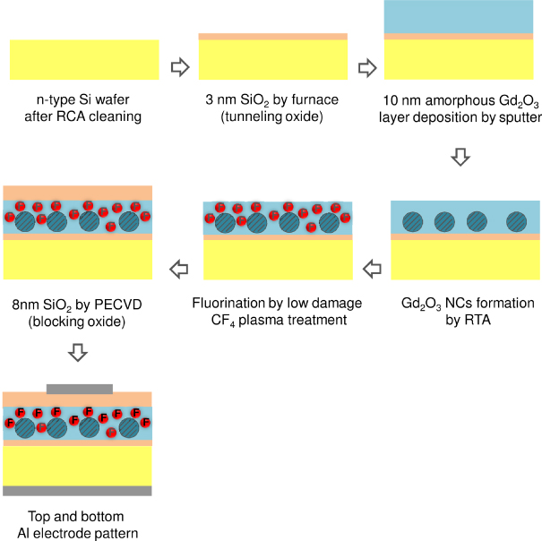
Figure 1. Fabrication flow of Gd2O3-NC flash memory device.
Download figure:
Standard image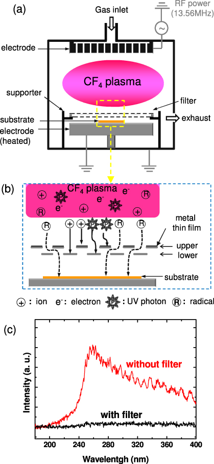
Figure 2. (a) Schematic of PECVD system with the filter, (b) enlarged view of quartz filter, and (c) optical emission spectroscopy of CF4 plasma with and without the filter at various RF powers.
Download figure:
Standard image2.2. Material characterization
X-ray spectroscopy (XPS) was used for material analysis of the fluorinated Gd2O3-NC films. UV absorption spectra of the films at 150–350 nm were measured with light from a synchrotron source. The light was dispersed from a high-flux beamline with a 6 m cylindrical grating monochromator coupled to the 1.5 GeV storage ring at the National Synchrotron Radiation Research Centre in Taiwan. In this work, incident light with a resolution of 0.5 nm and intensity of 1.2 × 10⁶ photons s−1 was conducted through a gold mesh with about 90% transmission; subsequently, the photocurrent of the gold mesh was detected by an electrometer (Keithley 6512) for monitoring and normalization of the beam. The light transmitted through the sample impinged on a glass window coated with sodium salicylate, the fluorescence of which was detected by a photomultiplier tube (Hamamatsu R943) in photon-counting mode. For UV absorption measurements, a fluorinated Gd2O3-NC film was prepared on a fused quartz substrate. The absorption of the film was determined by the following formula [30]:

where α is the absorption coefficient, d is the film thickness, and I0 and I are the intensity of transmitted photons through the quartz substrate and the Gd2O3-NC film/quartz substrate, respectively.
Atomic force microscopy (AFM) and high-resolution transmission electron microscopy (HRTEM) observations were also made to observe the nanostructure of the Gd2O3-NC films. For AFM measurement, the root-mean-square Rrms was calculated from surface height data zi obtained from a 1 μm × 1 μm scanning area using numerical integration and the following relationships:

where N is the number of surface height data (i.e. N = 512 × 512 = 262,144) and  is the mean-height distance [31]. For electrical analysis, the capacitance–voltage (C–V) hysteresis was measured using an HP4285 precision LCR meter to obtain the memory window. At least five samples were prepared for each measurement.
3. Results and discussion
3.1. Material characterization of fluorinated Gd2O3-NC films
HRTEM was used to observe the structure of the Gd2O3-NCs after amorphous Gd2O3 layer deposition followed by RTA and low-damage CF4 plasma treatment for 10 min. As shown in figure 3(a), the Gd2O3 NCs embedded in an amorphous Gd2O3 dielectric layer were clearly visualized by HRTEM. The Gd2O3 NCs were around 5 nm in size. The grain boundary material between Gd2O3-NC and amorphous Gd2O3 may exhibit a silicate phase, which was observed in our previous study [32]. Figure 3(b) displays tapping mode 3D AFM images and the estimated surface roughness of Gd2O3-NC films for various low-damage plasma treatment times. For treatment times of less than 10 min, the Rrms increased only slightly, which means that the low-damage plasma treatment has almost no effect on the surface roughness. For a treatment time of 30 min, Rrms increased significantly (more than 20%), indicating that some plasma damage occurred at the film surface after lengthy treatment.

Figure 3. (a) HRTEM image of Gd2O3-NC film after low-damage CF4 plasma treatment for 10 min; (b) AFM images of Gd2O3-NC film after low-damage CF4 plasma treatment for various treatment times.
Download figure:
Standard imageXPS was used to confirm the incorporation of fluorine atoms into the Gd2O3-NCs subjected to low-damage CF4 plasma treatment. Figure 4 shows XPS spectra of the Gd2O3-NCs after treatment for different times in the F 1 s region after using the Shirley method to subtract the background. Peaks were clearly observed, and the peak intensity increased as the treatment time increased, which indicates that fluorine atoms can be introduced into the nanostructure and that the number of incorporated fluorine atoms can be controlled. In comparison with our previous optimized condition for memory characteristics [24], we found that many more fluorine atoms can be incorporated into the Gd2O3-NC films, yielding highly fluorinated films. Figure 4 also shows the peak deconvolution with two Gaussian profiles for all XPS spectra at F 1 s. The main peak at a binding energy of ∼685.5 eV corresponds to the formation of Gd-F indicating the fluorination of the Gd2O3-NC film. The other peak at a binding energy of ∼688.0 eV with small intensity corresponds to C–F bonding, possibly due to the residue of fluorocarbon during CF4 plasma treatment. Such a kind of organic residue can be easily removed by high-temperature annealing.
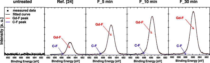
Figure 4. XPS spectra in the F 1 s region of Gd2O3-NC film after low-damage CF4 plasma treatment for various treatment times.
Download figure:
Standard imageSome researchers have reported that fluorine atoms in dielectric films will expand the bandgap owing to their high electronegativity [33, 34]. Therefore, we also investigated the UV absorption to determine the optical Eg of the fluorinated Gd2O3-NC films. Figure 5(a) shows the absorption coefficients of the films, calculated from the vacuum UV absorption spectra, as a function of plasma treatment time. The absorption edge of the films clearly depends on the plasma treatment time and shows a large blueshift when the plasma treatment time increases. The result is attributed to the incorporation of more fluorine atoms, which expands Eg because of the high electronegativity of fluorine atoms. To determine the optical Eg of the fluorinated Gd2O3-NC films, we used the Tauc formula [35, 36],
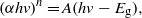
where A is a constant, h is Planck's constant, v is the frequency, and n is 2 in the case of direct allowed and forbidden electronic transitions. We plotted (αhv)2 versus the photon energy (hv), as shown in figure 5(b). These plots have a distinct linear region that indicates the onset of absorption. Therefore, extrapolating this linear region to the abscissa, which represents (hv), yields the Eg value of the fluorinated Gd2O3-NC films. Table 1 displays the fitting region of each plasma treatment time and its coefficient of determination (R2) and extracted Eg. We found that the Eg values of fluorinated Gd2O3-NC films increased significantly when the plasma treatment time increased. These Eg values of fluorinated Gd2O3-NC films treated by low-damage CF4 plasma treatment are all greater than those obtained after optimized plasma treatment in our previous study because more fluorine atoms can be successfully incorporated into Gd2O3-NC films, as shown by the XPS results (see figure 4).
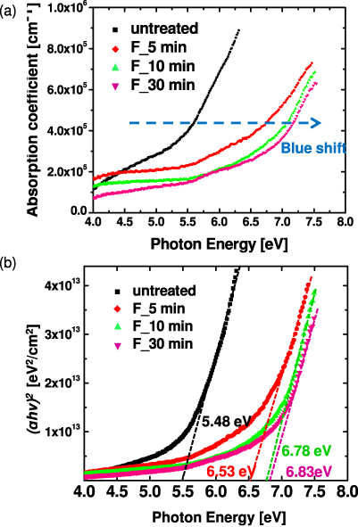
Figure 5. (a) Absorption spectra and (b) Tauc plots of Gd2O3-NC films treated with low-damage CF4 plasma for various treatment times.
Download figure:
Standard imageTable 1. Linear least square fitting of Tauc plots and the determined Eg values of Gd2O3-NC films treated by low-damage CF4 plasma treatment.
| Treat. time (min) | Linear region (eV) | Coefficient of determination (R2) | Bandgap energy, Eg (eV) |
|---|---|---|---|
| 0 (untreated) | 5.85–6.25 | 0.993 | 5.48 ± 0.13 |
| 5 | 7.00–7.40 | 0.991 | 6.53 ± 0.15 |
| 10 | 7.10–7.50 | 0.996 | 6.78 ± 0.09 |
| 30 | 7.15–7.55 | 0.998 | 6.83 ± 0.07 |
3.2. Electrical characteristics of fluorinated Gd2O3-NC flash memory devices
Figure 6 shows representative C–V hysteresis curves of fluorinated Gd2O3-NC flash memory devices fabricated using low-damage CF4 plasma treatment. The gate voltage was swept from −10 to 10 V and then back. The hystereses of the fluorinated devices are all significantly wider than that of the untreated device. To quantitatively compare the memory window, all the memory windows were extracted at 0.6Cox from their respective C–V curves and displayed in table 2. An optimized memory window (∼2.3 V) was obtained for a plasma treatment time of 10 min. In comparison with the sample that did not undergo CF4 plasma treatment, the memory window improved more than twofold. The results are significantly better than that using a filter-less plasma system. XPS depth profile analysis in our previous study [23, 24] showed that the fluorine intensity was greatest at the Gd2O3-NC film surface and decreased with increasing film depth. As mentioned in section 3.1, incorporation of fluorine atoms increases the Eg of Gd2O3-NC film. The more fluorine atoms incorporated into the Gd2O3-NC film, the larger the Eg obtained. On the basis of this finding, we proposed a gradual nanostructure energy band diagram, i.e., larger Eg near the blocking oxide and smaller Eg near the tunnelling oxide, of Gd2O3-NC memory. This is believed to generate a built-in electric field in the Gd2O3-NC films, preventing injected charges from the tunnelling oxide from flowing through the blocking oxide to the gate. Consequently, many charges can be stored in the Gd2O3-NCs, yielding a larger memory window. Because more fluorine atoms can be incorporated into the Gd2O3 layer using our proposed low-damage CF4 plasma treatment, as shown in figure 4, a higher Eg and thus a larger built-in electric field can be obtained, as demonstrated in figure 5. As a result, it is more difficult for charges to flow through the blocking oxide to the gate, and the memory window is larger. For a treatment time of 30 min, the memory window decreased even though the fluorine intensity was the highest. The reason may be the surface roughness. A rough surface can reportedly induce interface states, lowering the interface barrier [37–40]. Consequently, the leakage current can be enhanced at a rough surface but not at a smooth one. Furthermore, the optimized memory window in our previous study was only 1.03 V (RF power: 50 W; treatment time: 1 min), as indicated by the C–V hysteresis curve shown in figure 6(a). It is noteworthy that the memory window of the sample with the optimized low-damage plasma condition recorded in the current study is further improved by more than twofold over the window obtained under an optimized plasma condition [24]. We also performed CF4 plasma treatment for longer times and at higher RF powers (50 W for 5 min and 100 W for 1 and 3 min) without the filter to incorporate more fluorine atoms into the Gd2O3-NC film; however, the resulting memory devices did not function. This is attributed to plasma damage that caused defect states in the film, leading to leakage of stored charge from the film via trap-assisted tunnelling and eliminating the memory window. In addition, the samples were not treated by annealing after the low-damage CF4 plasma treatment, which was required in our previous study.
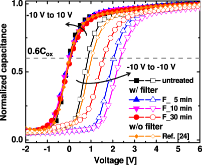
Figure 6. (a) C–V hysteresis curves and (b) memory windows of Gd2O3-NC flash memory devices after low-damage CF4 plasma treatment for various treatment times.
Download figure:
Standard imageTable 2. Memory windows and charge loss rates of samples treated by CF4 plasma with and without the filter with various treatment time.
| Samples | Memory window (V) | Charge loss rate (×10−3 s−1) | Charge loss (%) | |
|---|---|---|---|---|
| Shallow trap (ST) | Deep trap (DT) | |||
| Untreated | 0.86 | 9.5 | 0.5 | 14.1 |
| w/filter | ||||
| 5 min | 1.70 | 6.3 | 0.4 | 9.4 |
| 10 min | 2.03 | 0.8 | 0.4 | 4.8 |
| 30 min | 2.33 | 2.1 | 0.6 | 9.0 |
| w/o filter [24] | ||||
| 1 min | 1.11 | 8.5 | 0.6 | 13.0 |
| 3 min | N/A | 16.7 | 0.6 | 24.1 |
Figure 7 shows the room-temperature retention characteristics of the low-damage CF4-treated Gd2O3-NC flash memory devices. For comparison, the characteristic of devices treated by CF4 plasma without the filter in our previous study [24] are also included. In the case of CF4 plasma treatment without the filter, the charge loss of the devices improves slightly after 1 min treatment (optimized plasma treatment condition), owing to Eg expansion, and the charge loss becomes significantly worse after 3 min treatment. It is noteworthy that the retention curves can be approximately divided into two regions that have different loss rates. The higher initial charge loss rate is observed from 0 to 1000 s, while a lower charge loss rate is observed from 1000 to 10 000 s. In our previous studies [24, 41], we have concluded that the former region of charge loss curve is associated with charge loss from shallow traps (ST) in the Gd2O3-NC film, while the latter one is associated with charge loss from deep traps (DT) via a direct tunnelling to the interface state at the SiO2/Si interface. In addition, shallow-trap charge loss reportedly results from defect generation in the dielectric layer [42, 43]. The charge loss rates of ST and DT can be obtained by linear fitting in the respective regions. The fitted charge loss rates are shown in table 2. We can clearly see that the charge loss rate after 3 min treatment in the ST region is much higher than that after 1 min treatment, while both charge loss rates in the DT region are almost the same. Because the ST charge loss corresponds to defect generation, we considered that the longer plasma treatment time causes plasma damage leading to many defects in the Gd2O3-NC films, resulting in current leakage due to trap-assisted tunnelling [13, 14]. In the case of the low-damage CF4-treated Gd2O3-NC flash memory devices, as the treatment time increased, the charge loss decreased because more fluorine atoms were incorporated into the Gd2O3-NC film with minimal defect generation, which not only produced a larger Eg to prevent charge loss through the blocking oxide but also minimized the trap-assisted tunnelling. However, after a 30 min treatment, the charge loss increased. We attributed this to the rough surface, which gives rise to interface states and leakage current, i.e., charge loss. In this study, the optimized treatment time was 10 min. Regardless of treatment time, the charge losses of devices treated with the filter clearly exhibited great improvement and were significantly superior to those of samples treated without the filter. Table 2 shows the charge losses at 104 sec in devices that received plasma treatment with and without the filter. A comparison between both optimized results shows the maximum improvement of more than 60%. As shown in table 2, we can see that the charge loss rate of samples treated with the filter in the region of ST are much smaller than that of samples treated without the filter while the charge loss rates of both kinds of samples are almost the same. We can conclude that the improvement of charge loss is mainly due to the reduction of ST, because low-damage CF4 plasma treatment causes only minimal plasma damage, i.e., minimal defect generation, in the Gd2O3-NC films, which can maximize the effect of fluorination of the films to obtain large Eg expansion and little charge loss. These results further prove that low-damage CF4 plasma treatment during the fabrication of fluorinated Gd2O3-NC flash memory devices can be realized using our proposed method.
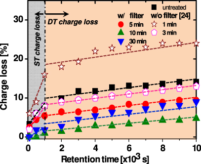
Figure 7. (a) Room-temperature charge retention characteristics of Gd2O3-NC flash memory devices. Inset shows the enlargement of the charge retention curves to demonstrate the different linear slopes between ST and DT. Solid symbols represent devices fabricated in this study; open symbols represent those fabricated in our previous study [24]. (b) The charge loss rates of Gd2O3-NC flash memory devices treated by CF4 plasma with and without the filter for shallow-trap and deep-trap charge losses.
Download figure:
Standard image4. Conclusions
In summary, low-damage CF4 plasma treatment in a PECVD system with a filter was proposed to introduce fluorine atoms into Gd2O3-NCs. HRTEM clearly demonstrated Gd2O3-NCs embedded in an amorphous Gd2O3 layer after the low-damage plasma treatment. The treatment had almost no effect on the surface roughness of the Gd2O3-NC films at treatment times of less than 10 min; however, an increase of around 20% was observed for a treatment time of 30 min. XPS confirmed that fluorine atoms were successfully introduced into the Gd2O3-NCs despite the presence of a complementary filter in the PECVD system to shield samples from several potentially damaging species. The number of fluorine atoms incorporated into the Gd2O3-NCs can be controlled by varying the CF4 plasma treatment time. The incorporation of fluorine atoms into the films enlarged Eg from 5.48 to 6.83 eV, as determined by UV absorption measurements and Tauc plots. The optimized memory window of flash memory devices based on fluorinated Gd2O3-NCs treated by our proposed system was twice that of devices based on films treated by a filter-less system. The reason is that the proposed system enables the incorporation of more fluorine atoms into the Gd2O3-NCs film to further enlarge the bandgap with minimal damage. The resulting bandgap expansion can produce a large built-in electric field that allows more charge to be stored in the Gd2O3-NCs. Moreover, the maximum improvement in the retention characteristic was more than 60% owing to a reduction in shallow-trap charge loss. Because low-damage CF4 plasma treatment causes only minimal plasma damage to the Gd2O3-NC films, the maximum effect of fluorination can be achieved. The concept of simply adding a filter to a plasma system to prevent plasma damage exhibits great promise for functionalization or modification of nanomaterials for various advanced nanoelectronics while imposing minimal defects.