
Abstract
In this paper, we demonstrate a new catalyst (Fe) to grow single crystalline beta-gallium oxide (β-Ga2O3) nanowires (NWs) via the vapour–liquid–solid mechanism using the chemical vapour deposition technique. The structural studies of these NWs showed the highly crystalline monoclinic phase of Ga2O3. This was confirmed by detailed scanning transmission electron microscope investigations demonstrating the NW to be single crystalline β-Ga2O3, growing along the normal of the  plane. We also compared Raman and cathodoluminescence (CL) properties of the as-grown β-Ga2O3 NWs with a bulk Ga2O3 single crystal grown by the Czochralski method. It was observed that Raman peak positions of a single β-Ga2O3 NW had a red frequency shift of about 0.3–1.4 cm−1 as compared to a bulk Ga2O3 single crystal, which was in fact quite small. In addition, the CL measurements of β-Ga2O3 NWs and the bulk Ga2O3 single crystal exhibited similar spectra, having a strong broad UV–blue emission band and a weak red emission band. Moreover, the structural, morphological and optical properties of Fe-catalysed β-Ga2O3 NWs were comparable to those of Au-catalysed β-Ga2O3 NWs.
Export citation and abstract BibTeX RIS
1. Introduction
Monoclinic gallium oxide (β-Ga2O3) has excellent thermal and chemical stability from room temperature (RT) up to 1400 °C in oxidizing conditions [1–3]. Above this temperature it is neither thermally nor chemically stable and it simply decomposes even in the presence of oxygen [4]. It has a wide bandgap with optical bandgap (Eg) of 4.9 eV at RT [5, 6]. It is optically transparent in the region of the ultraviolet (UV) to visible spectrum, which makes it useful in optoelectronic devices, including flat panel displays, solar energy conversion devices and optical limiters for UV [7, 8]. In addition, the thermal stability of β-Ga2O3 has been utilized in the fabrication of high temperature stable gas sensors [9, 10]. Furthermore, low dimensional, crystalline nanostructures such as nanowires (NWs), nanobelts (NBs) and nanosheets (NSHs) of Ga2O3 have been of particular interest to many research groups in the past 10 years or so due to their applications in various novel nanodevices, including nanowire based field effect transistors (NW-FETs) [11, 12], gas sensors [13–15], solar blind photodetectors [16, 17] and nanoswitches [18].
Ga2O3 nanostructures are generally grown using a bottom-up approach, which includes physical evaporation [19], arc discharge [20], laser ablation [21], carbothermal reduction [22], chemical vapour deposition (CVD) [23], metal–organic CVD (MOCVD) [24, 25], microwave plasma reaction [26] and vapour phase epitaxy (VPE) [27] techniques. The vapour–liquid–solid (VLS) and vapour–solid (VS) growth mechanisms are mostly used to explain β-Ga2O3 nanostructure growth [28–30]. In general, β-Ga2O3 NWs are grown utilizing Au as a catalyst, but inadvertent incorporation of Au inside the β-Ga2O3 lattice during growth may lead to formation of deep level impurities inside the semiconductor. These deep level impurities may degrade the performance of optoelectronic and electronic devices fabricated using these NWs. However, the other semiconductor NWs such as ZnO and Si have been grown using various transition metal (Fe and Ni) catalysts [31, 32]. Moreover, Fe has been used commonly in the catalytic growth of 1D carbon nanotubes. In spite of Fe being used to grow various metal oxide NWs, there are few reports available related to the growth of β-Ga2O3 NWs where Fe served as catalyst [33]. In our previous studies, we used noble metal (Au) as a catalyst to grow β-Ga2O3 NWs [34, 35]. In the present study, we explored an alternative catalyst to grow β-Ga2O3 NWs and their detailed investigations, including an atomic structural model of β-Ga2O3, elemental mapping and line scan profile on a single NW. Another new aspect of this work is a comparative study of structural and optical properties of Fe-catalysed β-Ga2O3 NWs and a bulk Ga2O3 single crystal grown by the Czochralski method at IKZ, Berlin [4]. In all the previous Raman comparative studies, Ga2O3 powder was used to compare with Ga2O3 NWs/NBs [36–38].
In this paper, β-Ga2O3 NWs were synthesized by the CVD technique at a temperature of 950 °C on Fe-coated sapphire substrates using argon (Ar) as a carrier gas. We have carried out a comprehensive study of various properties of the thus grown β-Ga2O3 NWs. For characterizing the morphology and size of the nanostructures scanning electron microscopy (SEM) was employed. The integral structural analysis was carried out using XRD, x-ray photoelectron spectroscopy (XPS) and Raman spectroscopy. The detailed atomic structure and chemistry was identified by scanning transmission electron microscopy (STEM) and energy-dispersive x-ray spectroscopy (EDXS). Furthermore, the optical properties of β-Ga2O3 NWs were investigated utilizing cathodoluminescence (CL) spectroscopy.
2. Experimental section
2.1. Synthesis of nanowires
First of all, an ultra-thin film of Fe (~5 nm) was deposited on the sapphire (c-plane) substrate under a vacuum of 10–5 Torr by the thermal evaporation technique. Thereafter, in order to grow β-Ga2O3 NWs, a small quantity (~500 mg) of Ga metal with a purity of 99.999% (Aldrich) was taken as the precursor and placed in a quartz boat, and Fe-coated substrates were clipped over the boat. The total system was loaded in the centre of a quartz tube. The quartz tube was placed inside a tubular furnace at a temperature of 950 °C for 3 h. A constant flow of argon (Ar) gas was maintained in the quartz tube during the growth process. The heating and cooling rate of the furnace was 10 °C min−1. After completion of the process, the power of the CVD system was switched off and the system cooled down naturally. Finally, a white wool-like thin film was deposited over the substrates, which was further characterized using various techniques.
2.2. Characterization
The determination of morphology and CL measurements (MonoCL3 from Gatan) in the UV–visible spectral range were performed in an SEM (Hitachi S-4800) at RT with electron beam energy of 5 keV. The crystal structure of the β-Ga2O3 NWs was characterized with x-ray diffraction (XRD) and STEM. The XRD measurements were made with a Philips Xpert Pro using Cu Kα (λ = 1.5405 Å) radiation in the 2θ range 20–80°. For TEM, selected area electron diffraction (SAED), high-resolution STEM and EDXS measurements a probe Cs-corrected FEI-TITAN 80/300 was employed, which was operated at 300 kV. The Raman measurements were made at RT in the backscattering configuration using a LabRam HR800 spectrometer from Horiba JobinYvon. A linearly polarized laser emitting at 532 nm was employed for the Raman excitation. The laser light was tightly focused by a 100 × objective (numerical aperture 0.9) corresponding to a diameter of the normally incident probing beam of ~0.8 µm and to a laser power on the sample surface of ~353 µW using a filter resulting in a power density of only ~70 kW cm−2. Micro-Raman spectra of individual β-Ga2O3 NWs showed no structural damage or additional Raman shift due to local heating by the laser beam. The same measurement procedure was applied to a bulk Ga2O3 single crystal for comparison purposes. To determine the chemical composition of the surface of as-grown NWs, XPS was utilized. The core level and valence band photoelectron spectra were excited by monochromatic Al Kα radiation (1487 eV) and minimize the effect of x-ray damage due to the sample collected with an adjustable overall resolution between 0.8 and 1.2 eV. Photoelectrons were picked up at a takeoff angle of 35°, enhancing the surface sensitivity of the technique to about 10–15 Å depth. Samples were first scanned from 0 to 1200 eV to monitor signals for Ga and O. The Ga 2p at 1110–1160 eV and O 1s at 520–550 eV were investigated in detail. Scan times of up to ∼2 h were employed for all data collections. Data analysis was performed using the Sigma Probe Advantage software. Precise binding energy positions and intensities were calculated by peak fitting using a software package (XPSPEAK version 4.1). Peak fitting solutions were sought for χ2 < 1, where χ2 stands for the standard deviation. The observed binding energy of the Ga 2p3/2 bulk signal allows determination of the difference between the Fermi level and the energy of the valence-band maximum at the surface. The integral areas under specific peaks of the XPS spectra can be normalized to the integral under the Ga 2p peak (sum of Ga 2p1/2 and Ga 2p3/2) and adjusted with respect to scan time. The reflectance was measured using a UV–VIS–NIR spectroscope from Perkin Elmer (model Lambda 1050)..
3. Results and discussion
3.1. Morphological studies of β-Ga2O3 NWs
3.1.1. SEM and EDXS analysis.
The general morphology of Fe-catalysed β-Ga2O3 nanostructures, which consist of mainly NWs and NBs at low and high magnification, is presented in figures 1(a)–(d). The statistical analysis including errors in the diameter of NWs is depicted via a diameter histogram in the inset of figure 1(a). The diameters of approximately 100 NWs are in a range of 30–80 nm with an average of 55 ± 3 nm, and the lengths of most of these NWs are tens of micrometers. In addition, the width of β-Ga2O3 NBs is in the range of 150–400 nm and their lengths up to 30 μm. At higher magnification (figure 1(d)), the nanoparticles at the tip of the NWs are clearly visible. This verifies that the growth of β-Ga2O3 NWs is based on the VLS mechanism and it is further confirmed by TEM measurements. Zhu et al [32] studied Au, Ni and Fe-catalysed growth of ZnO NWs. They observed that the diameter of NWs was insensitive to the thickness of Fe thin film, whereas the diameter of NWs was dependent on the thickness of Au and Ni thin films. Therefore, they suggested that, in the case of Fe catalyst, NWs did not grow via the VLS growth process. The binary phase diagram of Fe and Ga, which demonstrates the compositional zone responsible for alloying, nucleation and growth can be seen in [39].

Figure 1. (a)–(b) Low magnification SEM images of as-grown Fe-catalysed β-Ga2O3 nanowires and (c)–(d) high resolution SEM images of the nanowires.
Download figure:
Standard image High-resolution imageEDXS analysis was further performed to determine the concentration of Ga and O in the as-grown β-Ga2O3 NWs. Besides the strong Ga and O signals, some small peaks are apparent corresponding to the Fe catalyst and carbon coating during EDXS measurements.
3.2. Structural analysis of β-Ga2O3 NWs
3.2.1. XRD analysis.
The XRD investigation was used to obtain the basic information about the structure and phase purity of as-grown β-Ga2O3 NWs on sapphire substrate using Fe as a catalyst. Various closely spaced peaks indexed to the monoclinic phase of Ga2O3 are illustrated in figure 2, and are in good agreement with the reported values of β-Ga2O3. These peaks are recognized according to Joint Committee for Powder Diffraction Standards (JCPDS) Card No. 11-0370. Miller indices (hkl) of β-Ga2O3, including (004),  (111), (104),
 (003),
  (311), (020), (017), (402) and
  are assigned in this present pattern. This XRD pattern reveals that no other crystalline modifications or impurities are present within the 2θ range (20–80°). The strong intensities of β-Ga2O3 diffraction peaks indicate that the resulting product (as-grown NWs) is monoclinic Ga2O3.

Figure 2. XRD patterns of β-Ga2O3 nanowires grown on sapphire using Fe as a catalyst at 950 °C for 3 h.
Download figure:
Standard image High-resolution image3.2.2. TEM and STEM analyses.
Furthermore, to elucidate details of the morphology, structure and chemical composition of as-grown Fe-catalysed β-Ga2O3 NWs, we carried out TEM, STEM and EDXS investigations. The TEM image in figure 3(a) shows an overview of as-grown NWs demonstrating their general morphology. In figure 3(b) a cutout of (a) is magnified. A single NW is characterized, which ends in a particle. The SAED pattern (figure 3(c)) from the NW corresponds to the ![$[1\text{}\text{ \bar{1}}\text{ 2}]$](https://content.cld.iop.org/journals/0022-3727/47/43/435101/revision1/d501383ieqn007.gif) zone axis pattern of β-Ga2O3 and indicates
zone axis pattern of β-Ga2O3 and indicates ![$[1\text{}\text{ \bar{3}}\text{ \bar{1}}\text{ \bar{8}}]$](https://content.cld.iop.org/journals/0022-3727/47/43/435101/revision1/d501383ieqn008.gif) as the growth direction, which corresponds to the normal of the
as the growth direction, which corresponds to the normal of the  plane. In agreement with XRD analysis, SAED shows that the as-grown NWs are single crystalline and have no other impurities or phases present.

Figure 3. (a) Overview of β-Ga2O3 nanowires in TEM diffraction contrast; (b) magnified cut-out framed in (a) showing a single nanowire with a catalyst particle at its top. (c) The selected area diffraction pattern (taken on the nanowire) demonstrates the ![$[1\text{}\text{ \bar{1}}\text{ 2}]$](https://content.cld.iop.org/journals/0022-3727/47/43/435101/revision1/d501383ieqn010.gif) zone axis pattern of β-Ga2O3 which shows the normal of the
zone axis pattern of β-Ga2O3 which shows the normal of the  plane as the fibre axis.
Download figure:
Standard image High-resolution imageThe STEM investigations clearly demonstrate that the single NW consists of the monoclinic phase of Ga2O3. The wire shows a segmented shape indicated by slight constrictions of the surface in annular dark-field-STEM (ADF-STEM). The atomic structure of the Fe-catalysed NWs was further characterized by ADF-STEM (see figure 4). The atomic structure image shows the atomic arrangement in ![$[1\text{}\text{ \bar{1}}\text{ 2}]$](https://content.cld.iop.org/journals/0022-3727/47/43/435101/revision1/d501383ieqn012.gif) orientation without any structural defects.
orientation without any structural defects.
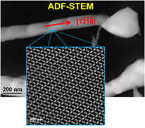
Figure 4. Annular dark-field scanning transmission electron microscope (ADF-STEM) image of the β-Ga2O3 nanowire with a zoomed in area framed on the nanowire, which illustrates the atomic structure of β-Ga2O3 in ![$[1\text{}\text{ \bar{1}}\text{ 2}]$](https://content.cld.iop.org/journals/0022-3727/47/43/435101/revision1/d501383ieqn013.gif) orientation.
orientation.
Download figure:
Standard image High-resolution imageFurther, the chemical composition of as-grown β-Ga2O3 NWs was investigated by STEM-EDXS. The EDXS elemental maps are shown in figures 5(b)–(d), illustrating the spatial distributions of Ga (blue), O (orange) and Fe (green). It is clearly noticed that Ga and O are roughly homogeneously distributed throughout the NW and nanoparticle, whereas Fe is agglomerated at the NW tip. Furthermore, the EDXS line profiles show that the NW consists of Ga and O, whereas in the particle Fe is also detected. In addition, EDXS profiles of the integrated intensities of the signals of O K, Ga K, and Fe K lines were measured at points along lines across the NW (see figures 6(a) and (b)), across the particle (figures 6(c) and (d)) and across the interface between the wire and the nanoparticle (figures 6(e) and (f)). Obviously, the distributions of Ga and Fe develop in reverse from the left to the right in the particle, which indicates an interdiffusion of Ga and Fe between wire and particle. In contrast to Ga and Fe, O appears to be roughly homogeneously distributed, as already shown in the EDXS maps in figure 5.
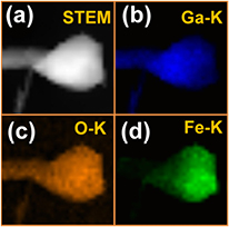
Figure 5. (a) ADF-STEM image of a selected nanowire tip with a catalyst particle and (b)–(d) corresponding mapping of the integrated intensities of the EDXS signals for Ga (blue), oxygen (orange) and Fe (green), respectively.
Download figure:
Standard image High-resolution image
Figure 6. (a)–(f) ADF-STEM images of the β-Ga2O3 nanowire with a particle at the top and their corresponding profiles of the integrated intensities of the EDXS signals for Ga (blue), oxygen (orange) and Fe (green), measured at points along lines across the nanowire (a) and the particle (b) as well as from the particle across the interface to the wire (c).
Download figure:
Standard image High-resolution imageMoreover, to verify the interdiffusion between NW and particle, detailed structural and chemical composition analyses were performed at the interface of the β-Ga2O3 NW and the particle at the wire top (see figure 7). The high resolution–annular dark field (HR-ADF) image of the interfacial region between wire and particle clearly shows no change in the structure: The HR-ADF image of the particle reveals the atomic structure of β-Ga2O3, which indicates Ga2O3 and Fe in the particle.
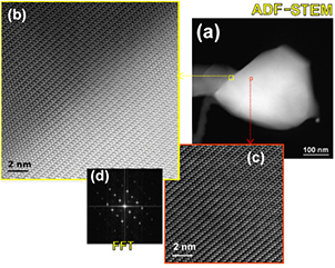
Figure 7. (a) ADF-STEM image of a selected nanowire tip, (b) atomic structure ADF-STEM image of the area framed in yellow in (a), and (c) atomic structure ADF-STEM image of the orange framed area, revealing no change in the crystal structure between wire and particle. This is confirmed by (d), showing the fast Fourier transform (FFT) of (b) being taken in the interface region, with only the reflections of β-Ga2O3 in ![$[1\text{\bar{1}2}]$](https://content.cld.iop.org/journals/0022-3727/47/43/435101/revision1/d501383ieqn014.gif) orientation.
orientation.
Download figure:
Standard image High-resolution imageWe thus suppose that the growth of the Fe-catalysed β-Ga2O3 NWs is mostly governed via a VLS mechanism. This requires the formation of an Fe–Ga–O alloy with the original Fe particle at the wire tip as verified by EDXS, and results in an increase in the volume of the particle.
3.2.3. XPS analysis.
Some additional information of composition on the surface of as-grown NWs has been obtained utilizing XPS measurements. Figure 8 shows a typical XPS survey spectrum of β-Ga2O3 NWs grown on sapphire at 950 °C for 3 h. The spectrum displays both the photoelectron and Auger electron peaks for Ga and O with carbon contamination. The peak position around 284.5 eV corresponds to the elemental carbon [41]. The binding energies around ~1118 and ~1145 eV are attributed to Ga 2p1/2 and Ga 2p3/2 electrons, respectively, as shown in figure 8(b). These sharp peaks around ~1118 and ~1145 eV for Ga 2p3/2 and Ga 2p1/2 core levels are associated with the Ga–O bonding in Ga2O3 [40, 41]. Figure 8(c) shows the O 1s peak around ~531 eV which is due to the presence of oxygen species in Ga2O3 [40–42]. From this XPS spectrum, the binding energy position of Ga 2p and O core levels are consistent with previous XPS studies [40–43]. This suggests that stoichiometric Ga2O3 NWs are synthesized properly on the sapphire substrate.
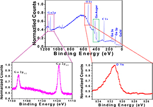
Figure 8. (a) X-ray photoelectron survey spectrum of Fe-catalysed β-Ga2O3 nanowires; (b), (c) core level spectra of Ga 2p and O 1s, respectively.
Download figure:
Standard image High-resolution image3.2.4. Raman analysis.
Figures 9(a) and (b) show typical micro-Raman spectra recorded at the centre of a single β-Ga2O3 NW and on a bulk Ga2O3 single crystal serving as reference. To the best of our knowledge, such a comparative Raman study is reported for the first time. We observed 11 clear Raman modes in the probed spectral range (124–800 cm−1) that are in excellent agreement with those published in the first, thorough Raman paper on this material [44]. Based on this similarity, we can unambiguously state that our β-Ga2O3 NWs have a monoclinic crystal structure and belong to the C2h group symmetry, implying a unit cell with two formula units, Ga2O6 octahedra and GaO4 tetrahedra. The measured Raman-active modes can be distinguished as follows: the first three peaks below 200 cm−1 correspond to the low-frequency libration and translation of tetrahedron–octahedron chains, the next four peaks between 300 and 500 cm−1 relate to the mid-frequency deformation of Ga2O6 octahedra, and the last four peaks between 600 and 800 cm−1 are attributed to the high-frequency stretching and bending of GaO4 tetrahedra [38, 44]. Table 1 summarizes the position of Raman peaks in the present study with respect to previous works [37, 38, 44] as well as the frequency shifts between the reference crystal and the NWs. Interestingly, we obtained quite small blue and red shifts ranging from 0.3 to 1.4 cm−1, in contrast to blue shifts of 10–40 cm−1 and red shifts of 4–23 cm−1 found with regard to pure Ga2O3 powder reference [37, 38]. These relatively small deviations indicate that the structural properties of our β-Ga2O3 NWs in terms of strain and defect levels are very close to those of a pure bulk Ga2O3 single crystal as shown in figures 9(a) and (b). The Raman results along with the other analyses demonstrate the growth of single crystalline β-Ga2O3 NWs using Fe as a new catalyst.
Table 1. Peak positions observed in the room temperature Raman spectra of a single β-Ga2O3 NW and a bulk Ga2O3 single crystal used as reference in comparison to previously published data.
| Dohy et al [44] | Rao et al [38] | Gao et al [37] | This work | ||||
|---|---|---|---|---|---|---|---|
| Frequency of bulk Ga2O3 (cm−1) | Frequency of bulk Ga2O3 (cm−1) | Frequency of bulk Ga2O3 (cm−1) | Frequency of powder Ga2O3 (cm−1) | Frequency of Ga2O3 nanorods (cm−1) | Frequency of Ga2O3 single crystal (cm−1) | Frequency of Fe–Ga2O3 NW (cm−1) | Frequency shifts Δω (cm−1) |
| 111.0 | |||||||
| 147.0 | 144.0 | 144.0 | 142.0 | 134.0 | 144.0 | 143.4 | −0.6 |
| 169.0 | 169.0 | 169.0 | 167.0 | 160.0 | 169.0 | 168.4 | −0.6 |
| 199.0 | 200.0 | 200.0 | 198.0 | 194.0 | 199.5 | 199.0 | −0.5 |
| 318.0 | 317.0 | 317.0 | 320.0 | — | 319.0 | 319.3 | +0.3 |
| 346.0 | 344.0 | 344.0 | 344.0 | 332.0 | 346.1 | 345.6 | −0.5 |
| 415.0 | 416.0 | 416.0 | 415.0 | 409.0 | 415.9 | 415.4 | −0.5 |
| 475.0 | 472.0 | 472.0 | 473.0 | — | 475.7 | 474.3 | −1.4 |
| 628.0 | 629.0 | 629.0 | 627.0 | — | 629.5 | 628.7 | −0.8 |
| 651.0 | 654.0 | 654.0 | 651.0 | 641.0 | 651.7 | 651.2 | −0.5 |
| 657.0 | 767.0 | 767.0 | 765.0 | 742.0 | 657.8 | 657.0 | −0.8 |
| 763.0 | 766.1 | 765.4 | −0.7 | ||||
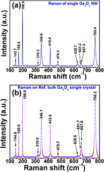
Figure 9. Typical Raman spectrum (a) recorded at the centre of a single β-Ga2O3 nanowire and (b) a reference single crystal of Ga2O3.
Download figure:
Standard image High-resolution image3.3. Optical properties
3.3.1. CL image analysis.
The SEM and its corresponding CL image are shown in figures 10(a) and (b). It is clear from the CL image that the luminescence originated from the entire length of NWs and NBs, indicating the existence of radiative centres. On the other hand, the entire region under these NWs and NBs appears black and behaves like a non-radiative centre. Recently, Navarro et al [45] studied the CL imaging and spectrum analysis of β-Ga2O3 NWs. They observed some bends, and it was suggested that these bends in the grown NWs were stacking faults which behaved as non-radiative centres. In addition, some triple junction nodes (called nanoflags) are observed along with β-Ga2O3 NWs and NBs, as shown with a red circle in figure 10(b). Johnson et al [23] have also observed some triangular shape type nanostructures in their controlled VLS growth of In2O3, Ga2O3, and SnO2 NWs via chemical vapour transport using Au catalyst. They suggested that these triangular shape nanostructures might be due to nucleation on twins or the presence of a small Au particle at the end of the NW.
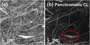
Figure 10. (a) 60° tilted-view SEM image and (b) corresponding panchromatic CL image of Fe-catalysed β-Ga2O3 nanowires taken for the UV–visible range.
Download figure:
Standard image High-resolution image3.3.2. CL analysis.
The RT-CL spectrum was measured for Fe-catalysed β-Ga2O3 NWs grown on sapphire in the UV–visible range (300–800 nm), as shown in figure 11. A very wide defect emission band, having a strong UV–blue and a weak red emission centred at ~398 nm (3.2 eV) and ~710 nm (1.75 eV), is observed in our CL spectrum, while no intrinsic emission (band to band emission) is visible in the above mentioned spectral range [17]. To have a better understanding of all defect emissions, the UV-CL spectrum was deconvoluted, and consists of mainly two Gaussian peaks at wavelengths (energies) positioned at 395 nm (3.13 eV) and 450 nm (2.76 eV). The first peak (3.13 eV) is related to UV emission, whereas the second (2.76 eV) peak is assigned to blue emission. The origin of all emission peaks is reported in many previous studies [46–52]. Harwig et al [49] suggested that the UV emission was attributed to recombination of self-trapped excitons. They proposed that this had an intrinsic nature and could not be changed with external factors such as temperature, growth time, pressure, and substrates. However, Villora et al [50] presented that UV emission (3.55 and 3.13 eV) is related to oxygen vacancies. The blue emission (~2.95 eV) is assigned to recombination of an electron on a donor and a hole on an acceptor or donor–acceptor pair (DAP). The donors are formed by oxygen vacancies (VO), whereas acceptors are formed by gallium (VGa) or gallium–oxygen vacancy pairs (VGa–VO) [48, 49]. The oxygen vacancies and gallium–oxygen vacancy pairs were produced at high growth temperature [46, 50, 51]. As we already mentioned that we have performed our experiment at a sufficient high temperature (950 °C). Thus, sufficient numbers of oxygen vacancies are present in as-grown NWs, which give UV as well as blue emission, in accordance with the study by Villora et al. In addition to UV–blue emission, we have also observed a weak red emission at 710 nm (1.75 eV) in our CL results. For the first time, Song et al [53] suggested that red emission was related to recombination of electrons trapped by oxygen vacancies and holes captured by deep level acceptor impurities such as nitrogen. In our previous study, we presented an energy band diagram of Ga2O3 revealing all emission bands. Furthermore, we compare CL spectra of as-grown β-Ga2O3 NWs with a bulk Ga2O3 single crystal, which consists of two bands. It is clearly visible that the two spectra are quite similar, and this might be caused by a higher degree of perfection of the structure of our as-grown NWs.
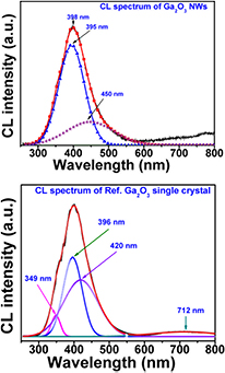
Figure 11. CL spectrum of Fe-catalysed β-Ga2O3 nanowires grown at 950 °C for 3 h on sapphire. The spectrum is deconvoluted with two Gaussian curves at wavelengths of 450 and 495 nm.
Download figure:
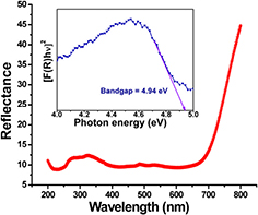
Standard image High-resolution image3.3.3. Bandgap analysis.
To estimate the bandgap of Fe-catalysed β-Ga2O3 NWs, the reflectance curve (figure 12) using a UV–visible–near infrared (UV–VIS–NIR) spectrophotometer is acquired. Then, we transformed this reflectance to the Kubelka–Munk (K–M) function F(R) using the K–M equation as described elsewhere [54]. The inset of figure 12 shows a plot of [F(R)hν]2 versus photon energy (hν) for β-Ga2O3 NWs on sapphire substrate. In the case of parabolic band structure, the bandgap Eg and absorption coefficient (α) of a semiconductor are related via the well known equation

where the value of m is 2 and 0.5 for indirect and direct bandgap semiconductors, respectively, and A is a constant. In the same way, the bandgap Eg and K–M function F(R) are also related by an equation as given in [54]

where B is another constant. The estimated bandgap from the experimental curve is ~4.94 eV for Fe-catalysed β-Ga2O3 NWs on sapphire substrate, which is in good agreement with the bandgap of β-Ga2O3 estimated in the previous studies [6, 32].
Figure 12. Bandgap calculation from K–M transformed reflectance spectrum of Fe-catalysed β-Ga2O3 nanowires grown at 950 °C for 3 h on sapphire.
Download figure:
Standard image High-resolution image
For comparison of NWs grown using different catalysts, we have published papers related to Au catalytic growth of β-Ga2O3 NWs [34, 35]. In the present study we have obtained single crystalline Fe-catalysed β-Ga2O3 NWs, which are comparable to the NWs grown using Au catalyst. CL properties are similar for the two catalysts. The bandgap of Fe-catalysed β-Ga2O3 NWs is 4.94 eV, whereas the Au-catalysed β-Ga2O3 NW bandgap was 4.74 eV [35].
4. Conclusions
In summary, we have successfully synthesized Fe-catalysed β-Ga2O3 NWs on sapphire substrate via the VLS growth mechanism. The XRD and Raman results revealed the crystalline nature of as-grown NWs. The as-grown NWs have diameters in a range of 30–80 nm, and lengths up to tens of micrometers. The electron microscope investigations by TEM, SAED and HR-ADF STEM demonstrated that β-Ga2O3 NWs were single crystalline, and grew preferentially along the normal of the  plane. As confirmed by STEM-EDXS, the NWs mainly consisted of Ga and O, whereas the nanoparticles at their tips additionally contained Fe. Raman spectra of β-Ga2O3 (being acquired from individual NWs) showed all three active frequency modes. In addition, a red shift of 0.3–1.4 cm−1 was observed when Raman spectra of as-grown β-Ga2O3 NWs and those of single crystals of Ga2O3 were compared. CL spectra obtained from the as-synthesized Fe-catalysed NWs and bulk Ga2O3 single crystal exhibited a strong UV–blue and a weak red emission. Furthermore, the bandgap of Fe-catalysed NWs was found to be around 4.94 eV. Hence, Fe is an alternative catalyst to grow single crystalline β-Ga2O3 NWs, and we plan to make NW based FETs using these NWs in future.
Acknowledgments
The authors gratefully thank the XRD and SEM measurement facilities of IIT Delhi. The authors SK and RS acknowledge the Nanoscale Research Facility (NRF) of IIT Delhi for providing partial financial support and the UV-visible measurement facility. One of the authors (SK) also acknowledges IIT Delhi for providing a research fellowship. The authors also thank Z Galazka, Institute for Crystal Growth (IKZ), Berlin, for providing bulk Ga2O3 single crystals for comparative studies. Funding received from the Nanomission program of Department of Science and Technology (DST), New Delhi, is gratefully acknowledged. The authors GS, CT and SC acknowledge the FP7 Projects Fiblys (grant 214042), Univsem (grant 280566) and LCAOS (258868) and the BMBF project Nawion (FKZ: 16SV5386K, V4MNI014) for partial financial support.