
Abstract
A plasmonic coupler, which consists of periodic metal gratings and a tapered waveguide, is integrated to a charge-sensitive infrared phototransistor (CSIP) for 45 µm wavelength radiation. The period and height of the gratings are about 42 µm and 4 µm, respectively. The gratings convert normally incident radiation into a surface wave, which is converged to the active region of the CSIP through the tapered waveguide. Both rise rate and signal amplitude become larger, due to the presence of the plasmonic coupler.
Export citation and abstract BibTeX RIS
1. Introduction
Detecting terahertz (THz) radiation has become increasingly important, in a wide range of fields including biology, imaging, securities and so on [1]. In particular, astronomical telescopes require sensitive detectors in the THz region, because a large proportion of radiation in the universe falls into this wavelength range [2–4]. THz photon counting has been demonstrated with an extraordinarily high sensitivity in quantum dot (QD) detectors, where a QD is photo-excited and sensed by a nearby single electron transistor [5–7]. Comparably good performance was later achieved in charge-sensitive infrared phototransistors (CSIPs), where an isolated region of two-dimensional electron gas (2DEG) is photo-excited due to intersubband transition (IST) and its excited charged state is sensed by a nearby 2DEG conducting channel [8–11]. CSIPs are easier to fabricate, and show promising features, such as a wide dynamic range (over 106), low output impedance (103–104 Ω) and relatively high operation temperatures (above 4.2 K). The CSIPs have so far been demonstrated for a set of far-infrared wavelengths (15–45 µm).
A CSIP is typically made of a bilayer 2DEG. It consists of a photo-sensitive floating gate (FG) and a source–drain conducting channel, as schematically illustrated in figure 1(a). The FG is an electrically isolated region in the upper quantum well (QW), defined by negatively biasing two metal front gates. The lower layer 2DEG works as the source–drain conducting channel. The electrons in the FG are photo-excited via IST in the QW similarly to the well-known quantum well infrared photodetectors (QWIPs) [12]. Unlike QWIP, the excited electrons escape to the lower layer 2DEG, as illustrated in figure 1(a). The FG is therefore positively charged, which affects the conductance of the source–drain channel in the lower layer 2DEG. The extremely large responsivity of the CSIP is due to the relatively long lifetime of the positive charge in the FG [8]. The quantum efficiency of the photoresponses is a product, e = ηCT, of the probability ηC that incident photons are absorbed via IST and the transmission probability T for the excited electrons to reach the lower layer 2DEG [9]. The photocoupler substantially affects ηC, while the crystal structure/quality determines T. In CSIP for 45 µm wavelength, the quantum efficiency was found to be distinctly smaller than that of the previously developed CSIPs for 14 µm [10, 11]. The sensitivity is accordingly smaller. This was interpreted as due to electron traps (Al–O complex) that cause multiple electron scattering within the interlayer region. Several proposals of suppressing Al–O concentration have been described [11].
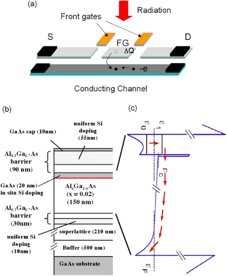
Figure 1. (a) Schematic representation of the CSIP. (b) Crystal structure and (c) energy diagram. In (b), a 2 nm-thick Al0.1Ga0.9As barrier layer (labelled using the thick red line) is just under the 20 nm-thick GaAs QW.
Download figure:
Standard image High-resolution imageEfforts can also be made to improve ηC, by increasing the field intensity at the FG. A strongly enhanced electric field has been realized in plasmonic structures, such as a single aperture surrounded by concentric gratings (sometimes known as the bull's eye structure) [13]. The enhancement of electric field has been ascribed to excitation of surface plasmon polaritons (SPP) [14], and has been observed over a wide range of electromagnetic wave spectra, from visible to microwave [15–17]. The scattering of light by the metallic gratings allows incident photons to be momentum matched to and coupled to surface plasmons [18, 19]. Focusing of SPP has been demonstrated with a laterally tapered plasmonic waveguide [20]. Designing more effective plasmonic couplers is becoming a promising approach for improving photodetector performance [21, 22].
Fabrication of plasmonic couplers for THz wavelength often involved creating micrometre-scale metal gratings, which was previously realized by cutting surface corrugation on a resin material and a coating of a gold layer [17, 21]. The finished coupler, however, has to be aligned on top of the photodetector, with, e.g., an x–y stage. Recently, projection-type photolithography and electroplating techniques have been applied to fabricate the bull's eye coupler, and to integrate the coupler to a THz photodetector. Markedly enhanced signals were observed [22]. In this paper, by applying the same techniques, we report a recent work for integrating plasmonic couplers to a CSIP, for λ = 45 µm radiation.
2. Experiment
The CSIP was fabricated from a modulation doped GaAs/AlGaAs heterostructure grown by molecular beam epitaxy on a semi-insulating GaAs substrate. As shown in figure 1(b), starting from the substrate, the crystal consists of a 500 nm-thick GaAs buffer, 210 nm-thick AlGaAs/GaAs superlattices (Al0.3Ga0.7As: 20 nm, GaAs: 1 nm, number repeated: ×10), a 30 nm Al0.3Ga0.7As barrier layer, a 150 nm-thick AlxGa1−xAs layer (x = 0.02), a 2 nm-thick Al0.1Ga0.9As barrier layer, a 20 nm GaAs upper QW layer, a 90 nm Al0.3Ga0.7As barrier layer and a 10 nm GaAs cap layer. The lower layer 2DEG is formed at the hetero-interface between the 150 nm-thick AlxGa1−xAs (x = 0.02) layer and the Al0.3Ga0.7As barrier layer, with electrons supplied by a 10 nm-thick uniformly doped layer (Si: 1 × 1018 cm−3) 20 nm below the interface. The upper layer 2DEG stays in the 20 nm-thick upper GaAs QW which is in situ doped with Si (2.5 × 1017 cm−3). And there is a 55 nm-thick uniformly doped layer (Si: 1 × 1018 cm−3) 35 nm above the upper QW. At T = 4.2 K, the as-cooled carrier density and mobility are 3.8 × 1011 cm−2 and 9 × 103 cm2 V−1 s−1 for the upper layer, and 1.1 × 1011 cm−2 and 1.4 × 104 cm2 V−1 s−1 for the lower layer, respectively. Figure 1(c) shows the energy diagram, which was derived via a self-consistent treatment of the Poisson and Schrödinger equations (nextnano3) [23].
Experimental results from two samples, A and B, are presented in this paper. Both samples have nearly identical CSIP, but with different coupler designs. Both samples have a semi-circular coupler. The coupler of sample B is plasmonic, with surface gratings, as shown in figure 2. The choice of the grating period was based on the following considerations. At THz frequency, in order for normally incident radiation to excite the SPP, the grating period (L) should be close to the target wavelength (λ) [19], which is the target wavelength of the CSIP. According to previous studies of similar structures, resonant excitation of the SPP occurs for L slightly smaller than λ, by 3–5% [17, 21]. This is likely due to mixing of direct grating scattering modes and cavity modes (in the cavity formed between adjacent gratings) [24]. The width and height of the gratings were optimized to be L/2 and L/10, respectively [17, 21]. A Bragg reflector (with a grating period of L/2) was included to suppress the energy propagating outwards, and to build up a stronger SPP [17]. The tapered waveguide focuses the SPP to further enhance the electric field at the tapered end, where the FG of the CSIP is located. Unlike sample B, the coupler of sample A does not have gratings, and was prepared for comparison purposes. The coupler of sample A is not expected to convert radiation to an SPP.
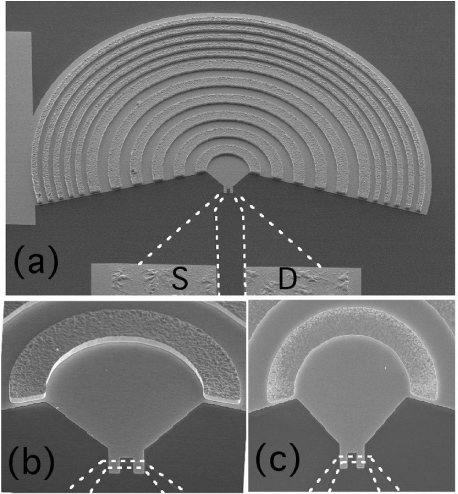
Figure 2. (a) Global view and (b), (c) centre region of sample B. The dashed lines indicate the edges of the mesa. 'S' and 'D' indicate the source and drain of the phototransistor.
Download figure:
Standard image High-resolution imageThe fabrication of the samples with plasmonic couplers includes two major steps. Before making the gratings, the CSIP is fabricated through standard photolithography, wet etching, metal film deposition and lift-off. Specifically, the 2DEG bilayers are formed into a 4 µm-wide constricted region by 80 nm-deep wet mesa etching. Ohmic contacts are formed by rapid annealing with 250 nm-thick AuGe/Ni to both layers. In the third step, electrical leads and the flat part of the couplers are deposited (15 nm Ti/250 nm Au). For sample B, the flat part is semi-circular, with a tapered extension. For sample A, the metal deposition is simply identical to that of sample B. The thickness of the gold layer (>250 nm) is much larger than the penetration length at THz frequency. The thick gold layer also guarantees smooth connection at the edge of the mesa.
For sample B, the gratings were made by electroplating thick gold on selective regions of the flat part (the deposited Au/Ti metal). To be specific, (1) 15 µm thick SU8-2010 photoresist was coated. (2) SU8 was exposed in a projection-type exposure system (DL1000, NanoSystem Solution Inc.), with a 405 nm laser at an energy density of 80 J cm−2. The pattern was focused at 8 µm below the upper surface of the resist. (3) After being developed in propylene glycol methyl ether acetate (PGMEA), slots with nearly vertical side wall were opened on the SU8 resist, where gold electroplating would create the gratings. (4) An AuI2-based electroplating solution, with brighteners and surfactants, was used [25, 26]. The electroplating was carried out at room temperature for about 30 min, with current density estimated to be 60 µA mm−2 and dc voltage at 150 mV. (5) In the final step, the SU8 resist was stripped off, by soaking the devices in hot remover PG (Microchem). As confirmed by a scanning electron microscope (SEM), the plated gold forms firm structures and a smooth surface, with grain size as small as 50 nm.
The measurement is made at 4.2 K. The sample is enclosed in a metal chamber submerged in liquid helium. A small window is left on the chamber, and is connected to a metal light pipe. A mechanical shutter is included. When the shutter is open, weak thermal radiation from upper warm parts of the metal light pipe is introduced into the sample, through the window. Visible light is blocked by black polyethylene filter. The intensity of relevant radiation (λ = 44 ± 1 µm) impinging on the photocoupler region of the devices is roughly estimated to be 400 pW4. The direction of the incident radiation is randomly distributed, as the light pipe is close to the perfect conductor for our interested wavelength. However, as will be discussed in the following paragraphs, the incident angle with respect to the sample surface may strongly affect the coupling between the radiation and the surface plasmon. To introduce a qualitative control, a short black polyethylene pipe is inserted into the lower end of the light pipe. Black polyethylene effectively absorbs radiations at 45 µm wavelength, with an absorption coefficient α = 50 cm−1 [27]. With the 0.6 mm thick pipe, an oblique ray would be markedly attenuated if it hits the side wall, even only once. The length-to-diameter ratio is 10. Therefore, the angle of incidence is estimated to be less than 1/10 rad.
3. Results
In figure 3(a), the dashed and solid lines show the source–drain conductance G, as a function of the gate bias voltage Vg, applied simultaneously to both front gates, for samples A and B, respectively. Data were taken at the source–drain bias VSD = 10 mV, under the dark condition. The step-like behaviour seen in the G versus Vg curve suggests the presence of the bilayer 2DEG, and that the upper QW is depleted in the gated region, for Vg below a threshold at Vg1 = −0.62 V. The inset shows G versus Vg of sample A under the dark and IR (infrared radiation) conditions. G becomes larger, in a range of Vg < Vg1 = −0.62 V, when the radiation is introduced into the sample. This change in G is the photosignal. The wavelength dependence of the photosignal was measured using a spectrometer consisting of a globar lamp, a conventional grating monochromator and a chopper. The external monochromatic radiation was chopped at f = 7 Hz. The signal was measured by a lock-in amplifier. As shown in figure 3(b), the resonant absorption occurs at about 44–45 µm, which is consistent with the theoretical calculation of intersubband energy spacing [23].
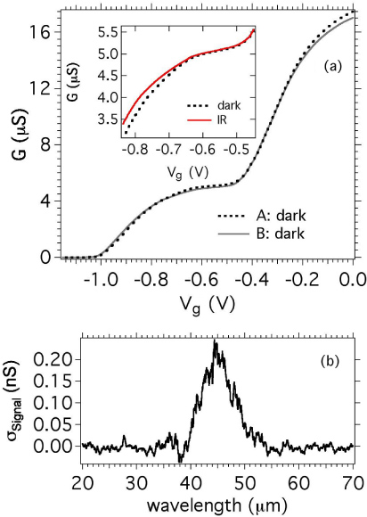
Figure 3. (a) The source–drain conductance G versus the gate bias voltage applied to both front gates, taken under the dark condition (sample A: dashed line, sample B: solid line). The inset shows the results for sample A, under the dark and IR (infrared radiation) conditions. (b) Dependence of photosignal on the wavelength of the incident radiation, taken for sample A.
Download figure:
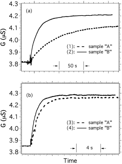
Standard image High-resolution imageFigure 4 shows the photoresponses for sample A (without gratings) and sample B (with gratings of 42 µm period, and a Bragg reflector), taken at Vg = −0.78 V. When the radiation is introduced into the sample by opening the shutter, G increases until it is eventually saturated. Figure 4(a) shows the case where the black polyethylene tube was inserted to the lower end of the light pipe, so that the radiation was expected to be roughly perpendicular to the sample surface. The rise of signal for sample B was five times quicker compared with that for sample A. The amplitude of the signal was 50% larger for sample B. Figure 4(b) shows the case where the black polyethylene tube was removed, so that oblique ray could also reach the sample. Compared with the case of normal incidence, the overall photoresponse was significantly quicker, for both samples. However, the difference between these two samples becomes smaller: the rise rate for sample B is only larger by 70%, compared with that of sample A. The signal amplitudes of the two samples are nearly identical.
Figure 4. Photoresponse ΔG versus time, for two samples (A and B), taken at T = 4.2 K. (a) The oblique radiation is expected to be absorbed by a black polyethylene tube at the lower end of the light pipe. (b) Both normal and oblique radiation could reach the sample. The CISPs of both samples are nearly identical. For sample A, the coupler does not have gratings. For sample B, the coupler has gratings of 42 µm period, and a Bragg reflector.
Download figure:
Standard image High-resolution image
4. Discussion
The effects of the plasmonic coupler show clear dependence on the direction of the incident radiation. In this experiment, the photosignal rise rate is predominantly determined by the occurrence of the IST. To excite the IST, only the electric field component perpendicular to the QW (or perpendicular to the sample surface) is relevant. Effects that could produce such a perpendicular component are divided into two major groups. (1) Plasmonic effects: the surface gratings of the plasmonic coupler convert the incident radiation into the SPP. The SPP gradually focuses as it propagates along the tapered waveguide, re-emits when it reaches the geometry termination of the metal, where the FG is located. (2) Non-plasmonic effects, which are those not related to the excitation of the SPP. For example, the front gates, with dimension substantially smaller than the target wavelength, scatter the incident radiation into the electric field alternating perpendicular to the QW. The oblique radiation itself has an electric field component that is perpendicular to the QW, even without any photocoupler. Our results suggest that the plasmonic effects dominate for the case of normal incidence. When oblique radiation can also reach the sample, the plasmonic effects are relatively weakened, as the grating period is designed predominantly for the normal incidence.
As a more quantitative analysis, we compare samples A and B, under two radiation conditions. With the black polyethylene filter, only the radiation with an incident angle less than 0.1 rad reaches the sample. Without the black polyethylene filter, the incident angle of the radiation may be distributed over a much broader range. The contributions of the perpendicular electric field, due to the two groups of effects mentioned in the previous paragraph, are summarized in table 1. Because the coupler of sample A does not have surface gratings, I1A ≈ 0, J1A ≈ 0. It is reasonable to take I2A = I2B = I2 and J2A = J2B = J2. From the rise of the signals in figures 4(a) and (b), we get IB ≈ 6 × IA, JB ≈ 13 × IB, and JB ≈ 1.7 × JA. Although it is impossible to get all unknown variables, we can derive that J1B ≈ 6.4 × I1B, J2 ≈ 46 × I2. The result of J1B ≈ 6.4 × I1B is consistent with that the period of the surface gratings is well designed for normal incidence only. On the other hand, the non-plasmonic effects are, in total, much less sensitive to the incident angle, therefore become markedly stronger when the oblique radiation reaches the sample.
Table 1. Intensity of (EZ)2 averaged over the FG region for samples A and B, under two radiation conditions. EZ is electric field perpendicular to the QW. Two groups of effects are considered to contribute to EZ. Effects in group 1 are due to coupling of the radiation to the SPP. Group 2 includes those effects that are non-plasmonic, such as scattering of incident radiation by the sub-wavelength metal front gates, EZ component of the incident radiation.
| Radiation | Normal incidence (incident angle <0.1 rad) | Normal + oblique incidence (incident angle < π/2) | ||
|---|---|---|---|---|
| Samples | 'A' | 'B' | 'A' | 'B' |
| Group 1 | I1A ≈ 0 | I1B | J1A ≈ 0 | J1B |
| Group 2 | I2A | I2B | J2A | J2B |
| In total | IA = I1A + I2A | IB = I1B + I2B | JA = J1A + J2A | JB = J1B + J2B |
The amplitude of the photosignal is determined by the equivalence that the number of electrons escaping the FG equals the number of electrons coming back from the lower layer. The amplitude starts to become smaller, when the excitation is reduced below a threshold [10]. In our experiment, the saturated signal amplitude remains nearly unchanged over a wide range of excitation levels (conditions 2–4, in figures 4(a) and (b)), but is markedly smaller when the excitation is sufficiently weak (condition 1, in figure 4(a)). Our experimental results are qualitatively consistent with the theoretical picture and the earlier studies [10].
Although the main purpose of this paper is to demonstrate the effects of surface gratings, we briefly estimate the key parameters of the detector. The conductance (G1) of the constricted region of the lower conducting channel (immediately below the FG) increases by ΔG1 ≈ (W/L)Δneμ = ΔQμ/L2, if charge ΔQ is photo-induced on the FG. This is because the electron density in the constricted region under the FG increases by Δn = ΔQ/(WLe). Here μ is the electron mobility of the lower layer 2DES, and W and L are the width and length of the FG, respectively. The total source–drain conductance increases by ΔG = (G2/(G1 + G2))2 × ΔG1, where G2 is the conductance of the lead regions connecting to the source and drain contacts. For the geometry shown in figure 2, ΔG = 0.013 × ΔG1. Noting μ = 2.4 × 104 cm2 V−1 s−1, L = 8 µm, we estimate ΔG+e = 0.078 nS, for the event of single electron escape ΔQ = +e. This implies that the photosignal is saturated when ΔQsat ≈ +5100e is reached. As shown in figure 4(b), the rise time is taken to be 1 s, within which the number of photons hitting the coupler is estimated to be 1 × 10¹¹. The quantum efficiency is therefore ∼5 × 10⁻⁸. The noise equivalent power of the detector,
 , is estimated to be 8 × 10⁻¹³ W Hz−1/2, by noting the signal-to-noise ratio (SNR) ∼ 500 from the data in figure 4, averaging time of the measurement ∼1 s, and the radiation power P ∼ 400 pW falling on the coupler area. We emphasize that the poor parameters of the detector are partly due to the large area of the coupler. However, the coupler is important, as long as it helps in enhancing the electric field intensity in the active region (the FG for CSIPs).
5. Summary
To conclude, plasmonic couplers were integrated onto a CSIP for 45 µm wavelength radiation. For normally incident illumination, the rise time of the photosignal was reduced by a factor of 6, and the amplitude of the signal was enhanced. In recent years, there has been considerable interest in the field of plasmonics. The integration of photodetectors and plasmonic couplers also helps us to offer a test ground for a variety of plasmonic structures.
Acknowledgments
This work was supported by the foreign postdoctoral researcher (FPR) program of Riken.
Footnotes
- 4
400 pW is roughly estimated, based on the photoresponses of a standard CSIP, under similar measurement conditions. The standard CSIP was carefully calibrated in 'an all cryogenic spectrometer [8]', where well-defined radiation from a black body emitter was used to determine its absolute sensitivity.