
Abstract
We present an infrared perfect absorber model composed of gold nanobars and a photonic microcavity. The inevitable losses in metamaterials are taken as an advantage for high absorbance efficiency. By adjusting the structural geometry, the device can be used for refractive index sensing. In our calculation with a spacer thickness H = 90 nm it can yield more than 99% absorbance in the near-infrared frequency region. The full-width at half-maximum can be realized up to an extremely narrow value of 40.8 nm and the figure of merit can be obtained as high as 357. For sensing applications with a perfect absorber, our work can serve as a model of coupling between the localized surface plasmon within nanoparticles and the propagating surface plasmon along the planar metal layer. The novel concept has great potential to maintain its performance of localized surface plasmon in practical applications.
Export citation and abstract BibTeX RIS
1. Introduction
Localized surface plasmon resonance (LSPR) is attributed to the strong interaction between the conduction electrons and incident electromagnetic field within a subwavelength metallic nanostructure [1]. Contrary to the LSPR, when the interface of the metallic structure is large enough, the plasmon can propagate in the form of an oscillating charge wave, which is referred to as the propagating surface plasmon (PSP) [2]. The two plasmonic properties have been considered as the foundation of many fascinating applications in biosensing [3–5], surface-enhanced Raman spectroscopy (SERS) [6, 7] and second harmonic (SH) generation [8]. In combination with a thin metal layer, the subwavelength structure confines the electromagnetic energy and allows the hybridization of localized plasmon modes with the resonator modes in the microcavity between them [9–13].
The LSPR strongly depends on the shape, composition, size, light polarization and surrounding dielectric environment of the subwavelength metallic nanostructures. Particularly, the latter dependence opens a way towards refractive index sensing, which can be used to detect small quantities preferably down to single molecules. Recently, different plasmonic structures, such as nanoshells, nanospheres and so on, have been proposed to detect the large spectral shift for the changes in refractive index [14–17]. Moreover, some special physical mechanisms, such as the tunability of subradiant dipolar and Fano-type plasmon resonances, the symmetry breaking in plasmonic nanocavities, and especially the classical analogue of electromagnetically induced transparency, are explored for more sensitive and prospective sensors [18–21]. No matter what the new configurations or mechanisms, the inevitable losses constrain the development of those sensors in practical applications. Nevertheless, a creative idea based on metamaterials turns the losses to be advantageous by introducing the concept of a perfect absorber. Metamaterials are subwavelength metallic nanostructures with unit cells much smaller than the operating wavelength of incident light [22–24]. The basic principle of a perfect metamaterial absorber is to minimize the reflectance through impedance matching or some other methods, and to simultaneously eliminate the transmittance by maximizing the metamaterial losses [10]. Alternatively, perfect absorption can also be achieved with microcavity, holes arrays and metallic surfaces.
For plasmonic sensors, the sensitivity (S) is commonly defined in terms of the change or shift of a measurable parameter, typically the resonant wavelength, for detection of refractive index. The full-width at half-maximum (FWHM) is another factor determining the performance of plasmonic sensors. It is strongly dependent on the shape and size of the nanoparticles. Some results have indicated that linewidth narrowing is potentially helpful in improving the performance of LSPR sensors [13]. Generally, an overall performance parameter of the plasmonic sensor is defined as the figure of merit (FOM), FOM = S/FWHM. This definition allows nanoparticles to be judged against one another as sensing platforms independent of shape and size [25]. However, this overall performance suffers from the restriction of Lorentz resonance peak shape, as well as the measuring device, such as the spectrometer. As an alternative, FOM*, defined as FOM* = [(dI/dn)/I]max, can be used to evaluate the performance of the plasmonic sensor since the intensity change dI is much easier to detect in an experiment using, for example, a laser diode, at a fixed wavelength λ0 induced by a refractive index change dn rather than that of the wavelength [26]. And it is appropriate to those resonant peaks which do not follow the Lorentz shape. Recently, considerable attention has been paid to the improvement of FWHM or FOM* by optimizing the structure dimensions or adopting new mechanisms [26, 27]. However, most of the studies just concentrate on only a single parameter, such as FWHM or FOM*, and ignore the other parameters. It is well known that a new structure with simple configuration and good performance, particularly narrower FWHM and higher FOM*, is still expected.
In this paper, we present a novel plasmonic sensor with the introduction of an infrared perfect absorber. The device can yield more than 99% absorbance in the calculated results. Our work has indicated that the FWHM is as narrow as 40.8 nm and the FOM* is as high as 357. We also show that the spacer thickness between the nanobars and the planar metal layer is of particular importance to the performance of absorbance efficiency, and consequently plays a key role in sensing qualities. The mechanism of LSP and PSP interaction is proposed to explain the effect of spacer thickness on the absorbance efficiency.
2. Structures and the simulation method
Figure 1 illustrates the schematic geometry of the infrared perfect absorber. It consists of three layers over the quartz substrate. The bottom is a large gold planar mirror and the top an array of periodic gold nanobars. The unit cell of the nanobars is composed of two bars with the same parameters. The spacer between the two layers, namely the microcavity, is filled with SiO2. The test liquids or gases are channelled or diffused over the periodic gold nanobars. The structure has dimensional parameters as follows: bar length (L), width (W), thickness (T) and gap distance (D), the lattice constant in the x-axis (P1) and in the y-axis (P2), the dielectric spacer thickness (H) and the planar gold layer thickness (G). To investigate the resonant behaviour of the absorber, we employ the commercial software EastFDTD (from Dongjun Information Technology Co., Ltd), which is based on the 3D finite-difference time-domain method, for calculation. For the excitation of the structure, a normal incident light with its polarization along the x-axis is adopted. The refractive index of the dielectric spacer in the NIR region is taken as 1.4. The permittivity of bulk gold in the frequency range is described by the Lorentz–Drude model [28]. In our calculation, the damping constant of the gold film is set to be higher than that of bulk gold owing to the grain boundary effects and the surface scattering in real thin films [29]. With an adjustment of the spacer thickness, the inevitable losses, which a traditional study would want to avoid, are desirable in our results.

Figure 1. Schematic of the sensing structure and the coordinate setup configuration. The whole structure is placed on the quartz substrate.
Download figure:
Standard imageFor the existence of bottom layer, the transmittance of the absorber is almost totally eliminated in the near-infrared (NIR) region, as shown in figure 2. The transmission value is so small not only at the resonant wavelength but also in the near-infrared regime that it can be looked as T = 0. In this way the absorbance can be calculated by 1 − R (R is the resonant reflectance dip intensity). The perfect absorber can be achieved just by minimizing the reflectance dip intensity and fortunately it can be easily realized by adopting different nanoparticle shapes, changing the lattice constant or rationally designing the other structure dimensions. Among these choices, optimizing the spacer thickness offers a simple and efficient method to reach nearly absolute absorbance. Here, special attention is paid to the optimization of dielectric spacer thickness for maximum absorbance. In such a situation, our results demonstrate the realization of the narrow FWHM and high FOM*.

Figure 2. Calculated reflection and transmission spectra for H = 90 nm with the other parameters given in section 3. The transmission values are all less than 0.001 in the NIR regime.
Download figure:
Standard image3. Results and discussion
To have a direct look at the effects of spacer thickness on the sensing qualities, we first show the reflection spectrum in figure 2 qualitatively. Then in figures 3 and 4, we quantitatively show the resonant dip position shift, the intensity change, and the FWHM and FOM*, respectively. The test liquid over the nanobars is a 25% solution of glucose in water with refractive index n = 1.3594 [30] for figures 2 and 3. For the determination of FOM*, a measurement with water n = 1.3198 [31] is performed in figure 4. The other parameters of the structure are preliminarily optimized and given as follows: L = 380 nm, W = 100 nm, T = 70 nm, D = 120 nm, P1 = 500 nm, P2 = 500 nm and G = 40 nm.
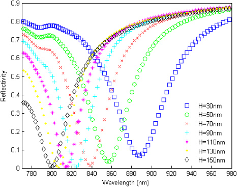
Figure 3. Simulated reflection spectrum of the sensing structure as a function of the dielectric spacer thickness from H = 30 nm to H = 150 nm for a 25% solution of glucose in water. Within the large thickness range the structure achieves high absorbance efficiency.
Download figure:
Standard image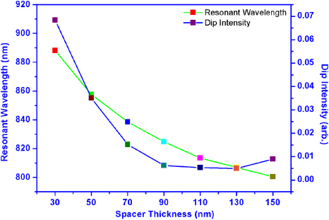
Figure 4. Calculated resonant wavelength and the dip intensity at different spacer thicknesses. The resonant wavelength has a blueshift but the dip intensity has changed by less than 0.07.
Download figure:
Standard imageAs shown in figure 2, there are a series of strong reflectance dips. Here we emphasize that the shape of the spectrum becomes more and more asymmetric as the spacer thickness increases. The intensity of the short wavelength part decreases to be less than half of that of the long wavelength part. Considering that the FWHM values are obtained from the Lorentz fitting of the plasmon resonant dips, the reflection spectra are not carried out with thicknesses more than 150 nm. Furthermore, it becomes symmetric again for thicknesses more than about 300 nm, but the FWHM is more than twice wider than that shown in figure 2. Based on the above discussions, we shall not take the thickness to be more than 150 nm.
To make a systematic discussion of the structure, we present the resonant wavelength, dip intensity, FWHM and FOM* quantitatively in figures 3 and 4. It can be seen that over a wide range of spacer thicknesses the resonant dip intensities are all below 0.1 and change by less than 0.07. However, the maximum of the absorbance can reach more than 99.5% for H = 110 nm. As shown in figure 3, the absorbance has a very small change and shows low sensitivity to the thickness. Depending on the low thickness sensitivity of absorbance efficiency, this structure offers more choices of thickness and we can pay more attention to the FWHM and FOM*. Moreover, we can see that the resonant wavelength has a blueshift. The resonant wavelength is located at 888.1 nm for H = 30 nm and undergoes a blueshift to 800.5 nm when the thickness increases to 150 nm. The blueshift of the resonant wavelength is attributed mainly to the plasmonic coupling between LSP of the nanobars and PSP of the bottom gold layer. The dipole resonance in the bars results in the creation of image charges in the bottom layer, effectively leading to a quadrupole resonance. In figure 6 we discuss these interactions in detail.
Figure 5 quantitatively shows the FWHM and FOM* as a function of the spacer thickness and elsewhere in the text. The two parameters are highly sensitive to the thickness. It can be seen that the FWHM is 60.4 nm at H = 30 nm and has a big decrease up to H = 70 nm. Then the FWHM remains nearly constant at a value of 40 nm from H = 70 to 110 nm. After the stable step, it goes through a fast increase up to 60.7 nm from H = 110 to 150 nm. Notably, the FOM* has a nearly opposite trend relative to the FWHM. From H = 30 to 150 nm, the FOM* increases first, then approaches a value of 357 at H = 90 nm, and finally has a sharp fall up to H = 150 nm. The variation range is more than 300. From figure 5 we can see that the FWHM and FOM* obviously depend on the spacer thickness. Fortunately, we get the optimization results of FWHM = 40.8 nm and FOM* = 357 at H = 90 nm and the values satisfy the requirement of narrow FWHM and high FOM* in the applications of plasmonic resonance sensing.

Figure 5. Calculated FWHM and FOM* at different spacer thicknesses. The FWHM remains nearly unchanged around 40 nm from H = 70 nm to H = 110 nm while the FOM* has a peak of 357 at H = 90 nm.
Download figure:
Standard imageTo have a better look at the characteristic of the perfect absorber, the distribution of magnetic field at resonant frequency is depicted in figure 6. The circling field in the nanobars is perpendicular to the electric field. According to the Maxwell equation, it is known that the surface currents are excited antiparallel in the nanobars and bottom mirror, respectively. Generally, the circulating current is considered to be a magnetic moment and it has a strong coupling with the incident magnetic component of the electromagnetic wave. Moreover, the accumulation of opposite charges at both ends of the bars forms an electric moment which has an interaction with the incident electric field. Thus, the electromagnetic energy is mostly confined in the small volume of the dielectric spacer. Here, we know that the nanobar dimensions are much smaller than the resonant wavelength, so the simple quasi-static approximation is appropriate in such a situation. From another viewpoint, the energy confinement can be explained by the mode hybridizations between LSP in the nanobars and PSP along the bottom gold layer. The formed microcavity acts as a capacitor storing the energy and gives rise to the reflectance resonant dip with nearly absolute absorbance in the spectrum as depicted in figure 2.
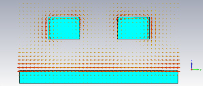
Figure 6. Simulated magnetic field distribution of the yz plane at resonant frequency, where the nearly absolute absorbance occurs.
Download figure:
Standard image4. Conclusions
In summary, we have presented a novel plasmonic sensor of perfect absorber in the near-infrared region. We take the advantage of the metamaterial inevitable losses to design the nanobar arrays near a gold film with an SiO2 spacer. It is numerically indicated that the spacer thickness is of great importance to the FWHM and the FOM*. The mechanism of LSPR and PSP interaction is proposed to explain the perfect absorbance and the energy confinement in the dielectric spacer. Finally, the expected narrow FWHM of 40.8 nm and high FOM* of 357 is achieved. Our work has great potential to serve as a practical plasmonic resonance sensor by taking advantage of losses with a perfect absorber.
Acknowledgments
This work was supported in part by the State Key Program for Basic Research of China Grant No 2007CB613206, the National Natural Science Foundation of China Grant Nos 10725418, 10734090, 10990104 and 60976092, the Fund of Shanghai Science and Technology Foundation Grant Nos 09DJ1400203, 09ZR1436100, 10JC1416100 and 10510704700.